Language selection

Search

Patent 1274887 Summary

Third-party information liability

Some of the information on this Web page has been provided by external sources. The Government of Canada is not responsible for the accuracy, reliability or currency of the information supplied by external sources. Users wishing to rely upon this information should consult directly with the source of the information. Content provided by external sources is not subject to official languages, privacy and accessibility requirements.

Claims and Abstract availability

Any discrepancies in the text and image of the Claims and Abstract are due to differing posting times. Text of the Claims and Abstract are posted:

  • At the time the application is open to public inspection;
  • At the time of issue of the patent (grant).
(12) Patent: (11) CA 1274887
(21) Application Number: 526819
(54) English Title: DAUGHTER BOARD/BACKPLANE ASSEMBLY
(54) French Title: ENSEMBLE CARTE-FILLE/FOND DE PANIER
Status: Expired
Bibliographic Data
(52) Canadian Patent Classification (CPC):
  • 347/34
  • 339/7.1
(51) International Patent Classification (IPC):
  • H05K 7/14 (2006.01)
  • H05K 3/36 (2006.01)
(72) Inventors :
  • JOHNSON, LENNART BORGE (United States of America)
(73) Owners :
  • TERADYNE, INC. (United States of America)
(71) Applicants :
(74) Agent: SMART & BIGGAR
(74) Associate agent:
(45) Issued: 1990-10-02
(22) Filed Date: 1987-01-07
Availability of licence: N/A
(25) Language of filing: English

Patent Cooperation Treaty (PCT): No

(30) Application Priority Data:
Application No. Country/Territory Date
817,013 United States of America 1986-01-08

Abstracts

English Abstract


Abstract of the Disclosure
A daughter board/backplane assembly including a
backplane having first and second surfaces and holes
extending from the first surface to the second surface,
pairs of separate first contacts having first ends
mounted in the holes and second ends extending from both
ends of the holes, the second ends of each first contact
being positioned with respect to he respective surface
from which it extends, and a plurality of daughter
boards mounted on opposite sides of the backplane and
carrying second contacts mating with the second ends of
the first contacts.


Claims

Note: Claims are shown in the official language in which they were submitted.


- 5 -

THE EMBODIMENTS OF THE INVENTION IN WHICH AN EXCLUSIVE
PROPERTY OR PRIVILEGE IS CLAIMED ARE DEFINED AS FOLLOWS:
1. A daughter board/backplane assembly
comprising
a backplane having first and second surfaces
and holes extending from said first surface to said
second surface,
pairs of separate first contacts having first
ends mounted in said holes and second ends extending
from opposites ends of said holes, each said second end
being positioned with respect to the respective surface
from which it extends, and
a plurality of daughter boards mounted on
opposite sides of said backplane and carrying second
contacts mating with said second ends of said first
contacts extending from both said first and second
surfaces.

2. The assembly of claim 1 wherein said holes
through said backplane are plated-through holes.

3. The assembly of claim 2 wherein said first
ends of said first contacts are expanded hollow portions
that are press fit into said holes.

4. The assembly of claim 3 wherein there is a
shoulder between said first end and said second end of
each said first contact.

5. The assembly of claim 1 further comprising
a backplane connector element that is made of insulating
material, engages a plurality of said first contacts and
has sidewalls extending generally parallel to said first
contacts, and said daughter boards have daughter board
connector elements designed to mate with said sidewalls
of said backplane connector element.

- 6 -

6. The assembly of claim 5 wherein said first
contacts have second ends that are pins, and said second
contacts are forks designed to mate with said pins.

7. The assembly of claim 4 further comprising
a backplane connector element that is made of insulating
material, engages a plurality of first contacts, and has
sidewalls extending generally parallel to said first
contacts, and wherein said shoulders touch a lower
surface of said backplane connector element, and said
daughter boards have daughter board connector elements
designed to mate with said first sidewalls of said
backplane connector element.

Description

Note: Descriptions are shown in the official language in which they were submitted.


DAUGHTER BOARD/BACKPLANE ASSEM~LY

Field o-f the Invention
The invention relates -to daughter
board/backplane connection systems.

Background of _he Invention
A plurality of daughter boards are often
detachably mounted on one side of a backplane and
electrically connected to each other througll pin
contacts mounted in the backplane and electrically
connected to other pin contacts via conducti~e paths
incorporated in the backplane or wires or bus bars
connected between wire wrap portions of the pin contacts
extending underneath the backplane.
As rise times for electronic signals between
components and data processing time continue to
decrease, the distance a signal has to travel from one
daughter board to another is becoming a more critical
consideration. Prior to the invention claimed herein,
someone who was not obligated to assign rights to the
assignee of this application suggested mounting daughter
boards on opposite sides of a backplane to provide
shorter paths between components on different boards.

Summary of the Invention
I have discovered that in providing a
connection system for daughter boards mounted on both
sides of a backplane, I could advantageously use pairs
of separate contacts mounted in common holes through the
backplane so that the portions of the contacts extending -
from the opposite sides of the backplane could be
accurately and independently positioned with reference
to the surfaces from which they extend regardless of the

.
~ih r

~7~7

-- 2

backplane thickness and still provide good high-speed
electrical transmission.
In preferred embodiments the contacts extending
from the backplane are pin contacts having expanded
portions that are press fit into plated-through holes in
the backplane; the pin contacts have shoulders between
the expanded portions and the ends extending from the
backplane; and a plastic backplane connector element
supports a plurality of rows of the pin contacts and has
upstanding sidewalls for engaging a mating daughter
board connecting element with a corresponding plurality
of mating contacts.
Other advantages and features of the invention
will be apparent from the following description of a
preferred embodiment thereof and from the claims.

Description of the Preferred Embodiment
Drawing
The drawing is a diagrammatic vertical
sectional view showing a daughter board/backplane
assembly, partially disconnected, according to the
invention.
Structure
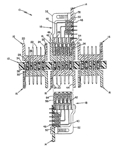
Referring to the drawing, there is shown
daughter board/backplane assembly 10 including backplane
12 and daughter boards 14 electrically connected to each
other through backplane connector elements 16 and
daughter board connector elements 18. Backplane
connector elements 16 include plastic housing 20 and
four rows of pin contacts 22 mounted in the base of
housing 20 and extending away from the backplane.
Backplane connector element 16 also includes fifth row
contact5 24, which are carried by sidewall 26 and are
used for ground or voltage. Each pin contact 22 has a


lower end with eY~panded portion 28 that is press Eit
into a plated-through hole 30 of baclcplane 12. The
length of each expanded portion 28 is less than one-half
of the thickness of backplane 12, to permit a pair of
pin contacts 22 to share a common hole 30. Pin contacts
22 have shoulders 32, to accurately position pin
contacts 22 with respect to housings 20 and either upper
surface 34 or lower surface 36 of backplane 12.
Daughter board connector element 18 includes
contacts 40 that are forked at ends 42 in boxes 44 of
plastic housing 46 and are bent horizontally at the
other ends 48, which pass through plastic guide board 50
and holes in daughter board 14, where they are
soldered. Aluminum stiffener 52 is connected between
guide board 50 and housing 46 to cover exposed portions
of contacts 40 and provide structure to daughter board
connector element 18. On the outer face of sidewall 54
of housing 46 are fifth row ground contacts 56, mating
with fifth row contacts 24 of the backplane connector
element.
In manufacture, pin contacts 22 are first
inserted into plastic housing 20 until shoulders 32
contact the lower surface of housing 20. A loading head
is placed over the pointed ends of pin contacts 22, and
the expanded portions 28 are pushed into holes 30, the
loading head pushing against the tips of pin contacts 22
and against shoulders 32 (through housing 20) until the
lower surface of housing 20 touches upper surface 34 or
lower surface 36 of backplane 12. The expanded portions
of contacts 24, not seen in the figure owing to their
orientation, are similarly press-fit into respective
plated-through holes.
In making connection through the backplane, the
goal of minimizing the number of connections in order -to

improve electrical transmission would indicate using a
single pin passing through each hole, particularly in
light of the desire to reduce distortions caused at
connection points in the increasingly hiyher speed
designs; accurate location of both ends of single pins
would be difficult, and would require precise backplane
thickness. By using two pin contacts 22 in the same
hole, they are independently precisely located with
respect to upper surface 34 and lower surface 36,
regardless of the thickness of backplane 12, the
tolerance for which might be as much as 0.030" with a
0.180" thick backplane, and good high speed electrical
transmission is still provided.
Operation
Operation of daughter board/backplane assembly
10 is as usual, daughter board connector elements 1~
being inserted into backplane connector elements 16 to
electrically connect daughter boards 14.

Other Embodiments
Other embodiments of the invention are within
the scope of the following claims.


.. . . .

Representative Drawing
A single figure which represents the drawing illustrating the invention.
Administrative Status

For a clearer understanding of the status of the application/patent presented on this page, the site Disclaimer , as well as the definitions for Patent , Administrative Status , Maintenance Fee  and Payment History  should be consulted.

Administrative Status

Title Date
Forecasted Issue Date 1990-10-02
(22) Filed 1987-01-07
(45) Issued 1990-10-02
Expired 2007-10-02

Abandonment History

There is no abandonment history.

Payment History

Fee Type Anniversary Year Due Date Amount Paid Paid Date
Application Fee $0.00 1987-01-07
Registration of a document - section 124 $0.00 1987-03-17
Maintenance Fee - Patent - Old Act 2 1992-10-02 $100.00 1992-09-01
Maintenance Fee - Patent - Old Act 3 1993-10-04 $100.00 1993-09-14
Maintenance Fee - Patent - Old Act 4 1994-10-03 $100.00 1994-09-14
Maintenance Fee - Patent - Old Act 5 1995-10-02 $150.00 1995-09-14
Maintenance Fee - Patent - Old Act 6 1996-10-02 $150.00 1996-09-16
Maintenance Fee - Patent - Old Act 7 1997-10-02 $150.00 1997-09-10
Maintenance Fee - Patent - Old Act 8 1998-10-02 $150.00 1998-09-10
Maintenance Fee - Patent - Old Act 9 1999-10-04 $150.00 1999-09-20
Maintenance Fee - Patent - Old Act 10 2000-10-02 $200.00 2000-09-21
Maintenance Fee - Patent - Old Act 11 2001-10-02 $200.00 2001-09-21
Maintenance Fee - Patent - Old Act 12 2002-10-02 $200.00 2002-09-19
Maintenance Fee - Patent - Old Act 13 2003-10-02 $200.00 2003-09-22
Maintenance Fee - Patent - Old Act 14 2004-10-04 $250.00 2004-09-21
Maintenance Fee - Patent - Old Act 15 2005-10-03 $450.00 2005-09-21
Maintenance Fee - Patent - Old Act 16 2006-10-02 $450.00 2006-09-29
Owners on Record

Note: Records showing the ownership history in alphabetical order.

Current Owners on Record
TERADYNE, INC.
Past Owners on Record
JOHNSON, LENNART BORGE
Past Owners that do not appear in the "Owners on Record" listing will appear in other documentation within the application.
Documents

To view selected files, please enter reCAPTCHA code :


To view images, click a link in the Document Description column. To download the documents, select one or more checkboxes in the first column and then click the "Download Selected in PDF format (Zip Archive)" or the "Download Selected as Single PDF" button.

List of published and non-published patent-specific documents on the CPD .

If you have any difficulty accessing content, you can call the Client Service Centre at 1-866-997-1936 or send them an e-mail at CIPO Client Service Centre.


Document
Description 
Date
(yyyy-mm-dd) 
Number of pages   Size of Image (KB) 
Representative Drawing 2001-09-20 1 20
Description 1993-10-13 4 143
Drawings 1993-10-13 1 49
Claims 1993-10-13 2 55
Abstract 1993-10-13 1 17
Cover Page 1993-10-13 1 15
Fees 1992-09-01 1 29
Fees 1993-09-14 1 28
Fees 1994-09-14 1 41
Fees 1995-09-14 1 30
Fees 1996-09-16 1 30
Fees 2006-09-29 1 35