Note: Descriptions are shown in the official language in which they were submitted.
The present invention relates to an image sensing
apparatus using a photoelectric conversion element having a
photoelectric charge storage region in which a potential is
controlled by a capacitor.
An image sensing apparatus according to the present
invention is applicable to image input devices, workstations,
digital copying machines, wordprocessors, bar code readers,
and automatic focusing photoelectri~ conversion object
detection devices for cameras, video cameras, 8-mm movie
cameras, and the like.
~ esearch on photoelectric conversion devices and in
particular on solid state sensors is concentrated on CCD and
MOS devices.
In a CCD sensor, a potential well is formed below a
MOS capacitor electrode. A charge generated upon reception
of light is stored in the well. During readout, the
potential wells are sequentially operated by pulses applied
to the electrodes, and the stored charges are transferred to
an output amplifier. The CCD sensor therefore has a
relatively simple structure, generates low noise, and allows
image sensing at low luminances.
The operation principle of a MOS sensor is as
follows. Upon reception of light, charges are stored in
photodiodes of p-n junctions constituting light-receiving
sections. During readout, MOS switching transistors
connected to the respective diodes are sequentially read out
~,~Jb
to an output amplifier. Ther~fore, a MOS sensor has a more
complex structure than a CCD sensor. However, a MOS sensor
can have a high storage capacity and wide d~lnamic ranye.
O~ the two types of conventional sensors described
above, a CCD sensor has the following drawbacks.
1) Since a MOS amplifier is formed on a chip as an output
amplifier, 1/f noise is generated from the interface between
the Si and the silicon oxide film, thus interfering with
normal display.
lo 2) When the number of cells is increased and cells are
integrated at a high speed in order to provide high
resolution, the maximum charge amount which can be stored in
a single potential well is reduced and a wide dynamic ran~e
cannot be obtained.
3) Since a CCD sensor has a structure wherein stored charges
are transferred, if even a single cell fails the transferred
charges stop at the failed cell. Thus manufacturing yield
is low.
An MOS sensor has the following drawbacks.
1) Since a wiring capacitance is connected to each
photodiode, a large signal voltage drop occurs when a signal
is read out.
2) Wiring capacitance is large, and random noise is easily
generated.
3) Fixed pattern noise tends to become mixed in due to
variations in the parasitic capacitance of a scanning MOS
switching transistor. Hence, image sensing at low luminances
cannot be performed. When cells are reduced in size in order
to allow high resolution, stored charges are reduced.
However, since the wiring capacitance is not decreased very
much, the S/N ratio is reduced.
Neither CCD nor MOS sensors, therefore, can provide
high resolution. As a result, a semiconductor image sensing
apparatus of a new type has been proposed (Japanese Laid-Open
35 Patent Gazettes Nos. 150878/1981, 157073/1981 and
165473/1981). In an apparatus of this type, a charge
generated upon light reception is stored in a control
electrode (e.g., the base of a bipolar transistor, or the
gate of an electrostatic induction transistor SIT or a MOS
transistor). The stored charge is read out by charge
amplification using the amplifying function of each cell.
With this apparatus, high output, wide dynamic range, low
noise, non-destructive read out, and hi~h resolution can be
provided.
However, this apparatus is based on an X-Y address
system. In addition, each cell has a basic structure wherein
an amplification element such as a bipolar transistor or an
SIT transistor is coupled to a conventional MOS cell. These
factors have limited improvements in resolution.
In an image sensing element capable of non-
destructive read out, the width of a wiring for x-Y
addressing must be minimized in order to guarantee a certain
operating rate of the element. For this reason, the wiring
capacitance is low, and the gain of the image sensing element
is limited.
A further problem with such image sensors is that a
proportion of sensing elements are likely to be defective,
providing continuous black or white defect outputs. Various
defect correction methods have been proposed. For example,
the locations of defective pixel elements may be stored in
read only memory, and when signals are read from the line
involved, a correction signal is generated to replace that
from the defective element using a IH delay line in a
relatively complex circuit.
It is an ob~ect of the present invention to provide
an image sensing apparatus which can compensate in a simple
manner for defective pixels.
According to the invention, image sensing apparatus
comprises:
a) a plùrality of photoelectric conversion elements
which are arranged in a matrix pattern;
~8~i6~o
-- 4 --
b) a plurality of output means for independently
reading out signals from said plurality of photoelectric
conversi~n ele~ents;
c) defect memory means for memorizing information as
to which of said photoelectric conversion elements are out of
order; and
d~ defect correction means for correcting, in
response to an output of said defect memory means, a signal
of a defective photoelectric conversion element by utilizing
an output of at least one of said photoelectric conversion
elements which is obtained through said plurality of output
means, wherein said one of said photoelectric conversion
elements comprises an element which is adjacent to said
defective element ln the column direction.
Further features of the invention will be apparent
from the following description of preferred embodiments
thereof with reference to the accompanying drawings, in
which:
Fig. lA is a plan view of a photosensor cell
according to an embodiment of the present invention;
Fig. lB is a sectional view of the cell;
Fig. 2 is an equivalent circuit diagram of the cell;
Fig. 3A is a graph showing read out voltage and read
out time as a function of storage voltage;
Fig. 3B is a graph showing the read out time as a
function of the bias voltage;
Fig. 4A is an equivalent circuit diagram during a
refresh operation;
Fig. 4B is a graph showing base voltage as a function
of refresh time;
Fig. 5 is a circuit diagram showing an image sensing
photoelectric conversion device;
Fig. 6 is a diagram for explaining the drive method
of the device shown in Fig. 5;
Fig. 7 is a block diagram showing an example of an
image sensing apparatus;
~ 78~
Fig. ~A is a block diagram showing the configuration
of a second embodiment of the present invention;
Fig. 8B shows waveforms of signal~ at respective
points in the circuit shown in Fig. 8A;
Fig. 9 is a diagram for explaininy the drive metho~
of the second embodiment,
Fig. 10 is a block diagram showing the configuration
of a switch circuit 101;
Fig. 11 is a table for explaining the operation of
the switch circuit 101;
Fig. 12 is a block diagram showing a third embodiment
of the present invention;
Fig. 13 is a table showing the drive method of
a switch circuit 80;
Fig. 14 is a block diagram showing a fourth
embodiment of the present invention;
Fig. 15A is a block diagram of a conventional
edge compensation circuit; and
Fig. 15B shows waveforms of signals at respective
parts of the circuit shown in Fig. 15A.
DETAILED DESCRIPTION OF THE PREFERRED EMBODIMENTS
Preferred embodiments of the present invention will
be described below with reference to the accompanying
drawings.
Figs. lA and lB are diagrams explaining the basic
structure of a photosensor cell and its operation in a
photoelectric conversion device utilized in embodiments of
the present invention.
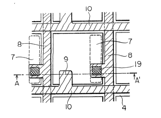
Fig. lA shows a plan view of a photosensor cell 100
used as a photoelectric conversion element. Fig. lB shows a
sectional view of the structure of Fig. lA along the line
A-A', and Fig. 2 shows an equivalent circuit for the
structure. The same reference numerals throughout Figs. lA,
lB, and 2 denote the same parts.
1~7~
In Fi~. 1, a plan view of an aligned array system is
illustrated. In order to improve horizontal resolution, a
pixel shifting (staggered) arrangement can be adopted.
The photosensor cell as shown in Figs. lA and lB
comprises:
A passivation film 2 which is formed of a PSG film or
the like on a silicon substrate 1 and in which an impurity
such as phosphorus (P), antimony (Sb) or arsenic (As) is
doped to obtain a conductivity type of n or n~;
an insulating oxided film 3 consisting of a silicon
oxide film (Sio2);
an element isolation region 4 comprising insulating
films or polysilicon films consisting of sio2 or Si3N4 for
electrically isolating adjacent photosensor cells;
an n~-type region 5 having a low impurity
concentration and formed by epitaxy;
a p-type region 6, which serves as the base of a
bipolar transistor obtained by the doping of an impurity with
an impurity diffusion technique or an ion-implantation
technique;
an n~-type region 7, which serves as the emitter of
a bipolar transistor formed by an impurity diffusion
technique or an ion-implantation technique;
a lead 8 consisting of a conductive material such as
A1, Al-Si, A1-Cu-Si or the like for the external readout of
signals;
an electrode 9 for applying a pulse to the floating
p-type region 6;
a lead lO for the electrode 9;
an n'-type region 11 having a high impurity
concentration and formed by an impurity diffusion technique
or the like on the rear side of the substrate 1 to obtain an
ohmic contact; and
an electrode 12 for providing a substrate potential
and consisting of a conductive material such as aluminum to
provide a collector potential for the bipolar transistor.
A contact 19 shown in Fiy. lA connects the n+-~`ype
region 7 and the lead ~. The intersection of the leads 8 an~
lo is a double-layer structure, in which the leads are
insulated from one another by an insulating region compose~
5 of an insulating material such as sio2, to provide a
bilayered metal wi~ing structure.
A capacitor cox 13 in the equivalent circuit ~hown in
Fig. 2 has a MOS structure consis~ing of the electrode 9, the
insulating film 3, and the p-type region 6 . A bipolar
lo transistor 14 consists of the n'-type region 7 as an emitter,
the p-type region 6 as a base, the n~-type region 5 having a
low impurity concentration, and the n~ or n'-type region 1 as
a collector. As can be seen from the accompanying drawings,
the p-type region 6 is a floating region.
The second equivalent circuit shown in Fig. 2 is
expressed by a base-emitter junction capacitance Cbe 15, a
base-emitter p-n junction diode Dbe 16, a base-collector
junction capacitance Cbc 17, a base-collector p-n junction
diode Dbc 18, and current sources 19 and 20.
The base operation of the photosensor cell will be
described below with reference to Figs. lA, lB and 2, and
involves a charge storage operation upon light reception, a
read out operation, and a refresh operation. In the charge
storage operation, the emitter is grounded through the lead
8, and the collector is biased to a positive potential
through the electrode 12. The base is set to a negative
potential, i.e., reverse biased with respect to the emitter
region 7 by applying a positive pulse voltage through the
lead 10 to the capacitor Cox 13. Biasing to the negative
potential of the base 6 by application of a pulse to the
capacitor Cox 13 will be described in detail with reference
to the refresh operation below.
When light 20 becomes incident on the photosensor
cell shown in Fig. lB, electron-hole pairs are generated in
the semiconductor. Since the n-type region 1 is biased to a
positive potential, electrons flow to the side of the n-type
1~78~
-- 8
region 1. However, holes are stored in the p-type region 6.
When holes are stored in the p-type region 6 in this manner,
the potential of the p-type region 6 gradually changes toward
a positive potential.
Referring to Figs. lA and lB, the lower light-
receiving surface of each cell is mostly occupied ~y a p-type
region and is partially occupied by the n+-type region 7.
Naturally, the concentration of electron-hole pairs which
are photo-excited increases toward the surface. Therefore,
many electron-hole pairs are excited by light in the p-type
region 6. If electrons photo-excited in the p-type region
flow without recombination and are absorbed by the n-type
region, holes excited by the p-type region 6 are stored and
move the region 6 to a positive potential. If the impurity
concentration in the p-type region 6 is uniform, photo-
excited electrons flow to the p-n~ junction between the p-
type region 6 and the n~-type region 5. Thereafter, the
electrons are absorbed in the n-type collector region 1 by
drift due to a strong electric field applied to the n~-type
region. Note that electrons in the p-type region 6 can be
transferred by diffusion alone. However, if the impurity
concentration of the p-type base is controlled to increase
from the surface to the inside, an electric field given by:
Ed = (lJWB) (kT/q) ln (NAs/NAi)
(where WB is the depth of the p-type region 6 from the light-
incident surface, k is the Bolzmann's constant, T is the
absolute temperature q is the unit charge, NAs is the surface
impurity concentration of the p-type base region, and NAi is
the impurity concentration at the interface between the p-
type region 6 and the n~-type high-resistance region 5~
directed toward the surface from the inside of the base is
formed in the base due to the impurity concentration
difference.
If we assume that NAs/NAi > 3, transfer of electrons
in the p-type region 6 is performed by drift in place of
diffusion. In order to effectively obtain carriers photo
1~7~ 0
excited in the p-type region 6 as a signal, the impurity
concentration of the p-type region 6 preferably reduces from
the light-incident surface to the inside. When the p-type
region 6 is formed by diffusion, the impurity concentrati~r
reduces from the surface to the inside.
A portion of the sensor cell below the light-
receiving surface is partially occupied by the nt-type region
7. Since the depth of the n'-type region 7 is normally about
0.2 to 0.3 ~m or less, the amount of light absorbed by the
n'-type region 7 is not large and does not present a problem.
However, for light having short wavelengths, in particular,
for blue light, the presence of the n+-type region 7 may
lower ~ensitivity. The impuri~y concentration of the n+-type
region 7 is normally designed to be about 1 x 102 cm~3 or
more. The diffusion distance of holes in the n~-type region
7 in which an impurity is doped to a high concent~ation is
0.15 to 0.2 ~m. Therefore, in order that holes photo-exclted
in the n+-type region 7 may effectively flow into the p-type
region 6, the n -type region 7 also preferably has a
structure wherein the impurity concentration decreases from
the light-incident surface to the inside. When the impurity
concentration of the n+-type region 7 is as described above,
a strong drift electric field directed from the light-
incident surface to the inside is generated, and holes photo-
excited in the n~-type region 7 immediately flow into the p-
type region 6. When the impurity concentrations of the ni-
type region 7 and the p-type region 6 decreases from the
light-incident surface to the inside, carriers photo-excited
in the n+-type region 7 and the p-type region 6 at the light-
incident surface side of the sensor cell all serve togenerate a photo signal. When the n~-type region 7 is formed
by impurity diffusion from a silicon oxide film or a
polysilicon film in which As or P is doped in a high
concentration, an n~-type region having a preferable impurity
concentration profile as described above can be obtained.
1~7~
-- 10 --
Upon storage of holes, the base potential changes to
the emitter potential and then to ground level where i~ is
clipped. More specifically, the base-emitter path is
forward-biased, and clipped at a voltage at which the holes
stored in the base begin to flow to the emitter. The
saturation potential of the sensor cell is approximately
given by the potential difference between the ground
potential and the bias potential, which is used to bias the
p-type region 6 first to a negative potential. If the n -
type region 7 is not grounded and a charge is stored by aphoto input in the floating state, the p-type region 6 can
store the charge to a potential which is substantially the
same as that at the n-type region 1. In the MOS sensor,
fixed pattern noise due to variations in the parasitic
capacitance of a switching MOS transistor for external read
out, and random noise due to a high wiring capacitance or an
output capacitance are high, and a satisfactory S/N ratio
cannot be obtained. In the photosensor cell of the
structure shown in Figs. lA, lB and 2, the voltage stored in
the p-type region 6 is externally read out. Since the
voltage is relatively high, fixed pattern noise and random
noise due to output capacitance is reduced relative to the
high voltage, and signals with an excellent S/N ratio can be
produced.
Another advantage of the photosensor cell of the
above configuration is a provision of non-destructive read
out of holes stored in the p-type region 6 due to a low
recombination rate between electrons and holes in this region
6. When a voltage VR applied to the electrode 9 during read
out is returned to zero volts, the potential of the p-type
region 6 is reverse-biased as before application of the
voltage VR. Thus, the stored voltage VR generated before
light irradiation is maintained unless another light
irradiation is performed. When the photosensor cell of the
above configuration is used to constitute a photoelectric
conversion device, this capability of non-destructive read
~ 7 ~ O
outs provides the potential for new systems having new modes
of operation.
A time for wh-ch the stored voltage Vp can be stored
in the p-type region 6 is very long, and the maximum storage
time is limited by a dark current which is thermally
generated in a depletion layer at the junction. This is
because the photosensor cell is saturated by a thermally
generated dark current. However, in the photosensor cell of
the configuration described above, the region of the
o depletion layer is the n~-type region 5, having a low
impurity concentration such as about lO12 cm~3 to lo1~ cm~3; it
has a very good crystallinity and only a small number of
electron-hole pairs are thermally generated as compared to a
MOS or 5CD sensor. The dark current is therefore lower than
other conventional devices, and the photosensor cell of
above-described configuration has low noise.
Refresh operation of the charge stored in the p-type
region 6 will now be described. In a photosensor cell of the
configuration described above, the charge stored in the p-
type region 6 is held unless it is removed. Therefore, in
order to input new optical information, a refresh operation
for erasing the previous charge is required. At the same
time, the potential of the floating p-type region 6 must be
charged to a predetermined negative potential.
As in the case of a read out operation, a refresh
operation is performed by applying a positive voltage to the
electrode 9 through the lead l0. The emitter is grounded
through the lead 8. The collector is set at the ground
potential or at a positive potential through the electrode
12.
Fig. 3A is a graph showing read out voltage and read
out time as a function of storage voltage. Fig. 3B is a
graph showing read out time as a function of bias voltage.
Fig. 4A is an equivalent circuit diagram of the refresh
operation, and Fig. 4B is a graph showing base voltage as a
function of r~fresh time.
~7~ 0
- 12 -
As described above, the basic structure of the
photosensor cell of the above configuration is simpler than
those disclosed in Japanese Laid-Open Patent Gazettes Nos.
150878/1981, 157073/1981 and 165473/1981. The structure
allows high-resolution applications which are feasible in the
near future while it also maintains advantages of
conventional structures such as low noise, high output, wide
dynamic range, and non-destructive read out.
An embodiment of a photoelectric conversion device
having two arrays of photosensor cells will be described
below. Fig. 5 shows the configuration of a circuit of a
photoelectric conversion device having a two-dimensional
array (matrix) of basic photosensor cells.
The device has basic photosensor cells 30 (the
collector of the bipolar transistor is connected to the
substrate and the substrate electrode) an example of which is
surrounded by a dotted line; horizontal lines 31, 31',
31",..., for applying read out pulses and refresh pulses; a
vertical shift register 32 for generating read out pulses;
buffer MOS transistors 33, 33', 33", ....... , between the
vertical shift register 32 and the horizontal lines 31, 31i,
31" ...,; a terminal 34 for applying pulses to the gates of
the transistors 33, 33', 33" ...,; buffer MOS transistors 35,
35', 35", ..., for applying refresh pulses; a terminal 36 for
applying pulses to the gates of the transistors 35, 35', 35",
...,; a vertical shift register 52 for applying refresh
pulses; vertical lines 38, 38', 38", ..., and 51, 51', 51"
..., for reading out stored voltages from the basic
photosensor cells 30; a horizontal shift register 39 for
generating pulses so as to select the respective vertical
lines; gate MOS transistors 40, 40', 40", ..., and 49, 49',
49" ..., for enabling or disabling the respective vertlcal
lines; output lines 41 and 59 for reading out the stored
voltages to an amplifier section; MOS transistors 42 and 53
for refreshing the charge stored on an output line; terminals
43 and 54 for applying refresh pulses to the MOS transistors
~;~7~ 0
- 13 -
42 and 53, transistors 44 and 55 (e.~., bipolar, MOS, FET, J-
FET transistors) for amplifying output signals; terminals 46
and 57 for connecting load resistors 45 and 56 and the
transistors 44 and 55 to a power source; signal output
terminals 47 and 58; MOS transistors 48, 48', 48", ... , and
50, 50', 50", ..., ~`or refreshing the charges stored on the
vertical lines 38, 38', 38", ..., and 51, 51', 51", ...,; and
a terminal 60 for applying pulses to the gates of the MOS
transistors 48, 48', 48", ..., and 50, 50~, 50~, ...
The image sensing apparatus comprises a clock driver
CKD for supplying drive pulses to the respective portions 32,
34, 36, 39, 43, 54 and 60 of the photoelectric conversion
device, and a clock generator CKG for supplying timing pulses
to the clock driver CKD. The clock driver CKD and the clock
generator CKG constitute the control means.
Fig. 6 is a diagram showing the method of driving the
apparatus by the control means. In odd fields, line data 11
and 12 forms horizontal scanning line nl, line data 13 and 14
forms horizontal scanning line n2, and line data 15 and 16
form horizontal scanning line n3. In even fields, line data
12 and 13 form horizontal scanning line ml, line data 14 and
15 form horizontal scanning line m2, and line data 16 and 17
form horizontal scanning line m3.
Line data of two horizontal lines is simultaneously
read out, and the read out data appears at the output
terminals 47 and 58.
Fig. 7 shows a first configuration of image sensing
apparatus utilizing a photoelectric conversion device 100 as
shown in Fig. 5 and providing edge correction. It comprises
a switch circuit 68 for inputting the two line signals from
the device 100 to different terminals 72 and 73 for each
field, a subtractor 69, a level adjustment resistor 70, and
an adder 71. Such an arrangement is also applicable to a
conventional X-Y address type MOS image sensor.
In an odd field, an edge signal is obtained in block
APC by subtracting an output at the terminal 47 from an
1;~78~tt
output from the terminal 58. After the level of the edge
signal is adjusted by the resistor 70, it is added to the
original signal from terminal 47 by the adder 71 so as to
obtain an edge-corrected video signal. In an even field, the
output from the terminal 58 is subtracted from that from the
terminal 47 to obtain an edge signal. After the level of the
edge signal is adjusted by the resistor 70, it is added to
the original signal from terminal 58 by the adder 71.
The clock driver CKD switches the switch 68 for each
field. Edge correction can be performed without using a
delay circuit, using the very simple circuit shown in block
APC in Fig. 7, which provides an edge signal generation block
acting as a processing means or an edge signal generating
means which provides a differentiated correction signal.
Fig. 8A is a block diagram showing a further
embodiment of processing means. The embodiment uses a
photoelectric conversion device which is generally similar to
that of Figure 5 except that it simultaneously reads the line
information of three horizontal lines.
Certain of the same reference numerals as are used in
Fig. 5 are used to denote similar parts in Fig. 8A. In Fig.
8A, the clock driver circuit CKD also controls a switch
circuit lO1.
Fig. 8B shows waveforms of the signals f(a), f(b),
f(c) and f(d) at the correspondingly identified points a, b,
c and d of the circuit shown in Fig. 8A. Plots a to _ show
the waveforms in odd fields; d', the output waveform from an
adder 65 in an even field; and d", a double differentiated
edge signal in a frame image, equal to d + d'.
The signal f(d) (plot d in Figure 8b) at point d in
Figure 8A is the second differential of the signal f(c) (plot
c in Figure 8b). By mathematical definition, the first
differential df(c)/dt of signal f(c) at the terminal c is
provided by the following expression:
35 df(c)/dt = lim f(c)-f(c+~t) /~t............ (l)
~t~0
1;~78~;~0
- 15 -
and its second differential is as follows:
d2f(c)/dt = lim ~L ( ) ( 4t)
... ....... (2)
in which f(c+~t) and f(c+2bt) are signals at time lags at and
24t respectively from the signal f(c). If ~t = lH, f(c+~t)
and f(c+2~t) can be replaced with f(b) and f(a) respectively,
that is, f(c+~t) = f(b) and f(c+2~t) = f(a), and expression
(2) becomes:
d f(c)/dt = lim {(f(c)-f(b))-(f(b)-f(a))~ t)2
= lim r 2 f(b)-(f(a)+f(c))/21 (3)
4t~0 1 2
L (4t)
Because ~t = lH~0, d2f(c)/dt2 approximates to a slope of the
first differential for a section ~t, that is,
d2f(c)/dt2 _ 2 _ ~f(b)-(f(a)+f(c))/2~ -------(4)
(~t)
which in turn evaluates to:
_ _2 2 f(d)
(~t)
since f(b)-(f(a)+f(c))/2 is the function performed by the
circuit formed by the parts 64, 65, 66 and 67 in Figure 15a.
Moreover~ is a constant, so that the signal f(d) at
(~t)
terminal d is proportional to the second differential of the
signal f(c).
Signals, successively delayed by lH intervals, for
producing an edge emphasized signal as discussed above and
as graphically illustrated in Figure 15B could be obtained
using lH delay lines 60 and 61 as shown in Figure 15A. The
function f(b)-(f(a)+f(c))/2 is performed by adders 63, 65 and
66, a coefficient circuit 64, and a level adjustment resistor
67.
In Fig. 15B, plots a to d show waveforms of signals
in odd fields; plot d', an output from the adder 65 in even
-- 16 --
fields; plot d", an edge signal of a frame lmagei ~nd plot
e", an edge emphasize~ signal of a frame image.
The arrangement of Figure lsA has the disadvantage
that two expensive delay lin~s mus~ be used, and the circuit
configuration becomes complex. Since signals delayed by
successive lH intervals are avai:La~le simultaneously in the
arrangement of Figure 8A, these disadvantages can be avoide~.
Fi~. g is a diagram showing the wiring of output
lines of the photoelectric conversion device 100 and the
lo method of read out of these lines by the clock driver.
In this embodiment, in an odd field, the clock driver
simultaneously reads out lines 11 to 13 as the horizontal
scanning line nl, then lines 13 to 15 as the horizontal
scanning line n2, lines 15 to 17 as the horizontal scanning
15line n3, and lines 17 to 19 as the horizontal scanning line
n4.
In an even field, the clock driver simultaneously
reads out line 12 to 14 as the horizontal scanning line ml,
lines 14 to 16 as the horizontal scanning line m2, and lines
2016 to 18 as tne horizontal scanning line m3.
Fig. 10 shows the internal functions of the switch
circuit 101 for establishing correspondence between output
terminals 01, 02 and 03 of the device 100 and outputs a, _
and c of switch 101 as in Fig. 8A. The clock driver CKD
switches the outputs in combinations which are different for
each field and each line, as shown in Fig. 11. Since the
switch circuit 101 is disposed between the device 100 and the
circuit APC as shown in Fig. 8A, an edge compensation circuit
need only be incorporated for one combination of the outputs
a, b and c as shown in Fig. 8A, so that the overall
construction is simplified.
Fig. 12 is a block diagram showing a further
embodimen~. ~he apparatus has adders 74, 76, 78 and 83,
weighting circuits 75 and 79, a level adjustment resistor 77,
a switch circuit 80, an intensity signal processing circuit
81, and a color signal processing circuit 82.
- ~7 -
In this embodiment, as i.n the previous embodiment,
edge correction can be performed without using ~elay lines or
the lik~, but the configuration of the switch circuit 80 can
be simplified. In addition, only one series of parts 75 and
79 is required, and the wiring in the device 100 can be
simplified. In this case the various switching combinations
as shown in Figure 11 can be achieved by the action of
switching circuit 80, which selects one of the signals 01, 02
and 03, the amplitude of the selected signal being increased
by 50~ so as to cancel the component of that signal in the
output of the divider 75. The end result is the same as that
produced by the circuit of Figure 8A, but the switching is
much simpler.
Fig. 13 shows how the switching operation of the
switch circuit 80 can be controlled. of three horizontal
lines simultaneously read, the central horizontal line is
handled as an original signal, and the upper and lower line
signals correspond to signals relatively delayed and advanced
by lH, respectively.
Thus by simultaneously reading a plurality of lines
of a photoelectric conversion device, the signals from a
plurality of lines are immediately available to generate an
edge-corrected signal, greatly simplifying the signal
processing system. A switch circuit is provided for changing
the combination in which the plurality of line signals are
supplied to a processing circuit so that only a single
processing circuit is required, and the overall configuration
is simplified. Connections within the photoelectric
conversion device are also simplified.
When a photoelectric conversion device capable of
non-destructive read out is used, three or more horizontal
lines can be simultaneously read out, whilst the signals can
be read out in partially overlapped groups upon each
horizontal scan, thereby improving vertical correlation. An
edge signal of the second order or greater can be obtained.
The switching circuit can be incorporated in the
1~78tji~0
- 18 -
photoelectric conversion device.
since the vertical correlation distance is ~mall,
inclusion of a false signal is rare. By providing a
switching circuit for switching the output lines of the
photoelectric conversion device, the construction of the edge
signal generating means and the photoelectric conversion
device can be simplified.
Fig. 14 shows an arrangement such that a defective
pixel in a photoelectric conversion device can be corrected.
The same reference numerals used in Fig. 13 denote the same
parts in Fig. 14.
The apparatus shown in Fig. 14 has an adder 84, a
weighting circuit 85, a switch 86 as a switching means, a
subtracter 87, and a ROM storing the position of a defective
pixel. The parts 84 to 87, 66, 67, and the like constitute
an edge correction processing means.
A switch circuit 101 converts the three horizontal
line signals read out from output terminals 01, 02 and 03 of
the device 100 to obtain signals a, _ and c as in Fig. 11.
The signal k is the middle of the three horizontal lines read
out simultaneously from the photoelectric conversion device.
It is assumed for purposes of illustration that the signal _
contains a dropout at a predetermined pixel position.
The position of the defective pixel is prestored in
the ROM 88. The ROM 88 is driven by a sync signal from a
clock generator CKG. The switch 86 is switched from a
position x to a position y at the position of the defective
pixel. With the switch in the y position, the signal _ is
replaced by a signal which is an average of the signals a and
c. The adder 84 and the weighting circuit 85 form the
average signal. The average signal is also subjected to
subtraction at the subtracter 87 to form an edge signal _.
Operation is otherwise the same as that previously described.
Correction of a defective pixel can thus be performed without
using a delay line, whilst the circuit configuration can be
simplified, and the image quality improved. The
'. ' '
' ~
t~
- 19
manufacturing yield of the photoelectric conversion device
can also be improved. Dropouts of the signal b could be
directly detected, and the switch 85 driven directly.
A defective pixel can thus be corrected by a simple
circuit, and is replaced by a signal derived from adjacent
pixels having high correlation.