Note: Descriptions are shown in the official language in which they were submitted.
~7~
SPECIFICATION
TITLE OF THE INVENTION
Pay televiosn system.
BACKGROUND OF TE~E INVEMTION
FIELD OF THE INVENTI~N
This invention relates to a pay television system of using
unidirectional television signals as in television broadcasting
using a broadcasting satellite, and more particularly to a
charging system of its receiving charge.
DRSCRIPTION OF THE PRIOR ART
In a unidirectional signal transmisstion and receiving
system as in a sa-tellite television broadcasting, to collect
a receiving charge at a terminal receiver as in the case of
receiving a charged program of CATV, it is necessary to have
the receiving charge paid by the subscribers on a "pay later"
basis, and to disable the terminal receiver of -the subscriber
who does not pay.
This is practiced in a pay television of bidirec-tional
CATV system.
In the case o~ CA'I'V system, however, subscribers must
apply for viewing a specivied pay television program to the
transmission center by the up line of the bidirectional
communication lines or by telephone, and such method cannot be
employed in the unidirectional system such ~s satellite
broadcasting. And in this method, when many subscribers apply
for a same program at the same tlme to the center, an overflow
of the capacity of the telephone line or overflow of the
processing capacity at the receiving side occurred.
BRIEF DESCRIPTION OF T~IE DRAWINGS
Fig. 1 is a block diagram of a pay television system in
one of examples of the prior art; Fig. 2 is a block diagram
of a satellite television broadcasting system for realizing
the pay television system of this invention; Fig. 3 is a
waveform diagram of video signal in the same system; Fig. 4
is a block diagram of a receiver used in a pay television
system in one of the embodiments of this invention; Fig. 5,
6 are waveform diagrams of ~ignals used in the same receiver;
Fig. 7 is a block diagram of an amount memory used in the
same receiver; Fig. 8 is a block diagram of a receiver used
in a pay television system in a dif f erent embodiment; Fig. 9
is a block diagram of ~ey code processing circuit used in
the same receiver; and Fig- 10 is a chart of signals used in
the same receiver.
An example of Suc}l conventioanl composition is shown in
Fig.~l, in whlch numeral 1 is a computer center of a CATV
station for controlling the record of payment of receiving charge
hy the subscribers, selection of programs to be transmitted
according to the request of the subscribers, compilation of
~;~78~
control codes, and others while a CATv center 2 transmits the
video signals prepared by VTR, film or at the studio according
to its computer commands, together with said control codes.
Reference number 3A is a head-end for signal transmission,
and sends out plural television signals from the CATV center
2 in a form of, for example, mid-band television signals of
V~F. Reference number 3B is a buffer circuit for receiving
up signals from each receiving terminal, and the head-end 3A
and tuner/converter 4 at the receiving terminal side of C~TV
and buffer circuit 3B are connected by a same cable or
different cables. Or a telephone line may be used instead
of the cable for up signal from the tuner/converter 4 to the
- 3a -
~27~3~S~i
buffer circuit 3B.
Numeral 4 is a terminal side tuner or converter for
frequency conversion of mid-band signals lnto a first-channel
(or second-channel) signals of VHF, and one channel is CATV
signals of the mid-band is converted into one channel of
VEIF by the command from a key pad 5. Incidentally, when the
CATV signal is scrambled, it is once converted into a base
band signal, and descrambled, then converted into an RF
signal again to be delivered as signal of one channel of VHF.
Numeral 6 is a television receiver for VHF band
reception. The viewer applies for a desired program (charged)
to the computer center 1 by operating the key pad 5 or through
telephone set 7. At the center 1, the charge is set at
every terminal. Or when sending out signals by scrambling,
the descrambling key code is transmitted in the sequence of
center computer 1, CATV center 2, head-end 3, and converter/
tuner 4. At the tuner/converter 4, the received signals
are descrambled by using this key code, and NTSC video
signals of normal pic-ture are reproduced, and are converted
into one channel of VHF to be supplied into the television
receiver 6. There are multiple tuners/converters 4 to
telephone sets 7 which are terminal stations, and a central
intervenes between the telephone set 7 and telephone interEace
8. At the telephone interface 8, generally, an opera-tor
- 4 -
hears the request from each terminal, and it is converted
into the format of input to the center computer 1. This is
an example of the prior art.
OB~ECT OF THE INVENTION
This invention is to present a system to realize a pay
television system in a unidirectional television signal
transmission such as satellite television broadcasting system.
More particularly, it is intended to present a pay television
system capable of effectively preventing illegal access to
the program having hard-to-read key codes.
BRIEF OF THE INVENTION
This invention, relating to a unidirectional television
system such as satellite television broadcasting system, is
intended to transmit and receive the charging information
corresponding to the content of the program being transmitted
in the digital form at certain time in-tervals, and account
the amount by a charging amount accounting means built in
the receiver from said information and the time of receiving
the television program, write the charge data proportional
to the amount in a memory, read out the charge data in the
memory when necessary, and display it on a display means.
Also in this invention, when the charge information of
each terminal is sent from the television ~rogram
transmission side at every terminal, this charge information
is transmitted to a memory, and is compared with the charge
information preliminarily stored in the memory, and only when
the both amounts agree or the charge sent from the transmission
side is larger than the charge in the memory, a new key code
sent from the transmission side is stored so that the
television program may be received.
Moreover, in this invention, the memory is divided into
three sections, and the charge information proportional to
the receiving time of every program is stored in the first
memory, the content of the first memory is added to the
content of the second memory at every termination of reception
of a pay program, such as when the program ends, the power
is Cllt off, or the channel is changed, and the content of
the second memory is transferred and stored in the third
memory when receiving the charge display indication code
sent out from the transmission side at every time interval.
When receiving the data corresponding to the paid charge
individually sent from each receiver from the transmission
side, the data is compared with the content of the first or
second memory, when the two are equal or the content of the
second or third memory .is smaller than the received data,
the contents of the second and third memories are cleared,
!38~i~
and when the received data is smaller than the content of
the second or third memory, the balance is stored in the
second and third memories, and the amount of this balance is
displayed.
Furthermore, in this invention, the memory for storing
the charge information, and the memory for storing the key
code signal for descrmabling the scrambled video signal and
sound signal are separately provided. As the key code signal
memory, the first memory for storing the presently effective
key code and the second memory for storing the key code
signal which becomes effective in the future are provided,
and by storing the key code siynals into them, the key code
signals continuously sent from the transmission side are
written once into the memory. Besides, there is another
memory for storing flags indicating the rewriting data and
the type of charge information at that time according to the
charge information of individual terminals as the content
of the charge information memory is sent from the transmission
side, and by the key code changeover signal from the second
memory, the transfer of the content of the second memory into
the first memory is stored in this third memory.
Still more, in this in~ention, while the individual
addresses assigned to every terminal are scrambled by a
first scrambling method to be skored in the memory, the
-- 7 --
..
information for descrambling the terminal key code scrambled
by a second scrambling method is scrambled by the first
scrambling method and stored in the memory, and the program
for descrambling this first scrambling method is stored in the
memory, such as ROM, on the chip of a microprocessor for
main control.
Eventually, key codes may be transmitted in different
scrambling method to different terminals, so that illegal
access to pay program may be effective prevented.
-- 8 --
..
DESCRIPTION OF THE PREFERRED EMBODIMENTS
The embodiments of the present invention are Eurther
described below in conjunction of the accompanying drawings.
One of the embodiments of the present invention is shown
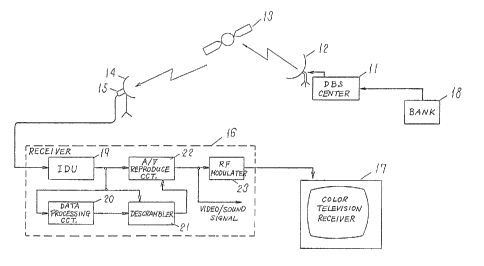
in Fig. 2, in which numeral 11 denotes a transmission center
of satellite broadcast, being generally called a DBS center.
Numeral 12 is a large-sized parabolic antenna for sending
out signals to a geostationary satellite 13 which is a
repeater for retransmitting the signal sent from the earth
back to the earth. Numeral 14 is a receiving antenna
installed at a receiver terminal on the ground. Numeral 15
is a low noise converter, and it converts, for example, the
television broadcast signal of 12 GHæ ban received by the
antenna 14 into one of 1 GHz band, and transmits it to a
receiver 16 as a first IF signal.
Numeral 19 in the receiver 16 is called an IF demodulator
unit (IDU), and it converts, for example, the first IF input
of 1 GHz band into a second IF signal of 400 MHz, and
amplifies and detects it, and delivers a base band signal.
Numeral 20 is a data processing circuit for picking up
digital signals from the output, processing and feeding to
a descrambler 21.
Suppose, for instance, that the video signal is
scrambled by synchronism shiEting and video component random
inversion while the sound is scrambled by digital sound with
the bit arrangement changed at random. When the output of
the IDU 19 is directly projected on the CRT of the color
television receiver 17, the luminance is inverted on the
screen, and the horizontal and vertical de-flections cannot
be synchronized, so that the picture is destroyed and
unintelligible. Or when the sound is directly delivered
from the speaker, it is a mere noise. Accordingly, the
descrambler 21 changes over inversion or noninversion of the
picture depending on -the output from the data processing
circuit 20, and the bits of the digital signal of sound are
rearranged to descramble to normal picture and sound. At an
A/V reproducing circuit 22, only the horizontal blanking
period of the output from the IDU 19, that is, only the 3
portion tl to t2 in Fig. 3 B is varied in the DC level, and
is synthesized with the portion t2 to tll of the output of
descrambler 21 (Fig. 3 C), and the original video signal
(Fig. 3 A) is reproduced, and the digital sound signal of the
output of descrambler 21 is converted to an analog sound
signal.
The output of this A/V reproducing circuit 22 ls
converted into a signal Gf a proper channel of V~IF band in
an RF modulator 23, and when its output is fed to the antenna
input of an ordinary color television receiver 17, the scrambled
picture and sound are received in a normal descrambled state.
Such program to be received by returning scrambled
- 10 -
picture and sound to normal picture and sound is often a
charged program. If charged, the mount of charge is indicated
by the digital signal for control superposed in the vertical
blanking period (VBL) of the video signal of the program, and
the charge is recorded in the memory of the receiver.
Generally, when a certain program is received for 2 to 10
minutes or more, the charge for the entire program will be
billed.
As a method of payment of the charge, for example, a
card reader is attached to the data proeessing circuit 20 in
Fig. 20, and a purchased card (such as a season ticket~ is
inserted into it, and the control signal for descrambling to
the descrambler 21 is sent out from the data processing circuit
20 only for the time corresponding to the paid amount. Or,
in other method, the charge is prepaid to a bank 18, and
according to this prepaid eharge data, a eode expressing the
paid-in charge is sent from the DBS center 11 to eaeh terminal
(where an address is provided individually) through the
geostationary satellite 13, and its eharge code is written in
the memory at the terminal and the charge code in the memory
is ehanged (decreased) every time charge program is received
at the terminal, and when the remainder becomes zero, the
charge is paid again to the bank 18 and the same procedure
is repea-ted.
More specifically, the content of the data processing
~;Z7~35~
circuit 20 in Fig. 2 is composed as indicated by numerals
31 to 50 in Fig. 4, and when a charged program is received,
the charge corresponding to the receiving time is calculated
at the terminal side according to the charge data superposed
in the VBL period of the video signal and is written into
the nonvolatile memory, and the subscriber pays the viewing
charge equal to or more than the amount received within the
month to the bank every month. At the center, the signal
indicating the paid-in amount is sent to each terminal (at
every address) from the DBS center 11 by polling, and at
the individual terminal the content of the memory 47 is
decreased by the portion of the amount indicated by that
amount signal, and the receiver is controlled so that charged
programs may not be received from the ne~t month unless the
content of the memory 47 is canceled to zero.
In Fig. 4, numeral 31 is a waveform forming circuit
which shapes the waveform of data signal, such as Fig. 5 A
signal, superposed in the VBL period in the output of the
IDU 19, and composes a pulse waveform signal as shown in
Fig. 5 B. Numeral 32 is a clock detecting circuit which,
using iterative clock run signals CR of "1" and "0" signals
of 2 bytes in the head portion of Fig. 5 B, reprocluces clock
pulses synchronized with them, detects a framing code at the
8th bit of framing code signal FC within the reception signal
to establish frame synchronizing, and synchroniæes the
- 12 -
~'7~
sampling clock generated in a sampling clock generating
circuit 33 to the reception signal. Numeral 33 is a circuit
to form a sampling clock of thus controlled appropriate phase.
Its output is divided by a main clock forming circuit 34 to
compose a main clock to drive the work RAM 37, work ROM 38,
center processing unit (CPU) 39, etc.
The clock synchronized with each bit of the reception
signal from the output of the sampling clock generating
circuit 33 is fed to the sampling circuit 35, and each bit of
the reception signal is sampled. The pulse wid-th of each bit
of reception signal is about 175 ns at 5/8 fsc and in this
cycle time it is difflcult to operate the work RAM 37 to CPU
39 in Fig. 4. When an 8-bit microprocessor is used as the
CPU 39, it is convenient to handle the reception data by
8 bit parallel signals. Therefore, as the sampling circuit
35, a shift register of series input-parallel output type
such as SN74LS164 is suited. When its output is stored in a
latch circuit 36 at every 8 bits on the basis of the 8th bit
of the framing code, the output is an 8-bit paralle] signal,
and varies in the cycle time of 8 x 5/5f = 1.~ ~s. This
cycle time is suited to operation of each circuit. This
output is connected toa bus line 40.
Numeral 37 is a work R~M of CPU 39, and 38 is a work
ROM of CPU 39. The CPU 39 is an 8-bit microprocessor (for
example, MB6809E).
Referring now to control codes CO, Cl to C7 in the
reception signal B in Fig. 5, CO and Cl are iterative clock
run signals CR oE 1 and 0, and C2 is a framing code signal
of 11100101. C3 is composed of information of 4 bits,
humming check code of 3 bits, and parity bit of 1 bit. C~
and subsequent data are all in the same composition in every
byte. The contents of information of C3 and C4 are compiled
Table 1, in which only three kinds necessary for explanation
are shown. Actually, more than several kinds can be considered.
Similar~y, the contents of information of 4 bits of C5 are
yiven in Table 2.
Table 1
L M
~3 B
00000000 Dummy packet
_
10000000 Teletext
01000000 DBS signal
__
11000000 _ __
Spare
11111111
~ _J
C3 C4 _
- 14 -
Table 2
L M
B B
0000 Dummy
1000 Program data
0100 Scrambled data
1100 Address data
0010
. Spare
1111
~
C5 _
In the case of satellite television broadcas~ing,
01000000 is used in 8 bits of C3, C4, and any one of 1000,
0100, 1100 is used in C5.
When the data of 28 bytes in the reception signal as
in Fig. 5 A is program data, an example is shown in Fig. 5 C.
In its beginning portion, the number indicating the kind of
program is expressed in a ~our-digit BCD code in 4 bytes as
the tag-code. Therefore, 9999 kinds can be speci~ied.
The next keyword is a key code which is changed every
month, and it is indispensable for descrambling the signals
received at the terminal side, and the reception at -the
~7~35~
unpaid terminal is stopped by stopping the transmission of
this key code from the DBS center. For example, the payment
data is set on the 20th day every month, and the key code is
changed from the first day of each month. Since th~ receiver
16 in Fig. 2 is always energized and it is operating unless
the power cord is unplugged.
The next charge code contains a four-digit BCD information
in 4 bytes. The charge code varies wi-th the passing of the
time, and the charge proportional to the program viewing
time (the time being displayed on the CRT) is recorded. Its
content is described in details below.
The next PN key is a four-byte (or 16-bit as information~
expression of the initial value of the PN code for descrambl-
ing the scrambled signals. Prevention of illegal access by
PN key is a first measure of security. The next date code,
comprising 2 digits of BCD for the month and 2 digits of
BCD for the day, uses 4 digits of BCD, that is, information
bit x 4 in the four bytes. The time also comprises of 2
digits of BCD for the hour and 2 digits of BCD for the minute.
The content is composed as shown above when the data is
program data packet (C5 is 1).
Meanwhile, when C5 is 2 (00100) and the scrambled data
packet is sent out, all oE 2~ bytes (of which 14 bytes are
information data) are data as shown in C', and 14 bytes of
the information portion of them are written into specified
- 16 -
~`7~ ~ ~7
positions of the work RAM. This data differs in the content
in very program. Various contents and kinds oE scrambled
data may be considered, but they are ommitted in this
description.
Or when C5 is 3 (0011), the address data packet is sent
in 28 bytes as shown in C". This address data packet includes,
as shown in Fig. 5 C", the address indicating two terminals
within one packet. This C' is magnified in Fig. 6, and its
first half 14 bytes are magnified in Fig. 6 D. The
information bits of the first half 7 bytes of D are 28 bits
of the portion of 7 bytes, and 228, or about 268 million,
terminal address can be distinguished.
The latter hald 8 bytes may be divided as shown in
Fig. 6 E, in which E refers only the information bits, that
is, 32 bits of the portion of 8 bytes. The first two bytes
of E (the first one byte in -the case of information only)
are for sending the directions from the DBS center -to the
terminals in the maximum of 255 kinds, and, for example,
when "1" is specified as in Fig. 6, the total amount of the
pay television viewed at the specific terminal up to that
point is indicated. When the amount is given at increments
of 2~ cents each, up to 2 dollars can be specified in the
right-hand 12 bits in Fiy. 6 (the information of 1.5 bytes in
the data area of 3 bytes). Therefore, when clearing the
charge, the code of amount (102~ dollars 75 cents at maximum)
is sent from every termlnal, while the amount paid by the
subscriber to the bank is sent from the DBS center 11 to each
terminal, so that the content in the amount memory 47 at
the terminal is updated. If the amount of viewing the
programs is written in the amount memory 47 in the unit of
25 cents, the amount sent from the DBS center 11 is subtracted
from its content, and when the content in the amount memory
47 becomes zero, it is detected by the CPU 39, and the key
code in Fig. 6 is read in. If the content in the amount
memory 47 does not become zero, that is, if the paid-in
amount is short, the key code is not taken in, so that the
scrambled information (picture, sound) cannot be descrambled
and viewed from the next month. The amount is written (that
is, subtracted from) into the memory 47 once every month,
and the charge data is sent from the DBS center 11 consecu-
tively for about a week each at the end and beginning of a
month. Therefore, if the power source of the receiver is
cut off by mistake, when the power is connected even in a day
within this two-week period, the paid charge can be written
into the amount memory 47 to cancel the content to zero, so
that the key code may be read in. The key code, and entry
of date, time, etc. into the amount memory 47 are written
into a nonvolatile memory 53 as in the case of writting into
the amount memory 47 in Fig. 4. In the memory 53, the data
writing data (time) into the amount memory 47 is written,
- 18 -
A~
and if the amount is paid twice or more by mistake, it is
controlled so that the data may be written correctly into
the amount memory 47 as the first time, second time, and so
forth.
Referring then to key codes, a key code is composed of
12 bits, and represents a formula to determine the 2l2-l PN
series signals. For example, the key code is sent Eorth as
011000010001, the formula becomes xll + x7 ~ x2 ~ x = f(x).
Or this polynominal may contain ll bits or less, instead of
12 bits. Or the key code may contain 16 bits, and the message
in Fig. 6 E may be decreased from l byte to 4 bits.
The actual operation is described below. When a terminal
is purchased, all contents in the buffer circuit 46 in Fig. 4
are zero, and when the power is supplied to this terminal
(suppose X), first the key code is taken in. If this terminal
is purchased in the middle of a month, since periodic polling
to all terminals is not effected by the DBS center 11,
polling of the number of terminals installed on or around
that day (for example, 10,000) is effected temporarily. As
clear from Fig. 6, since two terminals can be polled by lH
(horizontal period), when 5H in the VBL period is assigned
for polling, it results in 10 terminals/field = 600/sec
= 36,000/min, which means polling of newly subscribed
terminals can be e~fected within a minute. Therefore, a newly
purchased terminal can take in the key code of the contemporary
-- 19 --
month within about l minute. When a terminal is installed
at the end of a month, though the key code for the next month
is periodically sent to all subscribers periodically, if,
for example, half of lH of 5H the VBL period is used for
polling of key code of the month for new subscribers, it
becomes (36000/10) x 3 = 10.800 as evident ~rom the
explanation above, and polling of about 10,000 new subscribers
can be finished in about 3 minutes. Supposing the total
number of subscribers at this point -to be 10 million, all
subscribers can be polled in about 61 minutes.
By the way, this terminal X is given its own address in
28 bits. These 28 bits are, in order to prevent illegal
access to charged programs, scattered about, for example, in
the memory comprising 256 bits, or written in part of the work
ROM 38 or in an independent chip so that a correct address
may be obtained by operating the address code of 28 bits
according to the keyword in Fig. 5 C. If, for example,
operated by the keyword, i-t is necessary to receiver the
packet of Fig. 5 C. Considering the data transmission
efficiency, if superposing a same packet in all of 5H at a
rate of once a second and sending out, the keyword is
received within a second at the receiving side, and is
written into the work RAM 37. This keyword has an information
capacity of 16 bi-ts. By operating the data after the
keyword and other data according to the keyword and
- 20 -
~7~
descrambling the scrambled data, a second means of security
(prevention of illeyal accessj may be achieved.
After receiving the keyword, the packet in the ~orm of
Fig. 5 C" is received, and 28 bits of the address of terminal
X are searched. When the address data 28 bits being
transmitted and the address 28 bits in the said work ROM 38
coincide, the eight bytes of Fig. 6 E are taken into the
worm RAM 37. Since the content of the amount memory 47 at
terminal X is zero, MSB of the message in Fig. 6 E and the
bit of one position lower are seen according to the
instruction from the CPU 39. Such program is assembled in
the work ROM 38. The following explanation is given on the
same principle, that is, the CPU 39 conforms to the program
of work ROM 38.
Since the MSB is "1" in the middle of a month (the code
should be assigned so that other bits can be ignored), the
12 bits of the key code are taken into the work RAM 37, and
sent to the nonvolatile memory 53 through the bus line and
stored. ~hereafter, by using this key code, the data of
Fig. 5 C, C', C" are descrambled.
If a received program is a charged one, the charge per
unit time is indicated in the charge code. It is ideal for
the charged program that the charge proportional to the
received duration may be directly billed. As one of the
methods, for example, suppose one 60-minute program costs
- 21 -
6 dollars, and 25 cents is charged for every 2.5 minutes.
In this case, as the charge code, the content of the code is
varied every 2.5 minutes, one bit (corresponding to 25 cents)
is fed to the counters 43 to 45 every time the code is
changed, and the pulses corresponding to the received time
are counted. When the program end data (such as all "l" in
charge code or spare code) is detected, or the receiving
channel is changed, or the power source is cut off, the
output of the counters 43 to 45 (indlcating the multiples of
25 cents) is written into the amount memory 47 composed of
nonvolatile memory through the buffer. The amount memory
47 is a nonvolatile memory including an adder, and has, for -
example, 12 bits. When the power source is cut off, the
counter 43 to amount memory 47 are supported temporarily by
the battery, and the data in counters 43 to 45 is written
into the amount memory 47 through the buffer 46.
In other method, the viewing charge amount from start
of a program till a specific time is sent in codes from the
Dss center 11 every 2.5 minutes, and the balance of the
first received charge code and the final- one is written into
the amount memory 47 at the terminal X. In this method,
every time the charge code varies, the unit charge is
calculated to detect how many multiples of 25 cents, and
pulses corresponding to the number are supplied to the
counter 43 to 45 through the up detection circuit 41 to count
- 22 -
them up.
In either method, at every passing of the time
corresponding to 25 cents, the counters 43 to 45 are counted
up every bit through the up detection circuit 41.
Incidentally, the amount memory 47 may be also composed
as in Fig. 7. That is, possessing two sets of memories 47A,
47B, the content of the buffer 46 is always written into the
memory 47, and when one program is finished (that is, when
the channel is changed, the end code is detected or the power
source is cut off), the content of the memory 47A is added
to the content of memory 47B to be stored in memory 47s, and
when reading out, the data is taken out of the memory 47B.
Next, the PN key is explained. As mentioned above, the
receiver 16 stores 12 bits of the key code. The PN key has
16 bits, of which 12 bits from the least significant bit (LSB~
denote the initial value of the PN series and 4 bits from the
most significant bit (MSB) indicate how many bits the PN
series should be moved from the initial value. By using the
12-bit series obtained by putting the initial value 12 bits
indicated by this PN key as the substi'cute for the initial
value of said polynomial formula and shifting by the number
indicated by said 4 bits, inversion and noninversion of the
video signal are changed over, and the sound signal is
operated and processed (the sound is quantized in 12 blts),
and the picture and sound are descrambled to the original
- 23 -
state.
In other method, meanwhile, the descrambling method of
picture and sound may be varied in every lH by shifting the
PN series obtained by pu-tting the initial value of said 12
bits by one bit each at every lH.
The month, day, and time are stored in the work RAM 37,
and may be used appropriately.
Next, supposing to close the accounting one month later
or on the 10th day every month, the content of the memory 47B
is transferred to the memory 47C (the amount memory 47 is
composed of three memories 47A to 47C). It is designed so
that the transfer may be effected automatically when the charge
display message of Eig. 6 E is received. As the address at
this time, either a number common to all terminals (a special
number) is used, or one of spares is used as the packet of
address "all" at C5. After the charge display message, the
key code and amount code are ignored.
When the charge display message is received, the CPU
39 transfers the content of memory 47B in the amount memory
47 into the memory 47C, and writes the content into the
luminance memory 49 through the buffer 48 and bus line 40.
In this case, since the content of the memory 47C is
converted into a numerical pattern by the work ROM 38 and
CPU 39 and the numerical pattexn is written into the
luminance memory 49, its content is read out along with the
- 24 -
B~
scanning of electron beam of the CRT 52 and fed to the CRT
53 through buffer amplifier 51, so that the charge is
numerically displayed on the CRT. It is sufficient when
the buffer amplifier 51 possesses a function to superpose
the usual program picture and the charge information, or a
function to change over so that only the charge may be
displayed. Numeral 50 is an address circuit for applying
writing and reading addresses to the luminance memory 49.
At the terminal of a subscriber who does not pay the
indicated charge to the bank by, for example, the 20th day
of every month, the amount of the address control data after
the 21st day is set to zero, and the key code is set to zero,
and polling is continued. As a result, when the key code is
changed to a new one on the first day of the next month, the
data cannot be descrambled at this terminal, and the
scrambled picture and sound cannot be rece~ived normally.
Or if the paid amount is short, the key code is sent,
but when the content of the memory 47C is not zero due to
the function of the CPU 39 in the receiver 16, the key code
is not taken into the nonvolatile memory 53, so that
scrambled picture and sound cannot be descrambled. Or, in
the case of payment shortage, it is extremely easy to
indicate the balance to be paid automatically.
An example of charge adjus-tment operation is explained
below by referring to Fig. 4. Counters 43, 44, 45 are CMOS
~7~
counters (for example, 74LS192), and suppose their inputs and
outputs are separately connected to the buffer memory 46.
When the data corresponding to the paid amount is sent from
the DBS center 11, this data is stored in the work RAM 37.
On the other hand, its content is transmitted to the counters
43 to 45 through the buffer amplifier 46 according to the
instruction from the CPU 39. In consequence, the charge da~a
.in the work RAM 37 is divided by 25-cent increments accordin~
to the instruction from the CPU 39, and pulses of integer
multiples of 25 cents are fed to the count-down terminal OL
the counter 43 through the down detection circuit 42, and
the contents in the counters 43 to 45 are counted down by the
number of said pulses. When all outputs of the counters -3
to 45 become zero, it is designed so that the output of the
counters 43 to 45 may not change further. In this state,
the outputs of the counters 43 to 45 are written again into
the amount memory 47, and if, for instance, the outputs of
the counters 43 to 45 are all zero, the key code can be
received also in the next month, and if any one of the
outputs of the counters 43 to 45 is 1, .it is judged that the
payment is in shortage, which is indicated on the CRT 52.
Therefore, the subscriber should either pay for the shortece
or give up the charged program.
In this cons-titution, thus, even in a unidirectional
television such as satellite broadcasting, a charging method
- 26 -
for pay television broadcasting can be effected easily, and
protection from illegal access may be achieved sufficiently.
The composition of the amount memory 47 is describe~
below in conjunction with Fig. 7, in which memory 47A is for
storing the charge of the pay television program viewed to
that meoment, and memory 47B is for storing the cumulative
total of the charges. As mentioned above, when stopping
receiving the program, the charge data of the program is
added from the memory 47A to the adder 47E according to the
instruction from the write/read control circuit 47D, and is
added to the content of the memory 47B, and the added result
is newly stored in the memory 47B.
When billing -the charge in one month unit, a message
indicating the key code for the next month as in Fig. 6 F is
detected, and by this detection output, reading from the
wxite/read control circuit 47D into the memory 47B and
clearing of its content are instructed, and the content is
transferred from memory 47B to memory 47C. The content of
memory 47B becomes zero right after it is transferred to the
memory 47C, and it begins to store the charge of pay programs
of a new month. The write/read control circuit 47D and adder
47E are controlled by specific address in 16 bits of the
address signal by the CPU 39.
For prevention of illegal access, meanwhile, part of
the program of the content of work ROM 38 may be put into
~L~7~3~5~-~
the CPU 39 to be customerized, or the work ROM 38 may be
divided into two sections and only the address may be set in
fuse ROM so that the content of the fuse ROM may be varied
for each terminal, or if the program quantity is small, it
may be wholly written into the ROM sinde the CPU 39.
As a different embodiment, an example of using an amount
accounting circuit is shown in Fig. 8.
In this embodiment, every time the charge code varies
every 2.5 minutes, the content of the charge memory in the
work RAM 37 is added by one bit each (corresponding to 25
cents), and the data of charge information is supplied from
the work RAM 37 to the memory 47A in the amount memory ~7
to increase the data of the charge memory in the work RAM 37
by the number of bits corresponding to the time of viewing.
When the program end data (when all charge codes are "1" or
spare code is used), or when the receiving channel is
changed, or the power source is cut off, 37 to 47 are tem-
porarily supported by the battery, and the output of the
memory 47A (whlch indicates multiples of 25 cents) is supplied
to the addition/subtraction register 47E and added to the
content of the memory 47B, and the added result is written
again into the memory 47s.
The nonvolatile memory block of amount memory 47 is
composed of three memories 47A, ~7B, 47C of 12 bits each.
If the output of the flag register 47F is "a0, al, 1" which
- 28 -
indicates addition, the addition/subtraction register 47E
performs addition. By supporting the circuits of 37 to 47
by the battery for a short time, the charge information of
the work RAM 37 is written into the memory 47A, and the
content of memory 47A and the content of memory 47B are added,
and the obtained result is written into the memory 47B.
In other method, for example, the charge code of the
cumulative amount from the start of a program to a specific
moment is sent from the DBS center 11, for example, every
2.5 minutes, and the balance of the first received charge
code and the final one is calculated at the terminal X by
means of the CPU 39, work ROM 38 and work RAM 37, and is
written into the memory 47A, and when the program is over,
the content in the memory 47A is added to the content in
the memory 47B, and the sum is written into the 47B~ In
this case, every time the charge code varies, the unit
charge is calculated, and multiples of 25 cents are calculated,
and the content of the charge memory in the work RAM 37 is
increased by the number of multiples, and the increased
result is written into the memory 47A every time.
In either method, the content of the memory 47B is
increased by~one bit each at every time corresponding to
the worth of 25 cents.
In another me-thod, the amount memory 47 is composed
of, as shown in Fig. 8, nonvolatile RAMS ~7A, 47~, 47C of 12
29 -
bits each, and the content of the charge memory in the work
RA~l 37 is written into the memory 47A. When one program is
over (that is, when the channel ls changed, the end code is
detected, or the power source is cu~ off), the content of
the memory 47A is added to the content of the memory 47B to
be stored in memory 47B, and when reading out, it is taken
out from the memory 47B.
An example of charge settling of this system is shown
below. When the data corresponding to the paid charge E is
sent from the DBS center 11, this data is stored in the work
R~M 37. Prior to this, the content of the memory 47B has
been transferred to the memory 47C according to the instruction
from the work RAM 37, but the content of the memory 47s
until the time of payment includes the amount for the pay
programs viewed after the closing of account of the previous
month till the data from the DBS center is received, and the
content ~the numerical value) of the memory 47B is greater
than that of the memory 47C.
Accordingly, comparing the data showing the paid charge
E in the work RAM 37 and the content in the memory 47C, when
the both values are equal, the flag signal of "aO", 1, a2" is
provided in the flag register 47F, and when the charge is
greater, the flag signal of "1, al, a2" is provided. The
content of the memory 47C and the content of the charge E are
subtracted by the register 47E, and a flag is provided by
- 30 -
judging the result. Then, similarly compar:ing the charge E
and the content of memory 47B, when the charge E is greater
than the content of memory 47B, the flag signal of "aO, al,
O" is provided, and ever time the pay program is over, the
content of the memory 47A and the content of the memory 47s
(a negative figure) are compared, and when the content of the
memory 47A is greater than the content of the memory 47B,
the flaa signal of "aO, al, 1" is provided, so that the
portion of overpayment may be assigned for the viewing
charge for the next month~
- A list of such flag signals is shown in Table 3.
Table 3
.
aO al a2 Meaning
x x 1 ¦ The conten-t of memory 47B is a positive figure.
x x O ¦ The content of memory 47B is a negative fiyure.
_ _ ¦ The content of memory 47C agrees with the paid
x 1 x ¦ charqe (or is smaller than the paid charge~.
I The content of memory 47C is greater than the
x O x I ~aid charae (that is, under~ayment).
1 The content of memory 47C is smaller than the
x x I ~aid charae.
O _ ¦ The content of memory 47C is equal to or
_ x x greater than the paid charge.
When the content of memory 47C becomes zero, al = 1 of
the flag register 47F is detected, ancl the CPU 39 takes in a
new key code. When the program is set up so that a new key
- 31 -
code will not be taken in while al = 0~ the pay programs of
the next month cannot be received unless the charge is paid.
Thus, by this charging method, the pay programs cannot
be easily accessed illegally unless the .internal composition
of the amount register 47 and the content of the work ROM 38
are disclosed. Furthermore, when part or whole of the
content in the worm ROM 38 is replaced by the internal ROM
in the CPU 39, illegal accessing will be extremely difficult.
The key code receiving part is described below by
referring to Fig. 9. In a newly subscribed terminal receiver,
the key of the contemporary month only is received from the
1st to the 20th day of the month. In Fig. 6 E, if the
message indicates the key of the contemporary month, signal
of underpaid or unpaid notice is not delivered from the
charge memory as described above, so that the key code of
the contemporary month is written into the nonvolatile memory
53A. At this time, the R/W terminal of memory 53A becomes 0
(low level), and the flip-flop (F.F.) in the memory 53C is
cleared, and its Q output is set to 0. After the 20th day
of the month, the key code for the next.month is sent in,
and it is written into the nonvolatile memory 53B. At this
time, the F.F. of the memory 53C is set. In the next month,
a key code change instruction is sent in, for example, by
using part oE spare bytes in Fig. 5 C, and according to this
instruction, the content of the memory 53B is transferred
to the memory 53A in -the receiver. While the Q ou-tput of
the F.F. of memory 53C is at high level, writing to the
memory 53B is not effected.
Since the CPU 39 descrambles the received signals by
using always the key code stored in the memory 53A, when a
new month starts, the operation is stopped unless the R/W
terminal of memory 53A is O and the Q output of the F.F. of
memory 53C is 0, and the message is displayed in the CRT 52
(this point is discussed later).
When a newly subscribed terminal receiver is installed
somewhere between the 21st day and the end of a month, it
receives the keys of the month and the next month. The key
of the contemporary month is written in the memory 53A, and
the key of the next month, in 53B. From the DBS center 11,
the key of the con~emporary month is submitted first, and
polling is effected later. Since the R/W terminal of memory
53A becomes 0, the F.F. of memory 53C is cleared, bet when
the key of the next month sent later is received, the F.F.
of memory 53C is set.
In the next month, according to said key code change
instruction, the content of the memory 53B is transferred
to the memory 53A. At this time, the R/W terminal of memory
53A becomes 0. Thereafter, the Q of F.F. oE 53C becomes 1
only between the 21st day and the end of a month.
If the power source is cut off on the way, the content
- 33 -
is protected if the memory 53 is composed of nonvolatile
memory. If the power is cut off for a long periodor if the
Q output of F.F. of memory 53C remains "1" due to some
reason, the screen does not return to normal picture is
descrambled by using the content of the memory 53A, and when
the receiver button is operated to the information to check
to the CYU 39, the Q output of memory 53C or the content of
memory 53D which is described later is checked, and the
message meaning "Request the key code to the DBS center"
appears on the CRT 52.
Or, it is also possible to display the same message
automatically by comparing the content of the memory 53D
and the content in Fig. 5 C and judging if the content of
memory 53A is correct or not.
The role of the memory 53D is described below. This is
a memory to store the date of updating the content of amount
memory 47 after receiving the paid charge, and the message
code at that time. When four kinds of charge clear message
in Fig. 6 E are prepared as shown in Fig. 7, and the view
(the end user) pays the same amount as the charge displayed
on the CRT 52 to a specified bank, it is noticed to the DBS
center 11, and the charge clear information amony the message
codes in Fig. 6 and the amount are sent in from the DBS
center 11 as stated above. If this amount is same as the
content of the memory 44 above, the unpaid charge is canceled
- 34 -
to zero, and normal reception in the next month is
guaranteed. In the memory 53D, the charge clear code A in
Fig. 7 and the date of the first reception are stored. The
clear code A is sent out at least several times. If the
charge i5 underpaid, the balance is displayed.
If the insufficient portion of the charge is paid in,
the amount code is sent from the DBS center 11 together with
the charge clear code B. Then, at the receiver, the content
of the memory 53D (date and type of clear message) lS compared
with the date of reception and type of clear message, and
only when the type of clear message differs, the charge
information of the memory content in the amount memory 47 is
updated. If the content of the memory 44 does not become
zero if updated, the charge shortage message is displayed
again. At this time, the clear code B sent later and its
data are stored in the memory 53D. By preparing two or more
types of clear code and storing the code together with the
date, malfunction of updating the content of the amount
memory 47 more than twice if the clear code once received is
sent in repeatedly as shown in the example above.
In this construction, malfunction does not occur if the
charge is paid in divided portions, and the key code can be
easily changed every month.
Prevention of illegal access is described in details.
The simplest way is to assign each terminal with 24-bit
operation data, and write it into the ROM 38A, together with
address number 28 bits, in a specified rule. The worm ROM
3BA should vary at each terminal. By storing the program to
correctly read the address and operation data in the work ROM
38A into the program ROM in the CPU 39, the address and
operation data are read out from the ROM 38A by the CPU 39
and stored in part of the work ROM 37. In this case, it is
sufficient if there are about l,000 types of operation data.
AS the operation of the receiver, it is necessary to
receive the address code of the terminal x in order to make
the terminal valid. As the polling, which is described
below, suppose the address of the terminal x and the key of
the contemporary month as in Fig. 6 are scnt in. The
coincidence of the address codes is judged by the internal
program of the CPU 39, and since the address in the ROM 38A
cannot be read out easily without the medium of CPU 39 as
mentioned above, a second means of security to protect from
illegal access is effected in this stage. Then, finding the
exclusive OR of the key code of the contemporary month in
Fig. 6 E and the above operation date, it is set as C0 to C23
in Fig. 10 E2. The 12 bits from C0 to Cll are said key codes.
The operation is not limited to exclusive OR, and the same
effect will be obtained by shifting the data by the number
of times determined, with bo to b23 in Fig. 6 E set as the
initial value, as -the coefficient of polynomial formula~
- 36 -
By obtaining the key code by arithmetic operation, a third
means of security is effected. By this key code and the
keyword in Fig. 5 C, the picture and sound are descrambled.
I the picture is inverted pseudorandomly in the field unit
and the sound is digitized, illegal descrambling is next to
impossible. When the inversion or noninversion of picture is
determined by the key code, it changes every moment, and
illegal access is impossible.
Or when the ROM 38A is designed to be replaceable by -the
socket, the address of the terminal may be easily changed in
the event of trouble.
- 37 -