Note: Descriptions are shown in the official language in which they were submitted.
lZ83473
1 COLOUR LIQUID CRYSTAL DISPLAY
AND METHOD FOR MANUFACTURING IT
This invention relates to a color liquid crystal dis-
play which has color filters and which can display
colors, and relates to a method for manufacturing the
color liquid crystal display.
Generally, a liquid crystal display has a structure in
which transparent electrodes are formed on opposite
surfaces of opposed glass substrates so as to constitute .
a number of pixels and in which a liquid crystal composi-
tion is interposed between these electrodes.
When it is intended to provide a color display using
such a liquid crystal display, it is well-known to form
JA9-87-006
12~34~
1 color filters of red (R), green (G) and blue (B) at
locations of corresponding pixels respectively on the
glass substrate so that one display element consists of
three pixels of R, G, and B.
Published Unexamined Japanese Patent Application (PUPA)
60-263122 (263122/85) discloses a color display panel
which has achromatic pixels (colorless pixels) such as
black or gray in addition to chromatic pixels (color
pixels) of red, green and blue.
.
Published Unexamined Japanese Patent Application (PUPA)
56-140324 (140324/81) discloses a method used to form a
light shielding layer by laminating red, green and blue
color filters on their peripheral areas.
Because..the l~ght..æhielding layer formed by-laminating
the color filters as shown in the above-mentioned PUPA
56-140324 has a substantial thickness so that differ-
ence in level between the light shielding layer and the
color filters increases, a thickness of the liquid
--2--
JA9-87-006
1~83473
1 crystal layer cannot be made thinner than the difference
in level. In addition, in order to arrange the liquid
crystal in such a manner that its thickness can be free-
ly set, it is necessary to laminate a substantially
thick transparent material over the color filters.
In addition, the above-mentioned PUPA 60-263122 only
discloses achromatic pixeis, and does not refer to the
filters and the light shielding layer.
It is one object of this invention to provide a color
liquid crystal display which not only has a wide re-
production range of colors, but also has high contrast,
and which can thin a light shielding layer.
It is another object of this invention to provide a
method for manufacturing such.a color ligyid crystal
~ ~ S play.
,~
~,
A color liquid crystal display of this invention
JA9-87-006
1~83473
comprises color filters formed at locations correspond-
ing to chromatic pixels and having a light transmitting
area for predetermined wavelength, and translucent fil-
ters formed at locations corresponding to achromatic
pixels and near an outer periphery of locations corre-
sponding to the chromatic pixels so as to be overlapped
with the color filters. ----
A manufacturing method of this invention comprises the
steps of: forming material constituting translucent
filters on a substrate; removing the material constitut-
ing the translucent filters at locations corresponding
to pixels on which color filters are to be formed from
the the substrate; and forming the material constitut-
ing the color filters at color filter locations corre-
sponding to pixels on which the colcr. filters are ta be
formed on the substrat~ and at locations whic~.are near.
the color filter locations so as to be overlapped with
the material constituting the translucent filters.
-4 -
. .
lX83473
In accordance with this invention, colors can be produced
by combining light which has passed through the color
filters with light which has passed through the trans-
lucent filters. Therefore, many colors c~n be displayed.
Further, the light shielding layer is formed by over-
lapping the translucent filters with the color filters.
So, high contrast is obtained and the light shielding
layer can be thinned.
The details of embodiments of this invention will be
described in connection with the accompanying drawings.
wherein:
--5--
JA9-87-006
1~8~3473
--6--
Brief Description of the Drawings:
Figure 1 is a front cross sectional view of one embodi-
ment of a color liquid crystal display according to
this invention.
Figure 2 is a partial plane view of Figure 1.
Figure 3 is a diagram illustrating spectrum transmission
characteristics of each filter.
Figure 4 is a chromaticity diagram for illustrating
optimum values of the optical density of a translucent
filter.
Figures S (a) and ~b~ are diagr~ms illustr~ting rela-
tions between the thickness of a liquid crystal an~L
transmissivity of light pas~i ng through the liquid
crystal.
Figure 6 is a partial plane view of a color liquid
crystal display for illustrating a manufacturing method
according t~ an embodiment of the invention.
Figure 7 is a partial plane view of another embodiment
of a color liquid crystal display according to this
invention.
JA9-87-006
12~3473
The color liquid crystal display shown in Figure 1 has
a basic structure in which transparent electrodes 3 and
6 are formed on opposite surfaces of opposed glass sub-
strates 1 and 2 to constitute a number of pixels, and
TN (twisted-nematic) liquid crystal 5 is interposed
between these electrodes 3 and 6
On the glass substrate 2, circuits for pixels each of -
which has a pixel electrode 6, which is transparent
electrode, and an amorphous thin film transistor
~a-SiTFT, not shown) are vertically and horizontally
positioned all over a screen to constitute a screen
with a number of vertically and horizontally positioned
pixels. Gates and sources of TFTs are connected by row
and column to gate electrode wirings 7 and source ''
electrode wirings (not shown~ that extend vertical-y '
and horizontally, respectively. Then, orientation i}m
8 is formed to cover them.
Formed on the glass substrate 1 is a filter layer 9
over which a protective film 10 and a common electrode
11, which is the,transparent electrode 3, consisted of
ITO (in~ium-tin-oxide) are laminated.
JA9-87-006
128;34~3
Figure 2 is a plane view of the glass substrate 1
illustrating a structure of the filter layer 9 in more
detail.
In the color liquid crystal display, one display ele-
ment is formed by positioning four pixels, that is, a
red pixel 13 with a square red filter 12, a green pixel --
15 with a square green filter 14, a blue pixel 17 with
a square blue filter 16 and a pixel 19 with a trans-
lucent (gray) filter 18, at the upper left quadrant,
the upper right quadrant, the lower right guadrant and
the lower left quadrant of a square respectively.
The structure of filter layer 9 of the red, green and
blue pixels 13, 15 and 17 with the red, green and blue
filters 12, 14 and 16, respectively, that is, the chro-
matic pixels.is such.that onLy th~ -ilt~ra ~ L4 and ~ .
16 are formed at locations which are slightly inside (2
- 5 ~m) the locations corresponding to the pixel elec-
trodes 6 formed on the glass substrate 2, and the
translucent filter 18.and each of the color filters 12, ~.-
14 and 16 are laminated at other locations, that is, -
outside the above-mentioned locations which are slightly
. . .
JA9-87-006
334~7;3
inside the locations corresponding to the pixel elec-
trodes 6 formed on the glass substrate 2.
The filter layer 9 of the achromatic pixel 19 with the
translucent filter 18 is formed by laminating the
translucent filter 18 and a transparent material 20.
The red, green and blue filters 12, 14 and 16 consist
of gelatin dyed in corresponding colors by, for example,
gelatin dyeing method, the translucent filter 18 con-
sists of Cr (chromium), and the transparent material 20
consists of non-colored gelatin.
Spectrum transmission rate characteristics of the filters
are set as shown in Figure 3. Here, the average trans-
missivity of the red, green An~ blu~.filters.L2, 14 An~
16 in a range of wavelength from 400 n~ to.650 nm is
10%, 7% and 8%, respectively. The transmissivity of
the translucent filter 18 in this range is 39.8% (optical
density O.D. = 0.4). ~ulticoloring can be realized by
setting the transmissivity of the translucent filter 18
at this value. That is, if the transmissivity of the
translucent filter.18 is too low, the colors of the
JA9-87-006
lZ~3473
red, green or blue fil~er 12, 14 or 16, or their
combination cannot be made lighter by the translucent
filter 18. For example, red cannot be made pink by
combining the red filter 12 and the translucent filter
18, but the color remains substantially red as it is.
On the other hand, if the transmissivity of the trans-
lucent filter 18 is too high, the colors of the red, _ _
green or blue filter 12, 14 or 16, or their combination
is substantially the color of a light source (not shown)
by combination with the translucent filter 18. For
example, red cannot be made pink by combining the red
filter 12 with the translucent filter 18, but the color
becomes substantially the same as the color of the light
source as it is. According to an evaluation test on
visibility for images by the human eye, it has been
confirmed that color can be added by the.trans~ucent
filter 18 as described.above to the filters.l2, 14 and. ~ ,
16 of other.co~ors..if the opticaL density of the translu-
cent filter 18 is in a range of 0.3 to 1.5. In addition, /
the following conclusion has been obtained. Figure 4 !
is a chromaticity diagram at an opening rate of 50% in
a first case where only the filters 12, 14 and 16 are
provided, in a second case where the translucent filter
--10--
JA9-87-006
128347~
18 whose optical density O.D. is 1.0 is provided as
well as the filters 12, 14 and 16, and in a third case
where the translucent filter 18 whose optical density
O.D. is 0.4 is provided as well as the filters 12, 14
and 16. Figure 4 shows a chromaticity triangle of only
red, green and blue, and a chromaticity triangle when
white light passed through the translucent filters 18
with different optical density O.D. is added.
Here, the opening rate indicates a ratio of area of a
pixel where light should be passed. As can be seen
from the drawing, although, when white light is added
to red, green and blue, each coordinate approximates
the color temperature of the light source (7,000K in
this embodiment), its rate can be controlled by the
optical density O.D. of the translucent filter ~8. The
condition where difference of colors can be recognized
by difference of lightness, which is one of three ele-
ments of color, was sought from evaluation of a plural-
ity of subjects. Then, in this embodiment, it has been
found that addition of color at the optical density
O.D. = 0.4 is excellent in visibility. For example, in
the caee where a color is added to blue, if white light
JA9-87-006
12~3473
of O.D. = 1.0 is added, blue cannot be distinguished
from light blue, and there is a high possibility that
they will be mistaken for each other. On the other
hand, if O.D. = 0.4 is added, blue, light blue and
white (7000K) can surely be identified, and there is
no possibility of mis-identification. If, in this
embodiment, the liquid crystal is used as an optical -
shutter, it is possible to display total 16 colors
which consist of six colors on the RGB triangle [red,
yellow, green, bluish green, blue and pink (purplish
pink)], six colors on the RGBW triangle (the above
colors with lighter hues), black, black + W (light
black), white (red + green + blue), and white + W
(intensified white). Thus, when the opening rate is
50%, the optical density O.D. of 0.4 is optimum. If
the opening rate becomes larger than 50%, there is no
trouble in practical.use even if.the opti~l d~ncity
O.D. is.made l~rger.than 0.4.
The thickness of the filter layer 9 should be in a
range of 0.5 to 2.0 ~m. This is because, although the
density of color depends generally on the thickness of
the filter..layer 9, if it is thinner .than 0.5 ~m,
,:
JA9-87-006
~7~834~3
desired spectrum transmission characteristics for R, G
and B cannot be obtained, while, if it is thicker than
2.0 ~m, the filter layer 9 becGmes dark according to
the state in which light passes through the liquid
crystal layer, and thus the contrast is lowered.
Variation of the thickness of the filter layer 9 should
be as small as possible.
As shown in Figure 5 (a), relation between the thickness
d of the liquid crystal layer and the transmissivity of
the light which passes through the liquid crystal in a
state where planes of polarization of polarizing plates
are parallel with each other and voltage is not applied
on the liquid crystal layer (off state) depends on wave-
length of light, that is, the color of each filter.
Figure 5 (b) shows integration of relation betwee~ the
th~ckness of the liquid crystal layer and the transmis-
sivity of light passing through the liquid crystal in
the above state.
The graph in Figure 5 (a) will be described in more
detail. The anisotropy of refractive index ~n of the
13
JA9-87-006
lZ83473
liquid crystal through which light passes is 0.1325,
and B represents characteristics of blue light with
wavelength of 4,460 angstroms, G represents character-
istics of green light with wavelength of 5,460 angstroms,
R represents characteristics of red light with wave-
length of 6,110 angstroms. Thickness d (~m) of the
liquid crystal layer where light transmissivity T --
becomes 0% is 2.92, 6.52 ... for B, 3.57, 7.98 ... for
G, and 3.99, 8.93 ... for R. In this embodiment, the
thickness of the liquid crystal layer is set to d =
8.98 ~m which is one of the points corresponding to the
trough the graph in Figure 5 (b). If the transparent
material 20 is not used in this embodiment, the differ-
ence between the thickness of the liquid crystal layer
at the locations of the filters 12, 14 and 16 of
corresponding colors and thR thickness of the liquid
crystal layer. at the locations of the.translucent....
filters 18 becomes about.1,5 ~m, so that, as.can be
clearly seen from Figure 5, if the thickness is set so
as not to allow transmission of light when no voltage
is applied, light leaking from the translucent area
will significantly reduce the contrast.
14
JA9-87-006
lZ83473
Therefore, in this embodiment, the transparent material
20 is laminated on the translucent filter 18 which is a
relatively thin film, so that the variation of the thick-
ness between the color filter 12, 14 and 16 and the
translucent filter 18 will be 0.1 ~m. Experiments have
revealed that variations of the thickness up to 0.5 ~m
do not cause trouble in the practical use. ^.
The thickness of the liquid crystal layer will be
further discussed. The following is the reason why, in
this embodiment, the thickness is not set at, for example,
d = 3.51 ~m, which is also one of points corresponding
to troughs of the graph in Figure 5 (b). It is usually
difficult to manufacture the color filters 12, 14 and
16 of the identical thickness, then variation is pro-
duced in the thickness In Figure S (a), the light
transmissivity of R, G and.~ near.d.= 3.Sl.~m varies.
greater than that near d = 8.98 ~m. Therefore, because
usually the thickness of the color filters 12, 14 and
16 varies, the difference of light transmissivity be-
tween the color filters 12, 14 and 16 becomes smaller
when the thickness of the liquid crystal layer is set
at 8.98 ~m rather than at 3.51 ~m, and the variation of
~ 15
JA9-87-006
1283473
the contrast becomes smaller. On the other hand,
because the response speed of the li~uid crystal be-
comes lower as the thickness of the liquid crystal layer
is increased, in the case of this embodiment, the range
of the thickness allowable for the liquid crystal is 11
~m or less and it may be best to set the thickness of
the liquid crystal layer near d = 8.98 ~m. However, it
may be set at d = 3.51 ~m if the thickness of the film
can be accurately controlled.
In addition, the red, green and blue pixels 13, 15 and
17 or the chromatic pixels other than the achromatic
pixel 19 corresponding to translucent filter 18 have
the light shielding layers 21 ... which, as described
above, are constituted by laminating the translucent
filter 18 and the color filters 12, 14 and 16 at the
outside of locations which are slightly ;n~ide the
locations corresponding to the pixel electrodes 6
formed on the glass substrate 2 of the filter layers 9
for the pixels 13, 17 and 17 having the color filters
12, 14 and 16, respectively. The light shielding layer
21 constituted in such a manner has a transmissivity of
1% or less because of the color filters 12, 14 and 16,
JA9-87-006
1~83473
and the translucent filter 18 with the above-mentioned
transmissivity. This eliminates light leakage from
adjacent pixels or that between pixels, and provides a
high contrast display.
Next, a method for manufacturing a glass substrate 1 of
the color liquid crystal display will be described.
First, Cr is sputtered on the glass substrate 1 so that
a thickness of Cr becomes 300 angstroms (optical density
O.D. = 0.4).
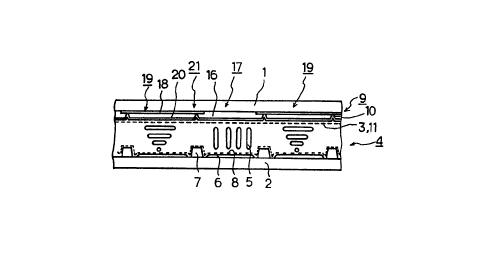
Then, as shown in Figure 6, for the pixels 13, 15 and
17 at which the red, green and blue filters 12, 14 and
16 should be formed, Cr is removed by photolithography
from locations which are slightly (2 - 5 ~m) inside the
locations corresponding to the pixel electrQdRs 6.farmed
on the glass substrate 2. At this time, Cr i8 not removed
from the pixels 19 at which the translucent filters 18
are to be formed.
In addition, for the pixels at which the red, green and
blue filters 12, 14 and 16 should be formed, color filters
. .
JA9-87-006
12~33473
of corresponding colors are formed on the glass substrate
1 and residual Cr as the red, green and blue filters
12, 14 and 16 by, for example, a gelatin dyeing method.
On the other hand, for the pixels 19 at which the trans-
lucent filters 18 should be formed, gelatin without
dyeing process is formed on Cr as the transparent material
20.
Then, the protective layer 10 and the common electrodes
11 are laminated.
In the manufacturing method as described above, the
step for forming the light shielding layer 21 can be
performed simultaneously with the step for forming other
filters so that the number of steps can be reduced.
Although, i~ th~ embodiment described above, the light
shielding layer 21 is constituted by laminating Cr and
the filters 12, 14 and 16 of corresponding colors respec-
tively, it may be arranged so that, for example, as
shown in Figure 7, the light shielding layer 21 is con-
stituted by laminating Cr and the filters of all colors,
18
. JA9-87-006
12~3473
for example, in this case, by laminating Cr and red
filter 12, and green filter 14, and blue filter 16. In
this case, the optical density O.D. of the light shield-
ing layer 21 becomes 3.65, which provides higher con-
trast. In addition, only one photomask is needed in
manufacturing. Furthermore, the variation of the thick-
ness of the shielding layer 21 becomes small.
In the above embodiments Cr is used as the translucent
filter 18, other metal such as Mo, Ti, Ta, or Ni may be
used instead of Cr.
It is desirable for the thickness of the translucent
filter 18 to be sufficiently less than that of the
filters 12, 14 and 16, in view of the difference of the
level when the peripheri~s of. the.filters l~, 14 and 16
overlap with the trans~ucent filter.18.
Although the above embodiment provides the filters on
the side of the common electrodes, it may be possible
to provide the filters on the side of the pixel elec- !
trodes.
19
JA9-87-006
~2834~3
Although one display unit is of a square consisting of
squares of four colors in the above embodiments, the
invention does not restrict its shape or its number.
For example, one display unit may consist of two
pixels, each pixel may be a rectangular, or a pixel
pitch may be shifted by one half.
As described, according to the color liquid crystal
display of the invention, a multicolor display can be
attained by combination with the translucent filter,
high contrast can be obtained by the light shielding
layer in which the color filters are laminated on the
translucent filter, and the light shielding layer can
be made thinner. In addition, according to the manu-
facturing method of the invention, a color liquid
crystal display that can display multiple colorsrin
such high contract can be efficiently manufactured.