Note: Descriptions are shown in the official language in which they were submitted.
01 - 1 -
02 BACKGROUND OF THE INVENTION
03 (Field of Technology)
04 The present invention relates to a tracking system
05 for an optical memory device of a type wherein any of the
06 information recording, reproduction and erasing can be
07 carried out by radiating a laser beam to a memory
08 medium.
09 BRIEF DESCRIPTION OF THE DRAWINGS
Features of the present invention will become clear
11 from the following description taken in conjunction with
12 preferred embodiments thereof with reference to the
13 accompanying drawings, in which:
14 Fig. 1 is a schematic diagram showing an optical
15 head for magneto optic disc according to one embodiment
16 of the present invention;
17 Fig. 2 is a diagram showing an electric circuit
18 forming a detecting means for detecting a tracking error
19 signal;
Fig. 3 is a circuit block diagram showing the
21 circuit of the detecting means;
22 Fig. 4 is a chart showing waveforms of signals
23 appearing in the circuit of Fig. 3;
24 Fig. 5 is a schematic diagram showing an optical
25 head for an optical disc to which a tracking system is
26 applied according to a second embodiment of the present
27 invention;
28 Fig. 6 is a schematic diagram showing a
29 relationship between the respective positions of laser
~,~
01 - la -
02 beam spots incident on the optical disc, the arrangement
03 of detecting elements of a photo-detector and the
04 respective positions of the laser beam spots reflected
05 upon the detecting elements;
06 Fig. 7 is a circuit block diagram showing a circuit
07 used to effect a processing necessary to produce a
08 feedback control signal;
09 Figs. 8a and 8b are charts showing waveforms of
signals;
11 Fig. 9 is a diagram similar to Fig. 7 showing a
12 modified form of the circuit;
13 Figs. 10(a), 10(b) and 10(c) are charts showing
14 waveforms of signals;
Fig. 11 is a perspective view of a portion of a
16 disc substrate;
17 Figs. 12(a), 12(b) and 12(c) are plan views of a
18 portion of the disc substrate onto which the laser beams
19 are projected;
Fig. 13(a) is a plan view of a portion of the disc
21 substrate onto which the laser beams are projected;
22 Fig. 13(b) is a schematic diagram showing the
23 detector on which the beam spot is reflected; and
24 Fig. 13(c) is a diagram showing waveforms of the
signals.
26 (Description of the Prior Art)
27 Optical memory devices have recently drawn the
28 attention of people as a high density, high capacity
29 memory device. ~he reason for this optical memory device
4~
01 - lb -
02 to be of high density and high capacity is because the
03 size of each bit which represents the~unit of information
04 storage capacity can be reduced to a diameter of about
05 1 ~m. ~his, in turn, however, imposes some limitations
06 on the optical memory device. More specifically, in
07 order for information to be recorded on, or reproduced ~-
08 from, a predetermined locationj the light beam is
09 required to be accurately positioned.
Because of the foregoing, when using a disc capable
11 of accommodating information additionally recorded on a
12 disc capable of recording information simultaneously with
13 erasure of the previously recorded information, it is a
14 general practice for the disc substrate to be permanently
provided with beam guide tracks or address information.
16 The guide tracks generally have a shape as shown
17 in Fig. 11 of the accompanying drawinge nd are in the form
~ .
' .
~ j .
. .
.~3
.
~4~
- 2 -
of grooves of a depth generally equal to the wavelength A
divided by the product of the refractive index n times 8,
i.e., ~/8n. Any of the information recording, reproduction
S and erasing is carried out while the light beam undergoes
scanning guided along these guide grooves.
As a means for sensing a tracking signal from the
guide grooves, two methods are well known; a Twin Spot method
(a three-beam method) such as generally used in association
with VD (video disc) and CD (compact disc), and a push-pull
method such as generally used in association with an optically
writeable disc. The Twin Spot method and the push-pull method
are illustrated respectively in Figs. 12 and 13 of the
accompanying drawings.
IS The Twin Spot method has an advantage in that a
stable tracking performance can be achieved even though a pick
up is inclined relative to the optical disc substrate.
However, it has a problem in that, when a tracking beam scans
a boundary between a guide groove region G and an address
information region A constituted by a plurality of pits as
shown in Fig. 12(a), the tracking tends to be disturbed
because of the difference between a diffraction efficiency on
the leading beam Bl and that on the trailing beam B2. It is
to be noted that reference character R used in Fig. 12(b)
represents recorded bits.
On the other hand, although the push-pull method
is generally free from the above-mentioned problem inherent
. . . , ,... .. ,., . . . ,:
. . .
4~
in the Twin Spot method because of the tracking performed by a
single beam B4 as shown in Fig. 13(a), it has a problem in
that, because the position of the light beam which has been
S reflected towards a detector D shown in Fig. 13(b) tends to
displace relative thereto in the event of occurrence of a
shift in position of a lens as a result of the tracking or in
the event of inclination of the pick-up relative to the disc,
the tracking error signal tends to accompany a steady drift
lo which will bring about a steady shift in tracking.
Accordingly, in the event that the pick-up has inclined
relative to the disc, the pattern of diffraction occurring at
the guide groove region and that at the address information
region differ from each other and, as a result thereof, the
amount of tracking shift necessarily deviates to such an
extent as to result in the disturbed tracking at the boundary.
Figs. 12(a) to 12(c) and Figs. 13(a) to 13(c) are schematic
representations illustrative of the change in tracking error
signal occurring during the tracking at the boundary according
to these two methods, respectively.
In these figures, the servo region is considered to
be sufficiently lower than the pit reproducing frequency and,
therefore, an output of the detector during the tracking at
the address information region is shown as an average value.
Fig. 12 applies where the difference in amount of beams
reflected is taken as the tracking error signal, whereas
Fig. 13 applies where the difference in output from
2~'
- - ~ . ...
,
~ lX~4~2~
detectors for detecting two split beam components is taken as
the tracking error signal.
SUMMARY OF THE INVENTION
S Accordingly, the present invention has been devised
to substantially eliminating the above described problems and
has for its essential object to provide a tracking system
wherein a relatively easy signal processing means is employed
to enable the tracking to be performed in a stabilized manner,
even to discontinuous guide grooves, with no need to take
special measures for any disc substrate.
In accordance with an embodiment of the invention, a
tracking system for an optical memory disc having a plurality
of recording tracks thereon including track address regions
and track information regions is comprised of an optical head
assembly including light beam producing apparatus for
producing a main light beam and two auxiliary light beams, the
main and auxiliary beams being scanned over the plurality of
; tracks, detecting apparatus for detecting light beams
reflected from the tracks as a result of the scanning and
~ producing a first tracking error signal in response to the
; light reflected from the main beam and a second tracking error
signal in response to the light reflected from the two
auxiliary beams, and tracking control apparatus for performing
tracking control of the main beam on one of the tracks in
response to said first tracking error signal at a boundary
between a track address region and a track information region,
and the second tracking error signal at track regions other
than the boundary.
' ~
, ' .
.
1~4;~
DETAILED DESCRIPTION OF THE EMBODIMENTS
Figs. 1 and 2 illustrate the structure of an optical
head for magneto optic disc and a circuit forming a detecting
means for detecting a tracking error signal outputted form the
optical head, respectively.
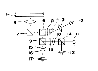
Referring first to Fig. 1, reference number
represents a magneto optic disc comprising a disc substrate
which has the previously discussed guide grooves and address
information and is coated with a magnetizeable layer having an
anisotropy of magnetism in a vertical direction. A laser beam
produced from a semiconductor laser device 2 travels through a
collimator lens 3 and then through a shaping prism 4 by which
the cross-sectional representation of the laser beams which is
elliptical is transformed into a generally circular shape.
Reference number 5 represents a diffraction grating for
splitting the laser beam by the utilization of a diffraction
effect, the diffracted light of a spectral degree of O and +l
being utilized. A polarizing beam splitter 6 is disposed
between the diffraction grating 5 and an objective lens 8 for
projecting a tiny spot of laser beam onto the
magnetizeable layer on the magneto optic disc after having
been deflected 90 by a total reflecting mirror 7. This
polarizing beam splitter 6 serves to improve the
polarization ratio of the incoming light and to further
rotate the plane of polarization of the light, reflected
from the disc, for generally increasing the angle of magneto
4~
6 _
optic rotation. This beam splitter 6 also serves to guide a
portion of the laser beam toward photo-detectors 11, 12 and
17 as will be described later.
The objective lens 8 referred to above is in
practice driven by a servo control circuit (not shown) so
that the size and position of the light spot projected onto
the information tracks on the magnetizeable layer of the
disc can be adjusted. Reference numeral 9 represents a
polarizing beam splitter having, as is the case with the
beam splitter 6, a function of increasing the angle of
magneto optic rotation with respect to the reflected light.
Reference numeral 10 represents a spot lens for projecting
the information light, reflected from the beam splitter 9,
onto the photo-detectors 11 and 12 in a predetermined spot
size. A half wavelength plate 13 is positioned between the
beam splitter 9 and the spot lens 10 for rotating the plane
of the polarization of the information light in a direction
intermediate between S-axis and P-axis of a polarizing beam
splitter 14 which acts as an analyzer. Reference numeral 15
represents a spot lens, and reference numeral 16 represents
a cylindrical lens so disposed as to have its focal line
inclined 45 relative to the direction of connection of the
guide grooves of the magneto optic disc 1.
Positioned on one side of the cylindrical lens 16
opposite to the spot lens 15 is the photo-detector of
composite element type which includes six photo-detector
~ 4~
-- 7
elements A to F that are arranged in a pattern as shown in
- Fig. 2. By the cumulative effects of the spot lens 15 and
the cylindrical lens 16, both the change in relative dis-
tance between the magneiizeable layer of the magneto optic
disc 1 and the objective lens 8, and the deviation in a
position between a condition of, the light spot on the
magnetizeable layer and the information track (guide
grooves) can be detected. A method of detecting these servo
signals is similar to that used in any one of the astigma
tism method, the three-beam method and the push~pull method,
all generally used in association with the optical disc.
Fig. 2 illustrates the relationship in position
between the photo-detector 17 of composite element type and
the reflected information light from the magneto optic disc
1, and also a detecting means. Based on respective outputs
SA, SB, SC and SD of four light receiving elements A, B, C
and D positioned centrally of the detecting means 17, a
focusing error signal FE and a main beam tracking error
j signal TEo can be obtained from the following equations.
FE = (SA + SC) - (SB + SD)
TEo = (SA + SD) - (SC + SB)
~ Also, based on respective outputs of light receiv-
; ing elements E and F positioned on respective sides of the
four light receiving elements A, B, C and D, a tracking
error signal TEl resulting from two auxiliary beams can be
,1l obtained from the following equation.
:
4~2
.~
8 --
TEl = SF - SE
-~ Of these error signals, the focusing error signal
FE is used to control the drive of the objective lens 8 in a
direction parallel to the optical axis which is effected by
the servo control circuit and a drive device.
On the other hand, the main beam tracking error
signal TEo and the tracking error slgnals TE1 resulting from
the two auxiliary beams are, after having been processed by
some processes as will be described later, used to control
the drive of the object lens 8 in a direction transverse to
the track which is effected by the servo control circuit and
the drive device.
Hereinafter, the processes necessary to effect the
tracking by the use of the above-mentioned two tracking
error signals will be described.
Fiy. 3 is a circuit block diagram used to explain
the first process. Reference numeral 18 represents a low
pass filter unit for obtaining a low frequency component of
the main beam tracking error signal TEo~ The low frequency
component filtered through the low pass filter unit 18 is
fed to a sample~and-hold circuit 19 for sampllng and holding
- the oùtput from the filter unit 18 in synchronism with a
timing signal as will be described later. Reference numeral
represents a differential circuit for outputting
difference signal indicative of the difference between the
output from the sample-and-hold circuit 19 and the maim beam
B
4;~X
tracking error signal TEo~ said difference signal being in
turn fed to a switching circuit 21 which is operable to effect
a switching between the tracking error signal TE1 and the
S tracking error signal processed as described above (i.e.,
output from the differential circuit 20) in synchronism with
the timing signal. The switching operation of the switching
circuit 21 is performed by the utilization of the timing
signal, the waveform of which is shown by (a) in Fig. 4, in
such a way that, at regions other than the address regions and
the boundary regions, the tracking can be carried out
according to the Twin Spot method (i.e., the signal TEI)
wherein the stable tracking error signal can be obtained, but
at the address regions and the boundary regions, the amount of
offset of the main beam tracking error signal TEo can be
monitored during the tracking according to the Twin Spot
method and the tracking can be carried out according to the
push-pull method (i.e., the output of the differential circuit
20) by the main beam with this taken as a target value. Also,
by the utilization of the timing signal shown by (b) in Fig.
4, the push-pull method (i.e., the output of the differential
circuit 20) can be utilized for the tracking only at the
boundary regions where the error signal (i.e., the signal TEl)
tends to be disturbed according to the Twin Spot method.
As the second process which can bring about a
similar effect, a method can be contemplated wherein either
.
~ 4~
-- 10 --
the error signal associated with the auxiliary beams or the
main beam tracking error signal is monitored while the
tracking is normally carried out according to the Twin Spot
method, but the tracking at the address regions and the
boundary regions is carried out by holding the tracking error
signal TE1 accordir.g to the Twin Spot method or a low pass
filter output signal of the push-pull signal TEo associated
with the main beam. This process can work very well where the
time required to pass the address regions is short and the
amount of movement of tracks during this time is also small.
Although not discussed, care must be taken that the
sensitivity of detection of various tracking errGr signals
must be optically or electrically consistent and that any
change in output incident to change in power of the laser
during the recording and the erasure must be controlled by any
suitable method, for example, by the use of an automatic gain
;1 control circuit.
The tracking system according to the foregoing
; 20 embodiment is advantageous in that, since the advantage of the
Twin Spot method is utilized, the stable tracking can take
place even with the optical disc having the address
information partially preformatted.
The tracking system according to a different
embodiment of the present invention will now be described with
paeticular reference to Figs. 5 to 8.
.~
,
~,~
.
.
~ 4~2
In Fig. 5, which illustrates the construction of an
optical head for use with an optical disc to which the present
invention has been applied, reference numeral loO represents
; S the optical disc having permanently formed therein non-
continued guide grooves representative of the previously
- discussed guide grooves and address information. Reference
numeral 102 represents a laser device for producing a
predetermined laser beam. Reference numeral 103 represents a
diffraction grating for producing a main beam used to carry
out the recording, reproduction or erasing, as well as
auxiliary beams used to obtain auxiliary tracking error
signals, said grating having a direction of diffraction
I
located on respective sides of a recording track. Reference
~, 15 numeral 104 represents a beam splitter operable to pass a
s portion of the incoming laser beam therethrough and also to
,l guide the laser beam, which has been reflected from the
,,;,
optical disc 100, towards a photo-detector 108. The portion
of the laser beam which has passed through the beam splitter
20 104 is formed by an objective lens 105 into a tiny spot of
~$ light which is projected onto the optical disc 100. This
objective lens 105 can be controlled by a servo control
circuit and a lens drive circuit, both not shown, so as to be
moved in a direction parallel to the optical axis and also in
25 a direction perpendicular to the tracks. In this way, the
size and the position of the spot of the laser light projected
onto the optical disc 100 can be adjusted.
X
~:
.,
1~4~
- 12 -
The laser beam which has been reflected from the
optical disc 100 and then guided by the beam splitter 104
travels towards the photo-detector 108 of composite element
i 5 type through a spot lens 106 and then through a cylindrical
lens 107 so positioned as to have its focal line inclined 45
relative to the direction of connection of the guide grooves
of the optical disc 100. The relationship between the
position of the spot of the laser beam projected onto the
optical disc 1, the arrangement of detecting elements A to F
of the photo-detector 8, and the position of the spot of the
reflected light on each detecting element is shown in Fig. 6.
Referring to Fig. 6, reference numeral 100'
represents a recording track formed on the optical disc 1,
s IS reference character a represents the spot of the main beam of
thc incident laser projected on the recording track 100', and
reference characters b and c represent respective spots of the
auxiliary beams. Reference character a' represents a spot
~, ~
formed by a reflected light of the main beam, whereas
reference characters b' and c' represent respective spots
:
formed by reflected light of the auxiliary beams. In the
construction shown therein, a focusing error signal FE
necessary to move the objective lens 105 in the direction
parallel to the optical axis, and tracking error signals TEo
~; ~ ~ and TEl necessary to move the objective lens 105 in the
.s
~ direction perpendicular to the tracks can be obtained
.i~: :
~: '
'
'' ' ~ '
,
'
~4~2~
- 13 -
- according to the astigmatism system, the push~pull system
- and the three-beam system, respectively, and ca~ be deter-
mined by performing calculation according to the following
equations.
FE = (SA +SC) - (SB + SD)
TEo = (SA +SD) - (SC + SB)
. TEl = SF -- SE
wherein SA, SB, SC, SD, SE and SF represent detection
signals outputted from the detecting elements, respeGtively.
Fig. 7 illustrates a circuit block diagram showing
a processing circuit for producing a feedback control signal
on the basis of the tracking error signals TEo and TEl
referred to above. Reference numeral 109 represents a low
; pass filter for extracting only a low frequency component of
; 15 the tracking error signal TEl according to the Twin Spot
method, and reference numeral 110 represents a differential
circuit for performing addition or subtraction between the
output of the low pass filter 109 and the tracking error
signal TEo according to the push-pull system. Whether the
differential circuit 110 performs addition or whether it
performs subtraction depends on the relationship in phase
~' between the error signals TE1 and TEo~ By way of example,
when the error signal TEo according to the push-pull system
matches in phase with the error signal TE1 according to the
Twin Spot system as shown in Fig. 8 at the time an offset
occurs in the spot of the incident laser beam, an offset
, , .
4i~
- 14 -
occurring in the error signal TEo can be compensated for by
adding the low frequency component, indicated by ~ in Fig.
8(b), of the error signal TE1 produced incident to the
s tracking to the error signal TE0, and therefore, the accurate
tracking can be achieved as can be understood from Fig. 8(b).
An output from the calculator 110 is fed to a
- switching circuit provided for enabling a stabilized
withdrawal of the tracking, which circuit 111 can perform such
a switching operation that the tracking error signal TEl
according to the Twin Spot system can be utilized in the event
that no steady offset occur in the error signal at the time of
withdrawal from the track, but the tracking error signal which
has been processed in the manner as hereinabove described can
be utilized subsequent to the withdrawal.
The processing circuit described with reference to
and shown in Fig. 7 can be modified as shown in Fig. 9 wherein
like parts shown in Fig. 9 are designated by like reference
numerals used in Fig. 7. Reference numerals 112 and 113
represent calculators, respectively, each of said calculators
being similar to the calculator 110 shown in Fig. 7. This
circuit shown in Fig. 9 is so designed that, where the error
signal TEo according to the push-pull system and the error
signal TEl according to the Twin Spot system can be obtained
from a combination of the calculator 112 and the calculator
109 as shown in Fig. lO(b), a difference signal S
',
:
1~4~
- 15 -
representative of the difference between the signal S' and the
error signal TEo can be obtained from the calculator 113 as
shown in Fig. lO(c). By the utilization of this difference
S signal s, the accurate tracking can be accomplished.
Thus, by the use of the foregoing technique
according to the present invention, a tracking error signal
; for the tracking can be automatically corrected even though
the offset occurs in the push-pull signal, and therefore, the
stable tracking can be accomplished. In addition, since the
reduced component of the tracking error signal according to
the Twin Spot system is utilized, any external disturbance
which would occur during the tracking at the boundary between
the recorded nor non-recorded area or the guide grooves and
; 15 address region can be minimized to a negligible extent.
From the foregoing, it is clear that the present
invention is effective to provide the tracking system which
utilizes the advantages of both the Twin Spot system and the
push-pull system. Moreover, even with the optical disc having
the guide grooves and the address regions as well as the
optical disc of a type which would result in change of the
reflectivity, the tracking system of the present invention can
ensure a sufficiently stabilized tracking performance.
4~
_ 16 _
. Although the present invention has been fully
described by way of example with reference to the accompany-
ing drawings, it is to be noted here that various changes
and modifications are apparent to those skilled in the art.
Such changes and modifications are to be understood as
included within the scope of. the present invention, unless
: they depart therefrom.
"
.
: .;
,
,,
,~ ~q
'~
.~, ~' ' ,
i ~ :
, .
~'
.
.
~ - ~
,.
.,: .
~ ' .; ' . , ,: '