Note: Descriptions are shown in the official language in which they were submitted.
~2~7~36
ELECTROSTP.TIC DISC~IARGE PROTECTION
FOPc A PRINTED CIRC~JIT BOARD
Field of the Invention
The present invention relates generally to
electrostatic discharge protection o~ electronic circuits.
More speci~ically, the present invention relates to
electrostatic discharge protection for a print~d circuit
bsard .
Back~round of the Invention
In general, products containing printed circuit
board ~PCB) assemblies must be protected from electrostatic
discharge (ESD), which results, in some cases, from a userls
natural electrostatic charge build up and consequ~nt
discharge with touching of the product housing near an
opPning. Electrostatic discharge protection is necessary to
prevent, or to reduce, damage to the sensitive components on
the PCB assembly. Damage resulting from an electrostatic
discharge may range from a brief intermittent fault to a
catastrophic fault wherein the circuit is no longer capable
of functioning. Standard~ have been set by cha International
EleckrotQchnical Commission to ensure proper protection
against electrostatic discharge within electronic components.
one such standard requires that talephone sets be made to
withstand an eleatrostatic discharge of 15,000 volts.
Typically this high-energy ESD is capable of destroying
solid-state components in the telephone set.
Many methods of preventing electrostatic discharge
from occurring exist in the prior art. One method is to
position the telephone set's PCB perimeter ~ar enough in from
the walls of the plastic housing of the telephone set so that
a 15,000 volt electro~tatic discharge at the plastic housing
~annot jump from the plastic housing to the printed circuit
~5 board. Positioning a PCB in such a manner creates an air gap
which by virtue of its length prevents an electrostatic
discharge from arcing, up to a given k~lovolt level dependent
on the size of th~ air gap. However, positionlng a PCB in
d~
~9~21~
such a mann~r is not always possible as an objective in
telephone design is to make the set as physically small as
possible so that it takes up a minimum amount of space on a
desk or table, and so that it is aesthetically pleasing.
Another method is to increase the ESD jump
distance, and hence the ~SD voltage maximum, by having an
internal plastic barricade molded as part of the plastic
housing. This forces any ESD to arc a greater distancs than
it otherwise would and khus prevents an axc from initiating
at a given voltage level.
A further method is to put an insulated cover or
sleeving over the region of concern which effectively
increases the available arc jump distance.
Yet another method is to suspend, or otherwise
locate, a wire, soldered to the electrostatic ground at one
end, from the PC~ much like a lightening arrestor so that it
will attract ESD at a particularly sensitlve location to
prevent it from gettiny further into the circuitry.
While all of the abova methods are effective, they
each can add to the complexity of the design of the telephone
~et or necessitate that the telephone set be made larger to
accommodate the electrostatic discharge protection.
Information regarding the state of the prior art
may be found in the following references- United States
Patent 4,821,320 issued April 11, 1989 in the name o T.J.
Andert et al.; United States Patent 4,667,266 issued May 19,
1987 in the name of Masuo]ca et al.; United States Patent
4,532,419 i~sued July 30, 1985 in the name of M. Takeda; and
United States Patent 4,531,176 issued July 23, 1985 in the
name of R.L~ Beecher.
Summary of the Invention
~ he present invention provides a simple,
effective, and inexpensive way of preventing electrostatic
discharge from entering further into the circuitry while not
increasing the size or complexity of a surrounding housing.
The present in~ntion uses a PCB conductor path, connected to
a source of reference potential, which is placed near the
~9'7~
perimeter of the PCB adjacent to a probable housing mating
edge breakdown region or at a region of the PCB near an
opening in the housing, as for example where a button or
the like may protrude. By so placing such a conductor
path, the electrostatic discharge tends to jump to this
path. To prevent the possibility of the ESD jumping past
the perimeter conductor path, the conductor path is
designed so as to have pointed, or nearly pointed,
protrusions extending from the path at intermittent
locations. The protrusions act like lighting rods by using
the principle that an electrostatic discharge is more
likely to jump to sharp objects than to smooth objects. In
other words, the protrusions attract the ESD, thereby
preventing the ESD from striking elsewhere on the PCB.
Stated in other terms the present invention is a
method of reducing electrostatic discharge damage to a
printed circuit board, the method comprising the steps of:
providing at least one conductor path connected to a source
of reference potential, the at least one conductor path
placed alony at least one portion of at least one edge of
the printed circuit board; and, providing a plurality of
approximately pointed protrusions along the length of the
at least one conductor path, each of said protrusions being
an integral part oE said at least one conductor path and
having a base approximately equal to the width of said at
least one conductor path and an apex approximately half of
the width of said at least one conductor path from said
base; wherein each of said plurality of approximately
pointed protrusions has its apex near said at least one
edge of said printed circuit board and wherein each of said
plurality of approximately pointed protrusi.ons is nearer to
said at least one edge than any other conductor on said
p-rinted circuit board.
Stated in yet other terms the present invention
is a printed circuit board, the printed circuit board being
formed from a dielectric substrate and having thereon a
plurality of conductor paths for interconnecting electrical
72~6
components thereon, the printed circuit board comprising:
at least one conductor path for connection to a source of
reference potential, for providing protection against
electrostatic discharge,the at least one conductor path
placed along at least one portion of at least one edge of
the printed circuit board; the at least one conductor path
having formed therewith a plurality of approximately
pointed protrusions along the length of the at least one
conductor path, each of said protrusions being an integral
part of said at least one conductor path and having a base
approximately equal to the width of said at least one
conductor path and an apex approximately half of the width
of said at least one conductor path from said base; wherein
each of said plurality of approximately pointed protrusions
has its apex near said at least one edge of said printed
circuit board and wherein each of said plurality of
approximately pointed protrusions is nearer to said at
least one edge than any other conductor on said printed
:. 3a
~29~ 6
Brief Description o~ the Drawings
The invention will be readily understood by the
following description o~ a preferred embodiment, by way of
example, in conjunction with the accompanying diagrammatic
drawings, in which:
Figure 1 is a top plan view of a printed circuit
board incorporating the present invention:
Figure 2 is a partial top plan view of an
electrostatic discharge conductor path according to the
present invention.
Detailed Description o~ the Invention
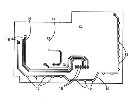
Figure 1 illustrates a printed circuit board 20
having a plurality of conductor paths 14. Conductor paths 14
]5 are provided to interconnect electrical circuitry (not shown)
affixed to the PCB 20 via lands 16. According to the present
invention, placed along a portion of the perimeter of the PCB
20 is an electrostatic discharge conductor path 10 which is
connected to a source of reference potential ~not shown).
The conduator path 10 is placed along the perimeter of the
RCB 20 so as to aat as a direct path for any electrostatic
discharge which may occur around the parting line of a
plastic housing encasing the PCB 20. The conductor path 10
is not covered or coated with insulating solder resist
thereby facilitating a conductive path for an electrostatic
discharge. In practice, the conduator path 10 need only be
placed along the edge, or edges, of the PCB 20 nearest the
region o~ the plastic housing that will result in an
electrostatic discharg~ breakdown, thereby reducing the area
needed to accommodate the conduator path 10 and consequently
leaving more room for other conductor paths 14 on the PCB
20.
To ensure that an electrostatic discharge will not
jump over the conductor path 10, pointed, or nearly pointed,
protrusions 12 (further illustrated in Figure 2) are plaeed
along the length of the conductor path 10. ~he apexes of the
protrusions 12 are placed towards the edge or edges of the
PCB 20 and extend beyond any other conductor paths 14 or
~g7~
lands 16 that may appear on the edges of the PCB 20. The
protrusions 12 pxovide a sharp edge which attracts an
electrostatic discharge onto conductor path 10.
It can be noted that the protrusions 12 may b~
regularly or irregularly spaced along the length of conductor
path 10. The determination as to the location of the
protrusions 12 will depend on the amount of protection
reguired at a particular location on PCB 20.
The protrusions need not be specifically shaped as
shown in the Figures; they could be rectangular protrusions,
or regular and/or irragular pointed configurations
protruding along the length of the at least one conductor
path. The distinguishing ~eature o~ the protrusion is its
sharp or nearly-sharp points pref~rably pointing towards the
direction from which the ESD might enter the PCB, as for
example through the mating edges of the housing pieces. The
size of the protrusions are in general controlled by the
amount of available space on the PCB and the acceptable
closeness of them to the ESD entry regions.
In a preferred em~odiment, the width of the
conductor path 10 is approximately 0.02 inches. Each o~ the
protrusions 12 has a base of approximately 0.02 inches and an
apex approximately 0.01 inches from the conductor path 10.
The present invention provides a simple yet
relatively effective method o~ reducing electrostatic
discharge damage to components on a printed circuit board.
Numerous other modifications, variations, and
adaptations may be made to the particular embodiments of the
invention described above without departing from the scope of
the claims.