Note: Descriptions are shown in the official language in which they were submitted.
l~g8367
BACKGROUND OF THE INVENTION
I. Field of the Invention
The present invention relates to an electrical connector
assembly for termination of coaxial cable enabling rapid
attachment to and detachment from a PCB of a large number of
signal leads while ensuring an acceptable level of controlled
impedance from the coaxial cable to the PCB.
II. Description of the Prior Art
Requirements of backplane interconnection for electronic data
processi-ng and telecommunications applications require over
increasing densities of electrical leads to accommodate an
ever larger number of signals within a given unit of space.
At the same time, the space requirements are ever decreasing
and this combination has the undesirable effect of increasing
noise potential by reason of the increased density of the
signal leads. At the same time, it is necessary to maintain
a matched impedance from the signal wire, through the region
of the interconnection, and into the printed circuit board
(PCB) with which the signal leads are being terminated.
Typical of the problem being faced, and solved, by the
present invention i6 the ability to achieve a standard 50 ohm
--1--
129~3~7 04805-9 GWH:jy
impedance level for a defined density of leads for which it
was only previously possible to obtain a 37 ohm impedance for
a lead density which was less dense by approximately 25
percent. All known existing small diameter coaxial contacts
(for example, contacts having a diameter of 0.100 inches) use
insulation material for the dielectric. This results in lower
impedance value. In contrast, the present invention employs
air as the dielectric thereby achieving a higher impedance in
a smaller space.
S~MMARY OF TH E I NVENT I ON
The present connector assembly was conceived and has now been
reduced to practice to satisfy the more stringent connection
requirements referred to above. Thus, a controlled impedance
connector assembly is disclosed which includes a receptacle
adapted for mounting on a printed circuit board (PCB) and for
mating reception of a plug which carries terminal ends of a
plurality of coaxial contacts. A honeycomb grounding block is
mounted in the plug to engageably receive the outer conductor
of each coaxial contact, the inner conductor of each coaxial
contact being electrically coupled to a signal lead by a first
contact member. Signal pin contacts within the receptacle and
electrically coupled with the signal conductors of the PCB are
electrically coupled with each inner sleeve of the coaxial
contact when the plug is inserted into the receptacle.
~,
129~367 04805-9 GWH:jy
Likewise, ground pin contacts within the receptacle and
electrically coupled with the ground conductors of the PCB
have second and third spaced resilient contact members,
respectively, engaging the grounding block at distances
farther from and nearer to the PCB than the first contact
members. Within each coaxial contact, air is a primary
dielectric between the two is controlled to thereby maintain a
substantially uniform impedance in the region of the connector
matched to that of the coaxial cable and the PCB. The signal
and ground pin contacts may be pre-assembled in a holding
block for storage or shipping enabling ready assembly into the
receptacle and easy insertion of a plurality of small pins
into small holes in the PCB, simultaneously, by aligning the
tips of the pins through funnel shaped holes in the
receptacle. Alignment of the holes in the receptacles with
those in the PCB is accomplished by means of positioning pegs
molded in the receptacle. Thereafter, connection to the PCB
is accomplished at the time the connector assembly is being
installed. The plug is of a sturdy clam shell design, and
reusable zipper-type tubing is used as a jacket to
protectively enclose the coaxial cable in a bundle as they
extend away from the plug.
In a typical application, the present connector assembly
enables termination of seventy two coaxial cables in a defined
area of three quarters inch by one and one half inches with
12~8367 04805-9 GWH:jy
0.120 spacing between centers of adjoining contacts. By
reason of the unique design of the invention, as a connection
is made by the plug with its associated receptacle, the
coaxial shield associated with each signal lead is placed at
ground potential prior to electrical coupling of the signal
lead. Additionally, when the plug is withdrawn or
disconnected, from the receptacle, the coaxial shield remains
grounded until after its associated signal pin has been
disconnected from the circuit. This arrangement provides for
electromagnetic shielding for each of the signal wires and
thereby assures a low noise level in the circuit.
Furthermore, when the plug is fully inserted into its mating
receptacle, the signal is protected from outside interferences
up to within 0.100 nches of the PCB. The signal is
surrounded by four ground posts as it passes through that
0.100 inch distance which serve to provide a continuins
shielding of the signal.
The present connector assembly also eases the ability to
assemble multiple leads in a cramped location. For example,
in the typical assembly referred to above enabling termination
of seventy two coaxial cables in a defined area of three
quarters inch by one and one half inches, tails of 122 contact
pins must be mounted in a receptacle so as to be aligned with
a similar number of holes in the mating PCB for subsequent
,~
1298367 04805-9 GWH:jy
termination. Again, typically, the holes in the PCB have
diameters generally in the range of 0.015 to 0.022 inches and
the width of the tails is generally less than 0.22 inches.
Notwithstanding these very small dimensions, the invention
enables rapid and accurate assembly of the contact pins in the
receptacle.
Another benefit of the present assembly resides in an improved
solderless, one step, crimping operation by means of which
each coaxial contact is terminated on an end of a coaxial
cable lead. Specifically, the present assembly provides for
crimping of the inner sleeve through openings in the outer
sleeve of the contact while simultaneously crimping the outer
sleeve.
Other and further feature, objects, advantages, and benefits
of the present assembly will become apparent in the following
description taken in conjunction with the following drawings.
It is to be understood that the foregoing general description
and the following detailed description are exemplary and
explanatory but are not to be restrictive of the invention.
The accompanying drawings, which are incorporated herein and
constitute a part of this invention, illustrate one of the
embodiments of the invention and, together with the
description, serve to explain the principles of the invention
in general terms. Like numerals refer to like parts
throughout the disclosure.
- 5 -
12~8367
BRIEF DESCRIPTION OF THE DRAWINGS
Fig. 1 is a partially exploded perspective view illustrating
a controlled impedance connector assembly embodying the
invention;
Fig. 2 is a further exploded perspective view of components
illustrated in Fig. 1;
Fig. 2A is a detail partial top plan view, of a honeycomb
grounding block utilized by the invention;
Fig. 3 is an exploded elevation view, certain parts being cut
away and shown ~n section, to illustrate the plug utilized by
the invention;
Fig. 4 is a top plan view of one of the components
illustrated in Fig. 2;
Fig. 5 is a cross section view taken generally along line
5--5 in Fig. 4 but including additional components not
illustrated in Fig. 4;
Fig. 6 is a detail elevation view, partly cut away and in
section, illustrating the relationship between various
components of the invention which would result in providing a
maximum eletromagnetic shielding for the signal wires of the
connector assembly of the invention;
--6--
12~1~367
Fig. 7 is a perspective view of a signal pin contact utilized
with the invention;
Fig. 8 is a perspective view of a ground pin contact utilized
with the invention;
Fig. 9 is an elevation view, partly cut away and in section,
illustrating the manner of assembling and mounting pin
contacts to the receptacle and to the PCB illustrated in Fig.
1 and illustrating, respectively, initial and final positions
of the pin contacts during the assembly procedure;
Fig. 10 is a detail perspective view of a bundle of leads
typically used with the invention and provided with a
removable outer protective covering; and
Fig. 11 is a detail elevation view in section illustrating in
enlarged form a part of the construction illustrated in Fig.
5;
Fig. 12 is a side elevation view, partly cut away and in
section, illustrating a coaxial terminal mounted on a coaxial
cable lead;
Fig. 12A is an end elevation view of the coaxial terminal
illustrated in Fig. 12, a part having been eliminated for
clarity;
Fig. 12B is a side elevation view, similar to Fig. 12 with
the coaxial terminal lead rotated 90 about its longitudinal
--7--
12~8367
axis from the position illustrated in Fig. 12;
Fig. 13 is an exploded perspective view illustrating a PCB
mounted receptacle with a pair of holding blocks positioned
for mating reception therewith;
Fig. 14 is a top plan view of a receptacle of the invention
with one holding bloclc in mating reception therewith;
Fig. 15 is a cross section view taken generally along line
15--15 of Fig. 14 but illustrating another holding block in
the holding position thereon; and
Fig. 16 is a detail cross section view of a part illustrated
in Fig. 6.
~298367
DESCRIPTION OF THE PREFERRED EMBODIMENT
Turn now to the drawings and initially to Figs. 1-6 which
illustrate a controlled impedance connector assembly 20
embodying the invention. The connector assembly 20 includes
a receptacle 22 composed of a suitable dielectric material
adapted to be mounted on a printed circuit board (PCB) 24 and
a plug 26 matingly engagable with the receptacle. As seen in
Figs. 3, 5, and 6, the receptacle 22 includes a planar base
member 28 which lies generally parallel to and is proximately
spaced from a planar surface 30 of the PCB 24. For reasons
which will be explained subsequently, the base member 28 is
of minimal thickness and standoff members 32 (Figs. 1 and 3)
which extend away from the base member 28 have extreme
bearing surfaces engagable with the surface 30. This
lS construction defines a recess 34 which serves to accommodate
metallization which is present on the surface 30. It also
allows for efficient cleaning operations to be performed
should they be needed to flush out entrapped flux residue
which may result from a typical wave soldering process.
The receptacle 22 includes a continuous wall which is
integral with and upstanding from the base member 28 and
extends around the periphery of the base member. The wall is
in fact a pair of opposed end walls 36 lying in substantially
parallel planes and a pair of integral opposed sidewalls 38
_g_
~;298367
which also lie in substantially parallel planes, the end
walls 36 being perpendicular to the sidewalls 38. At least a
pair of positioning pegs 40 extend transversely of the base
member 28 as seen particularly well in Figs. 3 and 5. The
pegs 40 may actually extend from the standoff members 32 and
are intended for mutual reception with matching holes 42
provided in the PCB 24. The pegs 40 and the holes 42 serve
to assure the proper alignment of the receptacles 22 on the
PCB 24 for purposes which will be clear as the description
continues.
A partition 44 is upstanding from the base member 28 and
extends between the sidewalls 38 whlch are positioned
generally parallel to and intermediate the end walls 36.
Together, the end walls 36, the side walls 38, and the
partition 44 define a pair of side by side compartments 46
and 48 (see especially Fig. 4). Each of the compartments 46,
48, as illustrated, is capable of accommodating 36 signal pin
contacts 50 (Fig. 7) and 25 associated ground pin contacts 52
(Fig. 8) comprising a total bundle of leads 54 which
approaches the largest number of leads which experience to
date has found to be desirable for purposes of handling as a
group. By utilizing a single connector assembly which
readily accepts two such bundles 54, a more compact
assemblage of leads is thereby achieved than has been
possible heretofore.
--10--
~2~3367
A boss 56 formed integral with the partition 44 intermediate
the sidewalls 38 has a clearance hole therein which serves to
receive therethrough a jacksocket body 58 (Figs. 3 and 9).
With the receptacle 22 mounted on the PCB 24 in a proper
manner as illustrated in Fig. 1, the jacksocket body 5~
extends through a mating clearance hole 60 (Figs. 3 and 9) a
sufficient distance to receive an associated nut 64. Thus is
assured the firm, but releasable, mounting of the receptacle
22 onto the PCB 24. A noteworthy benefit of this
construction resides in the fact that the screw 58 is
utilized for fastening two bundles 54 which results in
further conversation of space.
The base member 28 is formed with a pluarality of first and
second laterally spaced mounting holes 66, 68, respectively,
as most clearly seen in Figs. 5 and 6. In a manner which
will be more thoroughly explained below, the mounting holes
66 serve to fittingly receive the pin contacts 50 and the
mounting holes 68 serve to fittingly receive the pin contacts
52. As seen in Fig. 6, the PCB 24, in customary fashion, has
a plurality of metallized through holes 70, 71, respectively
associated with each of the mounting holes 66, 68.
It was previously explained that each mounting hole 66 serves
to fittingly receive a signal pin contact 50. Each signal
pin contact 50 is elongated and has a centrally positioned
1298367
barrel portion 72 which is fittingly received in its
associated mounting hole 66. Additionally, each signal pin
contact 50 has a nose 74 formed with a resilient contact
member 76 which, as illustrated, is of a "live" four tine
construction. The contact member 76 is engageable, in a
manner to be described, with an associated one of the inner
sleeves 78 of a coaxial terminal 80. The four tine
construction provides optimal contact force and redundancy
while at the same time keeping mating forces low as is
necessary in a multi-contact connector assembly. The signal
pin contact 50 extends between the nose 74 and a tail end 82
which is engageable with its associated through hole 70 in
the PCB 24. When the connector assembly 20 is complete, the
tail 82 is electrically coupled to the circuitry in the PCB
24 by means of a wave soldering operation.
It was also previously explained that each mounting hole 68
serves to fittingly receive a ground pin contact 52. Each
ground pin contact 52 is elongated in a manner similar to
each signal pin contact 50 and formed with an intermediate
barrel portion 84 which is fittingly engageable with the
~ounting hole 68. Each ground pin contact 52 also extends
between a nose end 86 and a tail end 88. Proximate to the
nose end 86 are a pair of longitudinally spaced resilient
contact members 90 and 92, respectively, which are engageable
with an associated socket 94 in a suitable grounding block
-12-
12~1~3367
96. As in the instance of the contact member 76, each of the
contact members 90, 92 are of a "live" four tine
construction. Again, as with the construction of the slgnal
pin contact 50, the tail end 88 of the ground pin contact 52
is engageable with and electrically coupled to an associated
through hole 71, the through hole in this instance being
coupled to ground potential. In this manner, each of the
contact members 92 is coupled to ground potential.
The plug 26 will now be described with particular reference
to Figs. 1, 2 and 3. The plug which is matingly engageable
with the receptacle 22 has a dielectric housing 97 including
a pair of opposed aft recesses 98 and 100 lying in a common
plane, and a pair of opposed forward chambers 102, 104 also
lying in a common plane and parallel to, but spaced from, the
15 plane of the recesses 98, 100. A transverse partition 106
separates the recesses 98, 100. Also as seen in Fig. 2, the
housing 96 is formed with a plurality of bores extending
generally in a fore and aft direction for receiving coaxial
terminals 80 in a manner to be described. In the embodiment
20 illustrated, there are a total of 36 such bores 108 which
extend between each upper recess 98 and its associated lower
chamber 102 and between each upper recess 100 and its
associated lower chamber 104. Also as seen in Figs. 2 and 4,
a lower slot 109 is generally coplanar with the partition 106
and defines a pair of parallel spaced short walls 110 (Fig.
4) which help to enclose the chambers 102, 104. The slot 109
-13-
~29~33~'7
matingly receives the partition 44 of the receptacle 22 whenthe plug 26 is proximately engaged with the receptacle.
The grounding block 96, previously mentioned and composed of
highly conductive metal, metallic coated plastic, or other
suitable conductive material, is slidably received in each of
the chambers 102, 104 proximate to the front end of the plug
26. ~ach grounding block is held firmly in position within
each of its associated chambers 102, 104 in any suitable
fashion. According to one manner of attachment which is
illustrated, each grounding block is provided with a pair of
opposed elongated cutouts 112 which matingly engage with a
similar pair of opposed elongated grooves 113 formed in ~he
chambers 102, 104 within the housing 97. The grounding
blocks 96 are thereby held in a substantially rigid manner
against fore and aft movement relative to the housing 97.
As particularly well seen in Fig. 2, each grounding block 96
is formed with a plurality of first sockets 114 and second
sockets 94, previously referred to, which extend transversely
therethrough. In the particular embodiment illustrated, each
20 grounding block 96 has a total of 36 first sockets 114
associated with the bores 108 in the housing 97 and 25 second
sockets 94 so positioned that a row of the sockets 94 is
interposed between each row of the sockets 114. Another way
of describing the relative relationship between the sockets
25 94 and 114 is that they are positioned generally mutually
-14-
1298367
concentrically with increasing distance from the center of
the grounding block 96 toward its outer periphery. It was
previously explained that the second sockets 94 serve to
engageably receive the ground pin contacts 52. It is now
pointed out that each of the sockets 114 serves to similarly
engageably receive a coaxial terminal 80 as is most clearly
seen in Figs. 5 and 6. Fig 2A illustrates a slightly
modified grounding block 96A in which the second sockets 94
not only surround the inboard first sockets 114, but also the
outermost row of sockets 114 to thereby achieve a maximum
shielding of the signal leads which are to be received within
the sockets 114.
In regard to a continuing description of the plug 26, the
coaxial terminals 80 with which it is associated will now be
15 described. Viewing Figs. 3, 5, 6 and 9-13, each coaxial
terminal 80 serves to terminate an individual coaxial cable
lead 116 having an inner signal carrying wire 118, an outer
conductive shield 120, a dielectric lay 122 intermediate the
inner wire and the outer shield, and an outermost dielectric
20 covering 124 (see especially Figs. 11, 12, 12A and 12B).
The terminal 80 itself comprises an elongated tubular
electrically conductive outer sleeve 126 which is fixed to
the outer conductive shield 120 in a manner to be described.
An inner electrically conductive sleeve 78, previously
5 mentioned, is coaxial and generally longitudinally
-15-
12983~7
coextensive of the outer sleeve 126. The signal carryingwire 118 extends into the inner sleeve 78 and the two are
joined together in a manner to be described. For and aft
bushings 128, 130 of dielectric material may be of similar
construction, but oppositely disposed, at longitudinally
spaced locations along the terminal 80. Bushings 128, 130
mutually support the outer sleeve 126 and the inner sleeve 78
to hold them fixed relative to one another both
longitudinally and radially or laterally.
It is to be noted that it is desired to shield each signal
carrying wire 118 from its adjoining signal carrying wires.
It is also desired to control the impedance through the
coaxial inner and outer sleeve assembly to closely match the
impedance of the coaxial cable. By reason of this
construction, the exposed wire 118 and its associated sleeve
78 are surrounded by air, an ideal insulating medium. Air is
used to provide a low dielectric contstant (namely, one) so
that a 50 ohm impedance level can be maintained in a smaller
diameter outer body. The outer diameter of the outer sleeve
20 126 may typically be 0.087 inches, although that dimension
should not be restrictive of the invention. This
construction assures that the terminal 80 possesses the
strength necessary to perform its intended function of
selectively coupling its associated lead 116 to desired
circuitry or uncoupling it from the circuitry while the
impedance manifested by the coaxial terminal 80 is
-16-
~9~3367
substantially matched to that of the coaxial cable lead 116and to such circuitry to which it might be coupled.
As seen most clearly in Figs. 6, 12 and 12B, each bushing
128, 130 has a generally cylindrical outer surface, an outer
diameter substantially the same as the inner diameter of the
outer sleeve 126, and an annular groove 132 formed in its
outer surface. Each bushing also has a longitudinal bore 134
adapted to slidably receive an end of the inner sleeve 78 and
a funnel shaped entrance 136 generally coaxial and in
communication with the longitudinal bore 134 to lead into the
interior of the inner sleeve. Four longitudinally extending
slots 137 formed at a forward end of the outer sleeve 126
define two pairs of diametrically opposed fingers, 138 and
140, respectively. The tip ends of the fingers 138 are
turned inwardly so as to snap into gripping engagement with
the groove 132. The fingers 140 are bowed outwardly so as to
tightly engage the inner surface of the socket 114. Thus,
the fingers 140 are forced to deflect as each coaxial
terminal 80 is inserted into a mating first socket 114. That
deflection causes forces to be generated against the inner
walls of the socket thereby establishing the required firm
engagement necessary while also assuring ease of insertion
and withdrawal of the terminal 80, whenever desired.
As seen in Figs. 11, 12 and 12B, the outer sleeve 126 has a
pair of diametrically opposed windows 142 positioned
-17-
129~33~7
longitudinally intermediate the bushings 128, 130. The
windows enable reception therethrough of radially directed
indenting dies 143 which are intended to crimp the lnner
sleeve 78 into fixed engagement with the signal carrying wire
118. At locations spaced forwardly from an aft end 144 of
the outer sleeve 126 (see Figs. 11 and 12B), the outer sleeve
is crimped into fixed engagement with the outer conductive
shleld 120 as by opposed indenting dies 146 (see Fig. 12).
There may, for example, be four such indenting dies 146
positioned at equally spaced circumferential locations around
the outer surface of the sleeve 126.
For a continuation of the description of the plug 26, turn
now to Figs. 2, 3 and 5. When a plurality of coaxial
terminals 80 have been inserted into the bores 108 of the
housing 97, one such terminal being illustrated in Fig. 3, a
gate 148 is slidably received into each of the recesses g8,
100 to prevent undesired withdrawal of the terminals from the
housing. The gate 148 includes a transverse bight portion
150 and a plurality of picket members 152 integral with and
extending perpendicularly from the bight portion 150. Each
of the recesses 90, 100, if formed with opposed tracks 154 to
slidingly receive and guide outermost picket members 156.
Opposed faces of the partition 106 are apertured to receive
the extreme ends of the picket members 152 and mutual camming
25 and locking members 158, 160, on the housing 97 and at the
ends of the picket members 156, respectively, serve to lock
-18-
12g~367
the gate member 148 onto the housing 97 when it reaches its
innermost position, that is, its position nearest the
partition 106.
As seen most clearly in Fig. 5, the spacing between adjoining
picket members 152 and 156 is sufficient to freely receive
coaxial cable leads 116 therethrough. However, the diameter
of the coaxial terminals 80 is substantially larger such that
their aft ends would engage the picket members 152, 156 in
the event there is any urging to draw them out of their
associated bores 108 in the housing 97. While the members
158, 160 cooperate to retain the gate member 148 in position
overlying the bores 108 and any terminals 80 received
therein, it will be appreciated that the picket members 156
are sufficiently flexible that, whenever desired, the members
160 can be suitably dlsengaged from the members 158 to allow
the gate member 148 to be withdrawn form the housing 97.
Thus, the gate member 148 serves two functions: first, to
lock the coaxial terminals into the housing 97; and second,
to assure that the coaxial terminals are all fully inserted
into position into the housing. If indeed any coaxial
terminal is not fully inserted, the gate member will not be
insertable to its final position in the housing 97, thereby
signaling the assembler of the necessity to check each of the
terminals 80.
--19--
~ 2~33~7
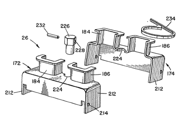
Continuing with the discussion of the plug 26, and referring
now most particularly to Figs. 1, 2 and 3, a pair of opposed
mating clam shell covers 172, 174 overlie and enclose the
rear end of the housing 97. Each cover 172, 174 also
includes a pair of half collars 184, 186, respectively, which
mate to form full collars when the covers are closed. Each
full collar 184A, 186A, as illustrated in Fig. 1, defines an
outlet for a bundle 54 of coaxial cable leads 116 as they
extend from the coaxial terminals 80 for termination at a
distant location.
An H-shaped bracket member 188 is used to attach the clam
shell covers 172, 174 to the housing 97. To this end, it
includes a bight element 190 which overlies the partition 106
and a pair of spaced apart, parallel legs 192 which overlie
15 and are supported on upper surfaces 194 of the housing 97
coplanar with the upper surface of the partition 106. The
bight element 190 has a centrally disposed hole 196 which
overlies a bore 198 in the partition 196. Suitable cutouts
200 and 202 are formed in the legs 192 in order to
20 accommodate standoffs 204 and 206 extending beyond the upper
surfaces 194.
The opposed ends of the legs 192 are upturned to define feet
208, each formed with a mounting hole 210 therein. Opposed
end flanges 212 on each of the covers 172, 174 is provided
-20-
~29133~7
with a mounting hole 214. With ehe covers 172, 174
positioned over the aft end of the housing 97 with the
bracket member 188 positioned thereon, the mounting holes 214
in the end flanges 212 are aligned with the mounting holes
210 in the feet 208 enabling rivets 216 or other suitable
fasteners to be inserted and fastened thereto (see Fig. 3).
A jack screw post 218 has a smooth upper end which is freely
received through the bore 198 as far as permitted by an
intermediate annular flange 220, then followed by a lower
thread stem 222 which, as will be seen below, is threadedly
engageable with the jacksocket body 58.
With the covers 172, 174, positioned over the aft end of the
housing 97 and mounted on the bracket member 188, then swung
to their closed position as illustrated in Fig. 1, the free
end of the jack screw post 218 extends rearwardly through the
bore 198, the hole 196 and through the semi-circular cutouts
224 formed in the covers 172, 174. Thereupon, an internally
bored jack handle 226 extends through the cutouts 224, and
the hole 196 into the bore 198 and over the upper end of the
jack screw post 218 until a diametrically extending aperture
228 is positioned so as to be aligned with a similar aperture
230 in the upper end of the post 218. A roll pin 232 is
fittingly received through the apertures 228, 230 and serves
to join the two parts together. When this has been
accomplished, securing straps 234 are receivable around each
collar 184A and 186A and drawable into contiguous
-21-
lZ98367
relationship therewith to thereby hold the covers 172, 174 intheir closed positions. Annular flanges 236 provided at the
extremities of the collars 184A, 186A serve to prevent
inadvertent removal of the straps 234 from the ends of the
collars.
With reference now to Figs. 9, and 13-15, a holding block 238
is illustrated which may be of any suitable material having a
plurality of through bores 240 therein with the same
arrangement or design as the bores 66 and 68 in the base
10 member 28 of the receptacle 22. The bores 240 receive the
nose ends of the pin contacts 50 and 52 in the same
relationship that they are to assume when they are inserted
into the mounting holes 66 and 68 in the base member 28.
Thus, all of the bores 240 receive an associated pin contact
50 or 52 and, in each instance, the associated barrel
portions 72 and 84 engage an undersurface 242 of the holding
block.
As seen in Fig. 13, actually two holding blocks 238 are
employed with each receptacle 22. That is, a holding block
238 is intended for temporary insertion into each of the
opposed end cavities within the receptacle separated by the
partition 44. At laterally disposed ends of each hold~ng
block 238, there is provided a handle member 244, a guide key
246, and a resilient locking finger 248 with a locking tab
250 at its extreme end. The inner surfaces of the sidewalls
1~8367
38 are formed with guide slots 252 to slidably receive the
guide keys 246. Additionally, windows 254 are provided in
the sidewalls 38 at two different elevations adapted to
receive the locking tabs 250 therein.
The holding block 238, with the pin contacts 50 and 52
mounted thereon, is then moved into its associated
compartment within the receptacle 22 until the tips of the
tails 82 of the pin contacts 50 are received in and extend
through their associated mounting holes 66. A chamfered rim
256 (see Fig. 16) serves to guide the barrel portions of each
pin contact 50, 52 into its associated mounting hole 66, 68,
respectively, in the event it is somewhat skewed. The same
situation exists with respect to the tips of the tail ends 82
of the pin contacts 52 and their associated mounting holes
68. In either case, it may be desirable for the mounting
holes 66 and 68 not to be through holes, but to require the
tips of the tail ends 82 and 88 to punch through a thin
remaining membrane at the bottom of each to aid in centering
and holding the tail ends properly positioned relative to the
base member 28. At the very least, a necked down cone of
material 258 with a reduced opening therethrough for fitting
reception of the tails 82, 88 is provided for this purpose.
It may be desirable for a manufacturer to assemble the
components in the manner illustrated at the right hand side
of Fig. 9 but without the receptacle 22 being mounted on the
-23-
129~1367
PCB 24. In that event, it would be up to the user to install
the pin contacts 50 and 52 to the PCB at a later time of his
choosing. The mutual construction of the holding block 238
and receptacle 22 just described is used to accommodate this
goal. Specifically, when all of the pin contacts have been
mounted in the holding block 238 with their nose ends 74 and
86, respectively, received in the through bores 240 and with
their barrel portions 72, 84, respectively, butted against
the undersurface 242, the holding block is moved toward and
into engagement with the receptacle 22 such that the guide
keys 246 on each handle member 244 is slidably engaged with
its associated guide slot 252 of the receptacle. The locking
tabs 250 at the ends of the locking fingers 248 are first
cammed inwardly by the sidewall 38, then spring outwardly
into engagement with its associated upper tier window 254.
With the holding block 238 in this position, the extreme tips
of the tail ends 82, 88 are firmly held by their associated
cones of material 258~ The mutual engagement of the tabs 250
and their associated windows 254 serves to maintsin the
relative positioning of the holding block 238 and the
receptacle 22 until a further operation is desired.
Subsequently, when it comes time to install the pin contacts
50, 52, into the PCB 24, pressure on the holding block in the
direction of the base member 28 causes the tabs 250 to be
cammed out of engagement with the upper tier of windows 254.
-24-
:1298367
The holding block 238 with its cargo of pin contacts 50, 52
is then moved toward the base member 28. With the receptacle
22 mounted on the PCB 24 as illustrated in Figs. 9, the tail
ends 82 and 88 are caused to pass through the metallized
S holes 70 and 71, respectively, until they achieve the finally
disposed relative positions illustrated at the left hand side
of Fig. 9. With the tips of the tail ends 82 and 88
protruding through the underside of the PCB 24, the PCB can
be subjected to a wave of solder in a known manner to
mechanically and electrically couple the pin contacts to
their associated circuitry on the PCB 24. Thereupon, the
holding blocks 238 are withdrawn from the receptacle 22 and
dlscarded, or set aside for future use.
Thereupon, as seen in Figs. 3 and 6, the receptacle is
fixedly mounted onto the PCB 24 by means of the jacksocket
body 58 and mutually threaded nut 64. Then, with the
receptacle 22 thus firmly secured to the PCB 24, the plug 26
is advanced toward mating engagement with receptacle 22 such
that guide keys 246A and 262 formed on the housing 97 will
20 slidingly engage with guide slots 252 and 264 to thereby
assure proper engagement therebetween. Thereupon, by turnlng
the jack handle 226 the threaded stem 222 of the jack screw
post 218 is threadedly engaged with the upper end of the
~acksocket body 58 and continues to be turned until the plug
26 is firmly, fixedly mounted into the receptacle 22. When
-25-
1~98367
this occurs, all of the pin contacts 50 are mechanically and
electrically engaged with the inner sleeves 78 of their
associated coaxial terminals 80 and the ground pin contacts
52 are mechanically and electrically connected to their
associated second sockets 94 in the grounding block 96.
Since the ground pin contacts 52 are longer than the signal
pin contacts 50, complementary bores 266 are formed into a
foreside 268 of the housing 97 (see especially Fig. 5) to
accommodate the additional length. The connector assembly 20
is now in a condition to transmit electrical signals.
It is desirable to provide an outer protective covering 260
for each bundle of leads 54. While shrink tubing could be
used, it is difficult and time consuming to thread a large
number of leads through such tubing. Furthermore, the
original shrink tubing would have to be cut off and removed,
then all of the leads uncoupled and inserted into new shrink
tubing each time it is necessary to work on or replace an
individual lead. Accordingly, suitable zipper-type tubing of
the type generally illustrated in Fig. 10 is preferred since
it can be applied and then unzipped, and reused as many times
as necessary without affecting those leads which are not of
concern.
Although there are numerous benefits which flow from the
invention, a primary benefit resides in the construction
-26-
..
1298367
according to which a high density of contacts can be joinedin one step to a receiving PCB while assuring that impedances
are matched between each incoming lead, its connection, and
the circuit board. As the plug 26 moves toward engagement
with its mating receptacle 22, the contact members 92 of the
ground pin contacts 52 first move into engagement with the
grounding block 96 to initially discharge any static
electricity which may be present. Thereupon, the contact
members 76 of the signal pin contacts 50 engage their
associated inner sleeves 78 of the coaxial terminals 80.
When the plug 26 reaches its final position within the
receptacle 22, the contact members 92 engage the grounding
block 86 at a region which i8 nearer the PCB 24 than the
location of engagement between the contact members 76 and
lS their associated inner sleeves 78. This construction
minimizes the possibility of ground loops which can be
destructive to the circuitry.
By reason of the design which is best illustrated in Fig. 6
of the reLative positioning of the contact members 90, 92 and
76, the thln construction of the base member 28, together
with the use of air as the dielectric in the coaxial terminal
80 and the positioning as best illustrated in Fig. 2A of
surrounding each signal pin contact 50 with four ground pin
contacts 52, all of these features result in maximum
electromagnetic shielding for each of the signal wires,
-27-
12g8367
assuring a controlled minimal impedance, and a low noise
level in my line which may be in close proximity to any
number of "active" lines.
While a preferred embodiment of the invention has been
S disclosed in detail, it should be understood by those skilled
in the art that various modifications may be made to the
illustrated embodiments without departing from the scope as
described in the specification and defined in the appended
claims.
-2~-