Note: Descriptions are shown in the official language in which they were submitted.
~3~3Z54 ~ 6-SM3-427
PLATEN ASS~M~Y ~OR A YACUUM PROCESSING SYSTEM
The present invention relates to the coating of thin
substrates under vacuum, and more particularly to a
modular sputtering system which is capable of sputter
coating substrates either serially or in a selective
access sequence.
In the fabrication of relatively small disk shaped
objects, such as semiconductor wafers or data storage
disks, multi-layered coatings must be applied to their
surfaces in order to achieve certain properties or
objectives. For semiconductor wafers a multi-layered
conductive coating serves to provide electrical contact
to the active portions of the circuit i.e., the
resistors, capacitors, diodes and transistors J and
further serves to interconnect these to provide a
functional circuit. For a data disk, the multi-layered
coating may consist of a magnetic layer for data storage
and an overlayer to provide protection for the storage
layer, The apparatus used to achieve such coatings have
traditionally been classified into two types; batch
coaters and single substrate coaters. Batch coaters
process a multiplicity of substrates in a single coating
operation whereas single substrate coaters sequentially
process individual substrates one at a time. This
invention relates specifically to the achievement of
multi-layered sputter coatings where the individual
substrates are sequentially coated.
The sputter coating process re~uires an environment
wherein a gas or gas mixture is maintained at a
sub-atmospheric pressure. This gas is frequently argon
which is preferred because of its chemical inertness and
low cost, but gas mixtures may be used. For this
~3~3254
reason, the coating apparatus must be capable of
maintaining a sub-atmospheric pressure o~ typically 1 to
30 millitorr pressure, where atmospheric pressure is 760
Torr. Since residual atmospheric gases such as oxygen,
nitrogen and water vapor can react with and contaminate
the freshly deposited coating, the chambers which make
up a sputter coating apparatus must be evacuated by
means of a pumping system such that chamber atmospheric
gas partial pressures of 10 7 Torr are routinely
achievable, prior to the coating process, and maintained
during the coating process as well as during the time
interval between layer depositions. Finally, since
different sputt~r coating process require different gas
pressures or gas mixtures, it is desirable that some
means be provided for achieving this diversity of
process environments without cross-contamination.
One means of achieving thess conditions is to
configure the sputter coating apparatus with a central
evacuated substrate handling or staging chamber with a
valved means of accessin~ multiple process chambers, as
well as a vacuum load-locked means of transporting
wafers to and from the ambient environment. While such
systems are commercially available there are several
problems associated with such systems.
In a typical state-of-the-art system substrakes are
processed in a generally cylindrical central substrate
handling chamber which is continuously evacuated by
means of a vacuum pump. Surrounding the central
substrate handling chamber are separately pumped process
chambers and a separately pumped load lock. Interior to
the central substrate handling chamber is a substxate
handling robot which is capable of three degrees of
motion, radial (R~, circumferential (~ and vertical
~L303254
(Z). The processing of substrates is accomplished in
the following steps. First, the interior hermetic door
which is capable of isolating the handling chamber from
the load lock chamber is closed and lock vented to the
atmosphere. Following this, the exterior hermetic door
is opened to admit either a sin~la substrate or a
multiple-piece batch of substrates separately racked in
a standard plastic cassette or the like. Thereafter,
the outer hermetic door is closed and the load lock
chamber evacuated until a predetermined degree o~ lock
chamber evacuation is achieved, whereupon the inner
hermetic door is opened to pxovide substrate access by
the three-axis central substrate handler. ~ single
substrate is extracted from the rack by an outward
radial traverse o~ the robot arm. This places the
substrate pick-up end of the wafer handler arm between
adjacent substrates on the rack. A short upward Z
t~averse then lits the substrate off its edge supports
and the subsequent radial retraction of the robot arm
carxies the wafer to a position interior to the central
substxa~e handling chamber. From this position, a~-
motion allows the substrate to be carried to a position
where it is aligned with a slot-shaped access port to a
process chamber. A hinged hermetic door separating the
process and central chamber then opens to allow radial
extension of the substrate handler arm and the
accompanying thrust of the substrate into the process
chamber. The subsequent downward Z motion places the
wafer on edge supports and the subsequent retraction of
the substrate handler arm allows for the reclosin~ of
the process chamber door and the hermetic isolation of
the substrate in the separately pumped process chamber.
The repetition of the above described actions allows for
~303254
the sequential placement of the substrate in any one or
all of the process chambers~ thus allowing for
sequential deposition of different layers without
interlayer exposure to the atmosphere. Upon completion
of the coating process, the substrate is returned to its
position in the load lock rack which then allows for the
eventual vent back and return to the atmosphere of the
entire rack-full of coated substrates.
One disadvantaga inherent in the configuration is
the fact that the load lock evacuation occurs serially
with respect to the coating process. Thus, any
lengthening of the load lock cycle which may be required
for minimization of particulate contamination, or
minimi~ation of reæidual gas transfer to the central
substrate handling chamber caxries with it the penalty
of reduced productivity. Related to this is the similar
restriction that the time constraints and engineering
limitations do not permit the batch heating of the
substrates in the lock. This limits the effective
removal of adsorbed contaminants from the substrate
surface prior to its introduction into the contamination
sensitive portions of the coating apparatus. Thus a
high level o contamination can find its way into the
coating process.
Another disadvantage of this configuration has to do
with the increased mechanical complexity introduced by
the requirement that the central wafer handling robot
have a radial motion capability. This requirement
introduces the need for mechanisms and bearings to be
present in the vacuum environment of the central
substrate handling chamber where contamination
considerations do not permit the use of lubricants.
Accordingly, these mechanisms become prone to the
~303254
generation of particulate contamination which if allowed
to settle on the substrate surface will result in the
unacceptable generation of coating defects. Similarly,
these mechanisms are also prone to vibration which then
implies the need for some type of edge contact with the
substrate in order to maintain substrate placement
accuracy. For silicon wafer substrates, such edge
contact is a known source of ~articulate contamination.
A further disadvantage of the previously described
configuration is associated with the relatively large
process chamber volum0 which is required by the need to
provide rotational means inside this chamber for placing
the substrate in a vertical attitude. This increased
process chamber volume results in a lengthening of the
evacuation time neeaed before the substrate can be
transferred back into the central wafer handling chamber
without substantial risk of contamination. This need
for increased dwell time in the process chamber reduces
the productivity of th~ coating apparatus. Similarly,
the larger relative volume of process to central
handling chambers, implies a higher level of central
handling chamber contamination at the chosen degree of
process charnber evacuation where substrate trans~er is
carried out. This results from the fact that gaseous
contaminants experience a dilution upon migrating from
the process to the central handling chamber, which
dilution decreases as the process chamber is made large
relative to the central handling chamber. For both
these above reasons~ an apparatus configuration having
large process chambers has a higher potential for
residual gas cross-contamination.
32S4
To overcome the above shGrtcomings the present
invention provides a central substrate handling or
staging chamber with separately pumped process chambers,
and dual load lock chambers which are alternately loaded
with multiple-piece substrate batches (25 pieces being a
standard batch of semiconductor wafers), using an
external substrate handling robot. Accordingly, while
one substrate batch is undergoing load lock evacuation,
the second batch, having been previously evacuated, is
accessible to the central wafer handling robot for
purposes of execution of the coating process. For this
reason, load lock dwell times are ordered parallel to
the coating process and extended load lock dwell times
do not impair apparatus productivity until the batch
lock dwell time exceeds that time needed for the serial
coating of a full batch of individual substrates. The
benefit of this increased permissible lock dwell time is
enhanced by the provision of means for heating the
substrate batch. Thus~ batch evacuation and thermal
desorption are both accomplished before the opening of
the interior load lock door which individually opens a
given lock chamber to the central handling chamber.
Upon completion of this lock cycle, the opening of
the interior lock chamber door allows the substrate rack
to be accessed by a substrate handling robot located
inside the separately pumped central wafer handling
chamber. In accordance with the invention the wa~er
handling robot is provided with only a circumferential
~) and vertical (Z) translation capability.
Accordingly, the previously described pick-up and place
action permits individual substrates to be extracted
from the metal rack, carried along the circular path and
placed down on a series of two-position platens located
~3032S4
on the circular path. Once the substrate has been
transferred and the wafer handler moved away, a clamp is
activated to cause the substrate to be held near its
edge and pressed against the platen surface. Thereupon,
the platen is caused to pivot 90. This action causes
the substrate to be placed vertically and thrusts it
through a large opening in ~he central wafer handling
chamber. Located opposite this opening is the
sputtering source, hermetically mounted to the exterior
wall of a separately pumped process chamber. This
previously described pivoting motion also causes a
hermetic seal to be effected between the platen housing
and the interior wall of the central substrate handling
chamber. This seal, located at the periphery of the
large circular opening in the central substrate handling
chamber, effectively isolates the process chamber from
the central substrate handling chamber. Once this seal
has been accomplished, ~he previously described sequence
of sputter gas introduction, and application of
sputtering source power, causes the substrate to become
coated. Similarly, post-deposition re-evacuation of the
process chamber, and the subsequent reverse pivot of the
substrate platen opens the interchamber seal, and allows
the unclamping and transfer of the substrate to another
platen where the entire process is repeated to cause a
second sputter-deposited layer to cover the first. By
repetition of this action the substrates can be
se~uentially carried through a series of isolated
process chambers where any desired combination of
coating and etching operations may be performed. Once
an entire batch has been sequentially processed and
returned to the load lock rack, the load lock is sealed,
vented back to atmospheric pressure, and the batch
~303254
returned to the original plastic cassette from whence it
had heen extracted.
In addition to the dual batch load lock
configuration, this configuration has the following
advantages. (A~ the central wafer handling robot~
having no radial motion mechanism is capable of very
smooth particulate free wafer transfer; (B) the
individual process chambers are much smaller permitting
much more rapid, contamination-free transfer of wafers
through the se~uences leading to the multi-layared
substrate coating; and (C) the combination of this
serial coating processing with parallel batch lock
operation uniquely achi'eves a very high level of purity
with regard to residual atmospheric gases.
Other advantages of the invention will be apparent
from the following description when considered in
connection with the accompanying drawings, wherein:
Fig. 1 is a perspective view of the sputtering
system of the invention, with portions removed or cut
away for clarity;
Fig. 2 is an elevation view, with parts cut away, of
the load locks of the invention;
Fig. 3 is a sectional view of the wafer handling
assembly of the invention;
Fig. 4 is a sectional view taken along line 4--4 of
Fig. 3.
Fig. 5 is a sectional view of the wafer handling arm
of the invention;
Fig. 6 is a plan view of the wafer handling arm;
Fig. 7 is a view, shown partly in section of a
platen assembly of the invention;
Fig. 8 is a plan view of the platen assembly;
Fig. 9 is a sectional view taken along line 9--9 of
Fig. 8;
13~3Z~
g
Fig. 10 is a rear elevation view of a platen
assembly with parts shown in section to illustrate an
atmospheric clamp assembly of the invention;
Fig. 11 is a schematic side elevation view of the
platen assembly positioned at a process chamber;
Fig. 12 is a fragmentary sectional view of a clamp
assembly of the invention; and
Fig. 13 is a Eragmentary view along line 13--13 of
Fig. 12.
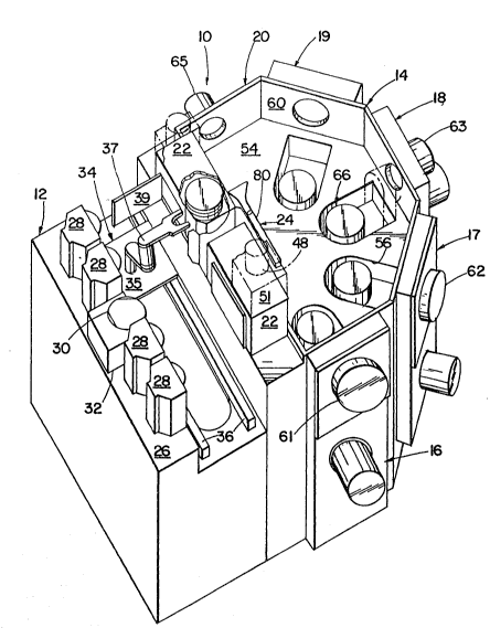
Referring to Fig. 1, there is illustrated a
sputtering system, designated generally by the numeral
10, which includes a loading station 12 at atmospheric
pressure, an evacuated central handling or staging
chamber 14, a plurality o evacuated process chambers
16, 17, 18, 19 and 20, first and second load lock
chambers 22 located between the staging chamber and the
loading station, and a wafer handling assembling 24
located within the staging chamber. A top plate and
removable cover (not shown) are received over the
staging chambcr to enclose the chamber for vacuum
processing. For purposes of illustration herein the
substrates to be sputtered will be described as
semiconductor wafers, although it will be understood
that the present invention can be used to coat other
forms of substrates such as audio discs.
LOADING STATION
In accordance with a preferred embodiment of the
invention the loading station comprises a platform 26
which receives four standard wafer cassettes 28 loaded
with wafers 30, a flat finding station 32 which
pre-orients each wafer with the flat in a predetermined
angular position, and a handling assembly 34. As
illustrated herein the handling assembly 34 comprises a
~3~32S~
-- 10 --
platform 35 which is movable along rails 36 extending
along the open faces of the cassettes 28, and an
articulated wafer picking arm 37 mounted on the platform
35; however, it can be appreciated that a multi-axis
robot system can also be used. The components of the
loading station are well-known and commercially
available items, and will not be described in further
detail herein.
LOAD LOCKS
The load locks 22 are identical and are described
interchangeably herein. In Fig. 2, the load locks are
viewed from inside the staging chamber 14. Referring to
Yigs. 1 and 2, the load lock 22 is a two level structure
including an upper level 38 having an access door 39
facing the loading station and a lower level 40 opening
into the staging chamber 14 to provide access to the
waers 30 by the wafer handling assembly 24. Within the
load lock there is mounted a rack ~1 which includes a
plurality of spaced-apart metallic wafer supporting
elements. Each rack holds a standard cassette-load of
twenty-five wafers and is received on an elevator 42
which is operable to position the rack at the upper
level 39 to receive wafers transferred from the
cassettes by the arm 37, and to move it downward to the
lower level 40 in position to be accessed by the
handling assembly 24. To maintain the vacuum integrity
of the chamber 14 when an elevator is in the up position
as shown on the left side of Fig. 2, the base 44 of each
of the rack/elevator assemblies 41 defines a valve
element which is operable to seal the opening between
the uppex and lower levels of the load lock.
~30325~L
- 11 -
The elevator actuating mechanism 46 is mounted below
the chamber 14, and a bellows 47 surrounds the actuating
shaft of the elevator to prevent vacuum loss. A poppet
valve unit 48 is mounted atop the chamber and has a
valve element ~9 which is operable to open and close a
port 50 between the chamber 22 and an upper plenum 51.
A cryogenic pump 52 operates to evacuate the plenum 51
and chambers 22, while a poppet valve 53 controls the
inlet to the pump.
Also mounted within the load lock chambers 22 are
radiant heating units ~5 disposed vertically on opposite
sides of the rack 41. Preferably the heating units
comprise a plurality of quartz halogen heating lamps
such as those manufactured by USHIO INC. and designated
as series QIR. When a rack is fully loaded and the load
lock closed and evacuated, the heaters are effective to
remove adsorbed contaminants rom the waer surfaces
prior to the entry of the wafers into the staging
chamber 14.
In operation, a cassette-load o wafers 30 is
transferred, one-at-a-time, from one of the cassettes
28, to the flat~finder 32 and then to the rack 41 by
means of the wafer handling assembly 34. The door 39 is
then closed and the chamber partially evacuated using a
mechanical roughing pump (not shown~. One of the valves
49 is then opened and cryogenic pump 52 is activated to
evacuate the open load lock 22 to a pressure approaching
that of the chamber 14. Valve 53, shown in the open
position in Fig. 2, is provided to close the inlet to
the pump 52 for maintenance and regeneration o~ the
pump. The heaters 45 are then energized to effect a
batch degassing of the wafers. The valve 49 is then
clGsed and the elevator 42 is moved downward to the
~303254
position shown on the right side of Fig. 2, the downward
movement opening the valve element 44 and thus opening
communication between the right side load lock 22 and
the staging chamber 14. At this point a rack load of
wafers are in position to be accessed by the wafer
handling assembly 24 as will be described in more detail
below.
As noted above, the plenum 51 communicates with both
load locks 22 the loading, evacuating, heating and
transfer functions for both of the load locks being
essentially the same as that described above.
STAGING CHAMBER
Referring to Fig. 1, the staging chamber 14 is
essentially octagonal in plan view with three sides of
the octagon cut off by the plane defined by the ~ace of
the load lock chamber. The bottom o the staging
chamber is a plate 54 with a plurality of wells 56
formed therein arranged in a circular pattern about an
axis defined by the axis of the handling assembly 24.
The side walls 60 define interfaces between the staging
chamber and the individual process chambers 16-20, and
the top of the chamber is defined by a readily opened
and removable cover, which is not shown herein in the
interest of clarity.
Each of the chambers 16-20 could be used to perform
any one of a number of different processes such as
etching, or sputter coating. For example, a plasma etch
unit 61 can be installed at chamber 16 and sputter
sources 62 and 63 installed at process chambers 17 and
18, with chamber 19 having another sputter source (not
visible) and chamber 20 being used as a vacuum pump
13~)3Z5~
- 13 -
station, with a vacuum pump 65 installed therein. It
can be appreciated, however, that with relatively little
modification chamber 20 could be employed as a
sputtering or other processing station with the vacuum
pump communicating with the staging chamber through, for
example, the bottom plate 54.
Within each of the wells 56, there is mounted a
platen assembly 66 (shown schematically in Fig. 1),
which is pivotable from a wafer transfer position shown
in solid line in Fig. 1, to an operating position shown
in broken line only at process station 18. As will be
discussed in detail below, the platen serves both as
means for retaining wafers and as a valve for isolating
the process chamber from the staging chamber when the
wafers are being processed, or when a particular process
chamber is undergoing maintenance.
Wafers are transferred between the load locks 22 and
~he process chambers 16-19, or from one o the process
chambers to any one of the other process chambers by
means of the wafer handling assembly 24.
WAFER ~NDLING ASSEMBLY
Referring to Figs. 3 and 4, there is illustrated the
wafer handling assembly 24, comprising a mounting flange
assembly 68 received in an opening 70 formed through the
bottom plate 54 of the staging chamber, a support plate
72 attached to and depending from the flange assembly, a
ball screw linear drive system supported by the plate 72
and designated generally by the numeral 74, a drive
shaft assembly 76 mounted on the drive system for linear
movement i.e. the required Z a~is movement of the
handling assembly, a rotary drive system 78 mounted on
~L3a~32S4
the shaft assembly to provide the ~-movement of the
handling assembly, and a handling arm 80 attached to the
shaft assembly and adapted to receive wafers ~or
transfer to and from the process stations and the load
locks.
The support plate 72 is essentially a channel as
shown in plan view in Fig. 4, to which the movable
elements of the wafer handling assembly are mounted,
including the linear drive system 74 and the rotary
drive system 76.
The linear drive assembly 74 comprises a housing 82,
also in the form of a channel, which supports the drive
shaft assembly 76 and the drive system 78, pairs of
bearing carrîers 83, and 84 attached to the housing, a
pair of rails 85 and 86 attached to the plate 72 on
which the bearing carriers are supported, and a ball
screw drive assembly designated generally by the numeral
88.
The bearing carriers 83-84 enclose low-~riction
linear bearings which ride on the rails 86. The ball
screw drive assembly 88 comprises upper and lower
spacers 89 and 90 attached to the plate 72, a lead screw
92 mounted or rotation in the spacers, a ball nut
assembly 94 attached to the housing 82, and a drive
system 96. The ball nut assembly 94 cornprises a support
block 98 fixed to the housing 82 and attached to a ball
nut unit 100 of the ball screw assembly. As is well
known in the art, rotation of the lead screw 92 within
the ball nut assembly 94, causes the housing 82 to move
up or down along the rails 85, 86 depending on the
direction of rotation of the screw. Ro~ation of the
lead screw 92 is provided by a motor and gear unit 102,
mounted on a support bracket 101 attached to the plate
~L3~32~;4
- 15 ~
72, which drives the screw by means of a timing belt
104. A brake 105 fi~ed to the plate 72 and operating on
the lead screw 92 maintains the position of the linear
drive system in the event of a 105S of power. A shaft
encoder 103, also driven by the motor 102 provides Z
motion information to a control system for the handling
assembly.
The rotary drive system 78 comprises a drive motor
106 supported by a plate 107 welded to the housing 82,
an output shaft 108 coupled to the motor output shaft, a
rotary seal assembly 110 surrounding the shaft 108, a
bellows assembly 111, and the handling arm 80 attached
to the end of the output shaft.
A cylindrical housing 112 depends from the mator
106, and a brake 114, similar to the brake 105, is
mounted on the housing and is coupled to the motor
output shaft. A shaft encoder 116 also driven by the
motor 106 is mounted on the housing 112 to provide O
motion informa~ion to the control system.
Since the area above the plate 5~ is under vacuum,
the sealing o~ the drive assembly to prevent vacuum
loss, and to avoid conta~ination of the handling chamber
is very ;mportant. To this end the rotary seal assembly
110 provides a highly reliable means to isolate the
rotating components from the vacuum system, while the
bellows eliminates the need for sliding seals. The
rotary seal is preferrably a type of seal referred to as
FERROFLUIDIC, which is a registered trademark of
FERROFLUIDICS CORPORATION, which is well known in the
art and will not be described in detail herein. As
illustrated in the preferred embodiment shown in Fig.
3. The rotary seal is enclosed within a cylindrical
housing 124 which is suspended from an end member 125 of
~3Z54
- 16 -
housiny 82 and sealed thereagainst by means of an O-ring
126. The housing 124 includes an elongated cylindrical
extension 128 which supports the output shaft 108
through a lower bearing 129 and an upper bearing (not
shown) within an end cap 130 of the housing 124.
As illustrated in Fig. 3, the handling assembly must
undergo significant vertical or Z axis travel in order
for the handling assembly to access a full cassette load
of wafers positioned on the racks 41. To accommodate
this motion without employing sliding seals, the sealed
bellows assembly 111 is installed between the drive
system housing 82 and the plate 54 which defines the
floor of vacuum chamber 14. The bellows assembly
comprises an upper flange 132 which is attached to the
top member of the flange assembly 68 and sealed
thereagainst by an O-ring 133, a lower flange 134
attached to the end member 125 of the housing 82 and
sealed by an O-ring 135, and a metallic bellows 136
which surrounds the extended portion 128 of the rotary
seal assembly 116 and is fixed to the flanges 132 and
134 by welding or brazing or the like.
Referring to Figs. 5 and 6, the wafer handling arm
80 is a fabricated structured comprising a hub assembly
138 an arm structure 140 and a wafer-receiving paddle
142. The hub assembly comprises a substantially
rectangular housing 143 with a downwardly projecting hub
144 which fits over the end of shaft 108 and is attached
thereto by means of a key 145 and a yoke clamp member
146 which is received in an opening formed in the
housing and includes a portion partly encircling the
shaft, The clamp member is attached to the housing by
means of screws 147 (one of two shown). An O-ring 148
is received in a groove formed in the housing and seals
~3~32S4
- 17 -
against the shaft 108. A cover 149 bolted to the
housing closes the upper end of the housing and is
sealed thereagainst by an O-ring 157 received in an oval
groove formed in the housing.
The arm 140 is a fabricated metal box, rectangular
in cross-section, which is welded to the housing 143.
The outer end of the arm is welded to an end cap 155 to
which the paddle 142 is bolted. Referring particularly
to Fig. 6, the paddle 142 is a relatively thin,
substantially solid member which is bolted to the end
cap 155. The free end of the paddle is formed with arms
150 and 151 with the wafers 30 (shown in broken line in
Fig. 6) being supported on three contact points 152
distributed about a centerpoint 153 on the longitudinal
axis of the arm assembly. The paddle is relatively
thin, as noted above, to enable the paddle to fit
between wafers in the racks 41, and as shown in Fig. 6
the paddle is offset from the centerline of the arm
assembly to facilitate entry of the paddle into the
platen assemblies as will become more apparent from the
description below. It should be noted that the waers
are maintained on the arm by gravitational force only,
with no other restraint.
The paddle 142 includes three capacitive proximity
sensors 154 which are received in depressions formed in
the bottom surface of the paddle and distributed 120
apart at a radial location corresponding to the edge of
a wafer. The sensors protrude slightly above the top
surface of the paddle but below the pins 152. A fourth
sensor 154a is centrally located and is flush to the top
surface of the paddle. These sensors can be of a type
manufactured by Cox Enginsering Company and designated
as Model SR2 and will not be described herein in
~303Z~;4
detail. The central sensor serves to detect the
presence of a wafer on the paddle and the outer sensors
sense the position thereon. A slight deviation from the
position shown in Fig. 6 wherein the edge of the wafer
overlies the center of the three outer sensors will be
detected so that misalignment and potential damage of
the wafers when they are placed on a platen assembly can
be avoided.
The sensors 154 and 154a indicate wafer position by
producing a voltage level change in a binary manner,
i.e. high voltage at sensor 154a indicates that a wafer
is present; whereas a low voltage indicates no wafer.
Similarly, high voltage at all three of the edge
detectors 15~ indicates that the wafer edge is in the
proper location; whereas, low voltage at any sensor
indicates that the wafer edge does not properly overlie
the sensors. After a wafer is received on the paddle
both a wafer presence and proper wafer position signals
must be recei~ed before the arm is moved. If thq wafer
is tipped in any direction the wafer presence sensor
15~a will provide a proper signal, and a wafer presence
signal will be issued. If the presence condition is
satisfied but the wafer does not properly overlie the
sensors 154, the wafer will be returned to its present
status, the arm will be repositioned in a direction
dependant upon which of the three sensors failed to
provide the proper signal, and the wafer will be lifted
again to go through another position sensing sequence.
If proper positioning is sensed the paddle will be moved
to transfer the wafer to its next station. If after a
second try proper positioning cannot be established
manual intervention will be required to resolve the
error.
~3~25~
-- 19 --
It can be appreciatea that the insertion of
electrical components such as the sensors 154 into the
vacuum system can cause problems, particularly in
association with a rotating component such as the arm
assembly 80. In accordance with the invention the
electrical lines ~or the capacitive sensors,
collectively designated 15Ç, are routed to connecting
points below the staging chamber through the center of
the hollow shaft 108, into the housing 143, through
plugs 158 within the housing, and then through the arm
140 to the paddle 142 where they extend through sealed
openings and are received within channels formed in the
underside of the paddle. As described above, the area
below the plate 54, including the interior of the shaft
108 are at atmospheric pressuxe; however, the O-rin~s
148 and 157, and an O-ring 159 between the end cap 15
and the paddle, along with the sealed openings in the
paddle, maintain the integrity of the vacuum within the
chamber 14.
In operation, the handling assembly is initially
positioned adjacent to a rack 41 within one of the load
locks 22~ Then the motor/gear unit 102 is energized to
rotate the lead screw 92 and drive the housing 82 upward
to position the arm assembly 80 vertically in position
such that the wafer paddle 142 is slightly below a
selected wafer within the rack 41. The rotary drive
motor 106 is then energized to rotate the arm until the
paddle is aligned beneath its selected wafer. The
linear drive system is again actuated to raise the arm
slightly to engage the wafer wîth the contact points
152. The arm is then rotated out of the load lock and
lowered to the Fig. 3 position, after which th~ rotary
drive system is again energized to rotate the paddle to
32S4
- 20 ~
a position over any one of the platens 66 to deposit the
waer thereon for processiny, as will be described in
detail below.
PLATEN
Referring particularly to Figs 7, 8 and 9, there is
illustrated the platen assembly 66 of the invention. In
accordance with the invention the platen assembly
comprises an essentially enclossd housing 162, a pivot
assembly 164 attached to the end of the housing, and a
platen 166.
The housing 162 comprises an upper support plate
168, a support ring 170 welded to an arcuate member 171
which in turn is welded to the upper support plate, a
lower support plate 172 which can be integral with the
upper plate, a lower ring 174 welded to the plate 172
and a side wall member 176 which encircles the rings 170
and 174 and is welded thereto, and which extends outward
from the ring members to cover the open sides between
the support plates 168 and 172, to which it is also~
welded. A cylindrical cover 178, including a disk 179,
a tube 180 welded to the disk, and a ring 181 welded to
the tube; is bolted to the ring 174.
The pivot assembly 164 comprises an elongated
housing 182 (see Fig. 10) bolted to the ends of the
support plates 168 and 170, hollow stub shafts 184
welded to the housing and extending through seal and
bearing units 160 received in the well structure 56 the
seals prsferably being FERROFLUIDIC seals. The well
structure is in the form of a first sealed box structure
161 having the rounded-end rectangular shape illustrated
in Fig. 1, with a secondary cylindrical box structure
13(~3254
- 21 -
163 attached thereto to provide clearance for the bottom
portion of the platen assembly. The bearing units 160
extend through the sides of the first box structure 161,
and one of the stub shafts is connected to a drive
system designated 16S which can be in the form of air
cylinder and lever arm system as shown schematically in
Fig. 10, and which is operable to move the platen
between its horizontal loading position and its vertical
operating position.
Referring particular to Figs. 7, 8 and 9, the platen
166 comprises an annular frame member 186 which is
fastened to the ring 170 by means of screws (not shown),
a wafer support assembly 190 clamped to the frame member
186, and a wafer clamp assembly 192 supported by the
frame member 1~6 and mo~able relative thereto to
selectively clamp a wafer to the support assembly 190
and to release it therefrom.
The wafer support assembly 190 comprises a
relativel~ thick, essentially solid circular platen
element 19~; a lower ring member 196 spaced from the
platen 194; a relatively thin, tubular member 198
connecting the platen 194 and ring 196 and welded
thereto; and a clamp ring ~00 which is fastened to the
ring 196 by screws ~01 and which clamps the wafer
support assembly 190 to an inwardly projecting flange
portion of the lower ring 196 through insulating rings
199 .
A circular plate member 202 is fastened to the
bottom of ring 196 and substantially closes the bottom
of the support assembly 190. The plate 202 has an
annular channel 203 formed therein which is closed by a
ring 204 to define an annular cooling water channel.
~3()3254
- 22 -
An electrical resistance heater unit 208 is fastened
to the platen 194 by a bolt~spring washer assembly 211
and includes a circular heating element 209 in contact
with the platen 194. A temperature probe 210 is
received through the heating element 208 and is imbedded
in the platen 194 just below the wafer receiving
surface. A gas line 212 is received through the plate
202 and e~tends through the platen 194 to communicate
with one or more channels 214 formed in the surface of
the platen to supply gas to effect gas conduction
cooling of a wafer 30 received on the support assembly.
The remaining volume between the platen 194 and the
plate 202 is filled with a thermal insulating material
216.
WAFER CLA~P
Reerring to Figs. 8 and 9, wafers 30 are retained
on the platen assembly for processing by a clamp system
mounted on the platen~ The clatnp system comprises an
annular actuating cylinder assembly 222 supported by the
frame member 186, and the clamp asse~bly 192, which is
supported by the frame and actuated by the cylinder
assembly 222.
The cylinder assembly comprises an annular member
226 attached to the frame member 186 by bolts 227, and
having an annular recess formed therein to dsfine a
fluid cylinder 228. A sealed cover member 230 covers
the open end of the cylindrical member 226 and is
fastened thereto by the bolts 227 to sealingly enclose
the cylinder 228. An annular piston 232 is received
within the cylinder 228 and is sealed therein by inner
and outer O-rings 233 and 234. Looking at the right
13032S4
side of Fig. 9, there is illustrated one of three piston
ro~ assemblies 236 attached to the annular piston 233.
The piston rod assembly comprises a rod 238 extending
through the piston and the cover member 230 and press
fit to the piston. The shaft is sealed at the lower end
of the cylinder by an O-ring 239 retained in place by a
bearing cap 240 which aligns and supports the lower end
of the piston rod, and at its upper end by an O-ring
received in an insert 242 retained by a bearing cap 244
captured between the cylinder 226 and the frame member.
An O-ring 245 provides a static seal between the cap and
the frame.
The upper end of the shaft 238 has a reduced
diameter portion which is received through a disc 248
and through an insulating ring 246 attached to the clamp
assembly 192, the ring and disk being clamped between
the shoulder formed by the reduced diameter portion of
the shaft and a washer~nut assembly threaded onto the
end of the shaft. ~ hellows assembly comprising the
disc 248, the cap 244 and a metallic bellows 250 brazed
or otherwise attached to the disc and cap maintains
vacuum integrity. Fluid inlets ~not shown) above and
below the piston 232 permit the entry of fluid pressure
to the cyl;nder 228 to selectively move the rod 238 up
or down to actuate the clamp assembly.
The clamp assembly 192 surrounds the platen 194 and
comprises an upper ring 251 and a lower ring 252
maintained in spaced relation to each other by three
spring members 254 distributed about the clamp
assembly. The lower ring has a flange portion which is
attached to the insula`ting ring 246 by a plurality of
screws 253. The spring members provide compliance
between the wafer surface and the clamping plane when
1~3;~:54
- 2~ -
the clamp assembly engages the wafer. As best shown in
Fig. 7, a section 255 of the upper ring 251 is cut away
over about at 170 arc to provide access ~or the wafer
arm 80 to deposit wafers on the platen 194 when the
clamp assembly is in its up or retracted position as
shown in broken line in Fig. ~.
A plurality (preferably three as shown in Fig. 8) of
inwardly extending projections 256 are formed in the
upper ring to engage a wa~er for clamping to the platen
surface. When the clamp is in its retracted position
and a wafer is inserted through the opening 255 by the
arm 80 the wafers are deposited on a set of projections
extending inwardly from the upper ring below the
opening, including pins 257 extending radially inward
from the wall of upper ring and a finger 258 attached to
the outer wall of the upper ring and e~tending upward
into the opening and de~ining a plane with the pins.
To provide sealing o~ the platen assembly when it is
positioned at a process station O-rings 259 and 260 are
received in grooves formed in the face of the frame
member 186. When the arm 80 is pivoted into position to
place a wafer on the platen with clamp assembly in its
up position, the paddle 142 enters into the opening 255,
the arm assembly is lowered to deposit the wafer onto
the pins 257 and ~inger 258, below and the arm is
pivoted to another position away from the platen. Fluid
pressure is then applied to the cylinder 228 above the
piston 232 to move the piston downward, correspondingly
moving the clamp assembly downward to first deposit the
wafer on the platen sur~ace, then clamp it thereon.
When the wafer is in place on the platen the platen
assembly is pivoted upward to position the wafer in a
vertical position at the opening of a desired processing
1303254
- 25 -
station as illustrated in Fig. ll, which for purposes of
illustration is shown as a sputtering station including
a sputter source 262.
AT~OSPHERIC CLAMP
In normal operation the platen rotary drive provides
sufficient sealing force between the platen assembly and
the wall of the staging chamber when the platen assembly
is rotated to its operating position facing a process
chamber, as illustrated schematically in Fig. ll, since
the pressure differential between the evacuated staging
chamber and the evacuated process chamber is low. When,
however, a process chamber is undergoing maintenance
either in place or removed from the sputtering
apparatus, and operations are to continue at other
process stations, it is necessary to close the affected
process station, using the platen assembly as a door or
cutoff valve. In such instances there will be
atmospheric pressure acting on the outside of the
staging chamber, in which case it is considered
necessary to provide additional closure means to
maintain the vacuum integrity of the system.
Referring to Fig. 10, there is illustrated therein a
pair of clamp assemblies designated generally by the
numeral 268/ while Fig. 12 shows an enlarged view of one
of the clamp assemblies. The assemblies are essentially
identical and will be described interchangeably herein.
The clamp assemblies 268 are essentially toggle
clamps which are capable of applying a relatively high
closing force to the platen against the wall of the
staging chamber. Each toggle mechanism comprises a link
arm mount 280 welded to tbe underside of a top wall
13~)325~
- 26 -
member 281 of the staging chamber, a lock arm 282
pivotally attached at one end to the mount, and a
connecting or toggle arm 284 pivotally attached to the
opposite end of the lock arm, and to an actuating
mechanism designated generally by the numeral 286. A
wedge-shaped clamp surface member 278 (See Fig. 13) is
attached to the back surface of the ring 170, and roller
bearing 287 mounted on the end of the lock arm 282 rides
up the wedge 278 to transmit the clamping force of the
toggle assembly to the platen assembly and thus to side
wall 60 of the staging chamber.
The actuating mechanism 286 comprises a mounting
block 288 bolted to wall 281, and a manually operated
drive screw assembly 290. The drive screw assembly 290
comprises a screw 2g2 e~tending through the mounting
block and having a link end 293 fixed to the lower end
thereo for attachment to the connecting arm 284~ a
bearing 294 pressed into the mounting block 288, a drive
nut 295 threaded onto the screw and retained to the
bearing by a snap ring, a handle 296 pivotally attached
to the drive nut, and a vacuum bellows assembly 297
attached at its upper end to the mounting block and at
its lower end to the link end 293.
The handle comprises a yoke 298 which fits over
opposite flats o the nut and is pinned thereto, and a
rod 300 fixed to the closed end of the yoke, the handle
bein~ capable of being flipped over 180 from the
position shown. The bellows assembly 297 comprises an
upper flange 301 clamped to the block 288~ a lower
flange 302 clamped to the link end 293 and a metallic
bellows 303 welded to the flanges. O-rings between the
flanges and their associated mounting members maintain
the vacuum integrity of the clamp assembly.
1303;;~5~
- 27 -
Referring to Fig. 10, the right hand clamp assembly
is shown in its open position, and the left hand clamp
is shown in its closed position. The clamp assembly is
moved from the open to the closed position by rot~ting
the drive nut 295 with the handle assembly in a
direction which will cause the screw to move downward.
The downward movement of the screw causes the lock arm
282 to move to the closed position, with the connecting
arm 284 acting as to toggle to lock the assembly in the
closed position.
OPERATIO~
Cassettes 28 of wafers 30 are initially deposited on
the platform 26. At the commencement of a processing
cycle wafers are transferred one-by-one by the handling
assembly 34 from the cassettes to the flat finder 32 and
then to a rack 41 positioned within one or the other of
the load locks 22. Whe~ thè rack is fully loaded the
lock is pa~tially evacuated using pumping means not
shown, following which the corresponding plenum valve 49
is opened and the load lock is evacuated to the desired
level . When the desired vacuum level is reached the
heaters 45 are energiz~d to effect degassing of the
batch of wafers. While the batch in the first load lock
is undergoing the degassing process the rack in the
second load lock 22 will have been positioned in the
staging chamber 14 for transfer one at a time to
selected processing chambers.
When the degassing operation is complete the valve
49 in the first load lock is closed and the elevator 47
is actuated to move the batch of wafers from the load
lock to the staging chamber 14, which is maintained
~3~3~
- 28 -
under vacuum by a dedicated vacuum pump. At this time
processing of the batch originally in the second load
lock will have been completed and the processed wafers
returned to the rack on`the second elevator. The second
elevator is then actuated to return the batch of wafers
to the second load lock, whereupon the second load lock
is vented to atmosphere, and the wafers are returned to
a cassette 28 by the picking arm 37. A new batch of
wafers is then loaded into the second load lock as
described above where the evacuation and degassing
processes are carried out in preparation for further
processing.
When the rack 41 is within the staging chamber 14,
each of the wafers thereon is accessible by the wafer
handling assembly 24. Referring to Fig. 1, if the wafer
handling arm ao of the handling assembl~ 24 is in the
position shown, and the left side rack as viewed in Fig.
2 is positioned within the staging chamber, the arm 80
would ~irst be rotated clockwise ~from the Fig. 1
position) until the paddle 142 is positioned opposite
the rack. The arm 80 is then raised to position the
paddle just below the level of the wafer to be
processed, further clockwise to put the paddle directly
under the wafer, raised urther to lift the wafer off
the rack, and then rotated counterclockwise to extract
the wafer from the rack and lowered to a position
suitable for accessing the individual processing
stations 16-19. When the wafer is extracted, proper
positioning of the wafer on the paddle is verified by
the proximity sensors 152.
Once the wafer is extracted and proper positioning
verified the arm is rotated counterclockwise to position
the paddle over the platen at a desired one of the
13~)3254
- 29 -
processing stations 16-19. To accept a wafer from the
paddle, the platen assembly is put in its horizontal
position as shown in Fig. 7, with the clamp assembly in
its raised position as shown in Fig. 9. With the platen
so positioned, the arm 80 is rotated until the paddle
enters the opening 255 and the wafer is centered over
the platen 194. The arm is then lowered to deposit the
wafer on the two pins 257 and third pin 258 and the arm
is rotated to retract the paddle. The clamp assembly is
then moved downward to clamp the wafer against the
platen where it can then be preheated by contact with
the platen, which has been preheated by the heating unit
209.
For processing, the platen assembly is ro~ated from
the broken line position of Fig. ll to the solid line
position wherein the platen assembly sealingly engages a
wall of the staging chamber adjacent to a processing
chamber such as the sputterin~ chamber 18, whereupon the
chamber 18 can be evacuated by its dedicated pumping
system in preparation for processing. Upon completion
of processing the platen assembly is returned to its
horizontal position and the clamp assembly is positioned
for extraction o the wafer by the arm 80. The wafer
can then be moved to another station for further
processing, or if processing is completed, returned to a
rack 41 below one of the load locks from which they can
then be returned to cassettes on the platform 26 by
means of the elevator 47 and the handling assembly 34.
While the processing o one batch is being carried out,
the second batch of wafers can be undergoing the
degassing process.
~03~:5~
- 30 -
It is important to note in considering the above
sequence of events that from the time the wafers are
loaded onto the racks 41 until they are returned to the
cassettes after processing they are not subjected to any
direct radial movement. The arm 80 undergoes vertical
(Z) and rotational (~ motion only in transferring
wafers between the racks and the platens. This lack of
radial motion greatly reduces the potential for
misaligning the wafers in the transfer process and for
generating particulates caused by relative motion
between the wafers and the handling components. The
radial movement of the wafer which might ordinarily be
required to inject the wa~er into a processing chamber
is accomplished by the pivoting movement of the platen
assembly which also pexmits the platen assembly to serve
as a valve isolating the process stations from the
staging chamber, and orients the wafers in the desired
vertical position for processing.