Note: Descriptions are shown in the official language in which they were submitted.
1 3 ~ 2
BACKGROUND OF THE INVEMTION
Field of the Invention
-
The present invention relates to an apparatus for
correcting errors of digital data and, more particularly, to
an error correcting apparatus suitable ~or use in the
reproduciny section of a digital video tape recorder.
Description of t_e Back~round
There are now known video tape recorders for
digitally recording/reproducing a video signal (hereinafter
simply referred to as digital VTR) in which investigations
have been made relating to use of the product code as an
error correction code that would be effective for correcting
burst errors, which are due to signal dropout caused by tape
defects or the like. This product code involves
manipulation of the data arranged as the inner code in the
lateral or horizontal direction and the outer code in the
vertical direction for data arranged two-dimensionally.
This is, of course, an abstract concept and the data is not
physically arranged two dimensionally, only the addresses
are based on a two-dimensional array. Inner and outer are
used in place of vertical and horizontal because they make
the concepts involved easier to visualize.
In the recording system of a digital VTR that uses
the product code for error correction, the outer code is
encoded with respect to the input digital video signal
consisting of data symbols, which are obtained by
analog-to-digital (A/D) converting an input analog video
signal Next, the inner code is encoded with regard to the
input data symbols and the parity symbols of the outer code.
--2--
.. .
- ' ' ~- ' '' ' ,
131~12 S0~131
Further, those symbols are shuffled, and the input digital
video sisnal is recorded on a magnetic tape by rotary heads
in the shuffled state. Therefore, each symbol of the
digital video date is effectively encoded twice, based on
both the outer code and the inner code.
A code that may be used as the outer and inner
codes is the Reed-Solomon code, for example, in which two
parity symbols are reproduced for every respective error
correction code block. With this Reed-Solomon code, the
one-symbol error in the code block can be corrected and the
two-symbol error can be erasure correc~ed.
In the reproducing system of a digital VTR, the
digital signal reproduced from the magnetic tape by the
rotary heads is first decoded by an inner code decoder and,
because the time sequence of the reproduced data coincides
with the sequence of the data series of the inner code,
there is no need to rearrange the data in this decoder of
the innar code.
The reproduced data whose errors were corrected by
the inner code decoder is then supplied to the rearrangement
circuit or shuf1ing circuit, in which the time se~uence of
the data is converted into the sequence of the outer code
and further decoded by the decoder of the outer code, when
in the standard reproducing mode. More specifically, (m +
2) symbols at the respective first positions are selected
from the respective blocks of the inner codes, which are
located in the vertical direction in th~ inner code blocks,
for example, the inner code blocks of [l, l~, [2, l], ....
[(m ~ l), l], and [(m + 2), l]. These (m + 2) symbols are
supplied to a syndrome producing circuit of the outer code
~31~ 2
decoder, so that the syndromes of the blocks of the outer
code are produced. In a mcnner similar to the inner codes,
the data is rearranged and (m + 2) symbols at the respective
last (ith) positions are selected from the respective blocks
of the inner codes of [1, n], [2, n], ..., [(m + 1), n], and
[(n + 2), n], so that the syndromes of the outer code blocks
are produced.
The rearrangement circuit to execute the foreqoing
data rearrangement is comprised of a memory that must have a
memory capacity that is sufficient to completely store all
of the blocks [n x ~m + 2)] of the inner codesO
The decoder of the outer code is constituted by
the syndrome producing circuit, a correction operation
circuit, a data delay circuit, and an error correcting
circuit. The syndromes of the outer code are calculated by
the syndrome producing circuit, and two syndromes are
produced in the case of using the Reed-Solomon code of two
parity symbols in the outer code block, and the sizes of the
errors are calculated. An output of the correction
operating circuit and the output data of the data delay
circuit are supplied to the error correcting circuit. The
resultant size o~ the error is modulo-2 added at the
position of the error symbol in the reproduced data from the
data delay circuit, and the requisite error correction is
carried out. The data delay circuit is used for phase
matching between the output of the correction operating
circuit and the reproduced data and provides the delay
amount of (m ~ 2) symbols.
Thus, the digital data output, which was
respectively subjected to the error correcting processes
~ 2 SC3131
using the inner code and outer code, is obtained from the
decoder of the outer code.
In the variable speed reproducing mode, such as
the high-speed reproducing mode, low-speed reproducing mode,
still mode, or the like, the angle of inclination of the
tracks formed on the magnetic tape does not coincide with
the angle of inclination of the scan track of the rotary
heads, so that the data is intermittently reproduced.
Therefore, all of the data that forms the code block of the
outer code can not be obtained in these nonstandard
reproduction modes. Thus, in such known systems the data is
transferred by bypassing the decoder of the outer code and
the outer code is not decoded. Only that data, which was
determined to have no error, based only on the inner code is
written into a buffer memory having a large capacit~y, for
example, a memory capacity large enough to store the digital
data of three complete fields.
The data writing operation into the buffer memory
is executed in accordance with the block addresses added for
every two inner code blocks, and the data of the same field
that is among the data that was intermittently stored is
collectively outputted from the buffer memory.
The output data read out from the buffer memory is
then supplied to the rearranging or deshuffling circuit, in
order to return the sequence of the data series to the
original sequence. More specifically, he deshuffling
circuit performs data rearrangement exactly opposite to that
of the shuffling circuit provided in the recording circuit.
By recording the data in the shuffled state and then
deshuffling the data upon reproduction the concentration of
--5--
~ .2 ~03131
errors to one location 1s prevented. The memory capacity of
~he deshufrling circuit is determined in corxespondence to
the length of unit of the shuffling that was performed.
The output of the deshuffling circuit is supplied
to an error concealment circuit to conceal errors that can
not be corrected and that operates to interpolate the
erroneous sampling data by using the correct sampling data
located around this error sampling data. An output of the
error concealment circuit is supplied to a digital-to-analog
(D/A) converter and the reproduced analog video signal is
obtained from its output terminal.
The above-mentioned conventional apparatus for
decoding the error correction code has several drawbacks,
one of which is that a memory having an extremely large
capacity is needed for the rearrangement from the inner code
sequence to the outer code sequence in the outer code
decoder. In addition, a memory of capacity corresponding to
the unit length of the shuffling operation is also necessary
in the deshuffling circuit.
In the slow-motion reproducing operation in
particular among the variable speed reproducing op~rations,
the data of one complete unit of the product code is not
quite reproduced for the interval of a plurality of fields,
however, the conventionaI decoding apparatus cannot decode
the outer code in such a slow-motion reproducin~ operation.
~ urthermore, since intermittent data is reproduced
in the variable speed reproducing mode, in the case where
the current reproduced da~a is written into the buffer
memory and this data is then read out, the data which has
already been read out frequently remains in the buffer
.
, - ~ '.:
- ' . , ~ :
~3~a~ 2
memory without being updated, and such old data causes the
reproduced picture qualit~ to deteriorate.
To avoid this problem, a flag memory to which the
same address as that supplied to the buffer memory is
provided and after the data has been read out from the
buffer memory, an error flag indicative of old data is
immediately written into the address of the flag memory read
out. This error flag is used to distinguish the reproduced
new-data (New) from the reproduced old-data (Old) and
referred to as a New/Old (N/O) f:Lag. Among the data read
out from the buffer memory, the data that has been
determined to be the old-data (Old) by the N/O flag is
concealed by the error concealment circuit in the following
stage.
On the other hand, even when considering such a
system in which a buffer memory is arranged between the
decoder of the inner code and the decoder of the outer code
there is also at least the following drawback. As in the
conventional apparatus, if writing data into the buffer
memory is inhibited when the error data remains~ as the
result of the decoding of the inner code, even in the case
where only a part of the data in the code block o~ the inner
code is error data, the whole code block is not written, so
that the error correcting capability of the outer code
cannot be sufficiently used.
In the digital VTR of the segment system, for
example, assuming that the reproducing speed of the tape is
1/2 of the recording speed of the tape, a period of time
which is twice as long as the ordinary reproducing mode is
required to reproduce the video data of one field. The time
2 s o 313 L
period for writing the data into a field memory of the
buffer memory is also twice as long as that ir. the ordinary
writing mode. Therefore, it is impossible to read out and
use the video data from this field memory, so the old data
of one field that was written in the other field memory is
repeatedly read out twice. In this manner, in the case of
repeatedly reading out the data from the buffer memory for
two fields, the conventional N/O flag indicates that all of
the readout data is the old data with respect to the video
data read out the second time. Consequently, all of the
video data of one field read out at the second time must be
error corrected. Such error correction ls obviously
impossible, and the conventional method of forming the N/O
flag is very inconvenient in the slow motion reproducing
operation of the digital VTR.
OBJECTS AND SUMMARY OF THE INVENTION
Accordingly! it is an object of the present
invention to provide apparatus for decoding an error
correction code that can eliminate the above-mentioned
defects inherent in known systems.
Another object of the invention is to provide
apparatus for decoding error correction code, in which the
memoxy capacity is reduced and the scale of the hardware is
reduced relativa to systems known heretofore.
A further object of this invention is to provide
an apparatus for decoding error correction code, in which
the correcting capability of the error correction code can
be effectively used.
A still further object of this invention is ~o
provide apparatus for decoding error correction code, in
which the correction capability of the outer cod~ in the
product code can be effectively used, and the error
correcting capability can be improved.
Still another object of this invention is to
provide apparatus for decoding error correction code, in
which the error correcting capability can be effectively
used and the error correcting capability can be improved in
the ordinary reproducing mode or variable speed reproducing
mode.
Another object of this invention is to provide
apparatus for decoding error correction code, in which the
error correcting capability can be effectively used,
particularly, in the slow motion reproducing mode.
Still ano-ther object of the invention is to
provide apparatus for decoding error correction code, in
which the outer code can be decoded, particularly, in the
slow motion reproducing mode.
In accordance with an aspect of the present
invention, there is provided apparatus for decoding an error
correction code which is constructed from digital
information data and redundant data for detecting or
correcting errors in the digital information data, the
digital information data and redundant data being reproduced
from a record medium by a playback apparatus that can
operate at a normal playback speed and at varied playback
speeds, such as fast or slow. This apparatus comprises an
input circuit for receiving the digital information data and
the redundant data, a first decoder for decoding the error
~ 3 ~ 2 ~o~ i i L
detecting or correcting code and for generating -flag data
indlcating error conditions of the digital information data,
a first memory for storlng the digital information data
subjected to the decoding in the first decoder, a second
memory for storing the flag data, and a control system
provided with a mode signal indicating a normal reproducing
mode or a fast reproducing mode of the record medium
playback apparatus for controlling the first and second
memories so as to have written therein the digital
information data and the flag data, respectively, when the
mode signal indicates the norma:L reproducing mode and so as
to have written therein the digital information data without
error and the flag data, respectively, when the mode signal
indicates the fast reproducing mode, for example.
In addition, the error detecting or correcting code
constructed from the digital information data is arranged in
a matrix form, such that first redundant data forming a
first error detecting or correcting code for detecting or
correcting errors of a first series of the digital
information data in a first direction of the matrix, and
second redundant data forming a second error detecting or
correcting code for detecting or correcting errors of a
second series of the digital information data in a second
direction of the matrix, the digital information data, first
redundant data and second redundant data being reproduced
from the record medium by the record medium playback
apparatus, and the first decoding means decodes the second
error detecting or correcting code, and the first memory
means stores the digital information data and first
redundant data subjected to the decoding in the first
.:0
--1 0--
' . , ,' ,, .~
decoding means for outputting the dlgital information data
and ~irst redundant data arranged in the first series of th~
first error detecting or correcting code. A second decoder
is also provided with the digital information data and first
redundant data from the first memory for decoding the first
error detecting or correcting code.
The above and other objects, features and
advantages of the present invention will become apparent
from the following detailed description of illustrative
embodiments thereof to be read in conjunction with the
accompanying drawings.
BRIEF DESCRIPTION OF THE DR~WINGS
Fig. 1 is schematic in block diagram form of a
recording apparatus of a digital VTR to which apparatus for
decoding error correction code according to the present
invention is applicable;
Fig. 2 is a representation of a format of an error
correction code used in a digital VTR to which apparatus for
decoding error correction code according to this invention
is applicable;
Fig. 3 is a representation of a format of an error
corxection code used in a digital VTR to which apparatus for
decoding error correction code according to this invention
is applicable;
Fig. 4 is a representation of the format of the
recorded data in a digital VTR to which apparatus for
decoding error correction code according to this invention
is applicable;
~, .
~ c ~
~ 3 ~ 2
Fig. 5 is a representation showing the track
pattern in a digital VTR to which apparatus for deeoding
error correction code according to this invention is
applicable;
Fig. 6 is a schematic in block diagram form of a
reproducing apparatus in a digital VTR to which apparatus
for decoding error correction code according to this
invention is applicable;
Fig. 7 is a schematie in bloek diagram form
showing in detail an embodiment of a buffer memory provided
in the reproducing apparatus in the digital VTR of Fig. 6;
Fig. 8 is a schematic in block diagram form of an
embodiment of an address generating cireuit of the buffer
memory shown in Fig. 7;
Fig. 9 is a sehematie in bloek diagram form of an
embodiment of an address generating eircuit of the buffer
memory shown in Fig. 7;
Fig. 10 is a sehematic in block diagram form of an
embodiment of an address generating circuit of the buffer
memory shown in Fig. 7;
Fig. 11 is a sehematie in bloek diagram form of
another embodiment of a buffer memory provided in the
reprodueing apparatus in the digital VTR of Fig. 6;;
Fig. 12 is a three-dimensional representation
useful for explaining the input sequenee of video data into
the buffer memory provided in the reeording apparatus in the
digital VTR of Fig. 6;
Fig. 13 is a three-dimensional representation
useful for explaining in more detail the input sequenee of
video data into the buffer memory;
. .7
~3~ 2 SG'131
Fig. 14 is a three-dimensional representation
useful for explaining in more detail the input sequence of
video data into the buffer memory;
Fig. 15 is a three-dimensional representation
useful for explaining in more detail the input sequence of
video data into the buffer memory;
Fig. 16 is a three-dimensional representation
useful for explaining the writing and reading operations
into and from the buffer memory;
Fig. 17 is a three-dimensional representation
useful for explaining the writing and reading operations
into and from the buffer memo~y;
Fig. 18 is a diagrammatical representation useful
in explaining the writing and reading operations relative to
the buffer memory;
Fig. 19 is a diagrammatical representation useful
in explaining the writing and reading operations relative to
the bu~fer memory;
Fig. 20A is a schematic in block diagram form of a
buffer memory system according to an embodiment of this
invention;
Fig. 20s is a schematic in block diagram form
showing a constitution of a buffer memory system according
to another embodiment of this invention; and
Fig. 21 comprises waveforms and time charts, A
through H, useful in explaining the operations of the buffer
memories shown in Figs. 20A and 20B.
~3~ 2 S03131
DESCRIPTION OF THE PREFERRED EMBODIMENTS
In Fig. 1 an analog video signal is supplied from
an input terminal 1 to an analog-to-digital (A/D) converter
2 that forms a digital video signal in which one sample is
digitized to a word or sample of eight bits. This digital
video signal is then supplied to an outer code encoder 3.
The outer code selected to encode the digital video signal
in outer code encoder 3 may be, for example, the (m + 2, m)
Reed-Solomon code.
The encoded digital video data from the outer code
encoder 3 and the parity symbols of the outer code are
supplied to a shuffling circuit 4. Shuffling circuit 4
serves to change the sequence of the digital video data and
thereby to prevent the concentration of errors, even when a
number of errors are caused, such as in the variable speed
reproducing modes. The output data of shuffling circuit 4
is then supplied to an inner code encoder 5. The inner
code, selected to encode the shuffle digital video signal in
inner code encoder 5 may be for example, the (i + 2, i)
Reed-Solomon code.
The data output from the encoder 5 is supplied to
a recording signal output unit 6, which includes a
parallel-to-serial (P/S) converter, a recording amplifier,
and the like. A recording signal from the output of
recording unit 6 is fed to rotary heads 7 through a rotary
transformer (not shown) and the encoded and shuffled digital
video signal is recorded on a magnetic tape 8.
In this embodiment, the product code as shown in
Fig. 2 which has already been proposed is used as the
foregoing error correction code. More specifically, the
outer code is encoded for every m continuous symbols
-14-
- .
,. ~ . - ' :
~3~ Y 2 S03131
(samples) of the dlgital video data, each consisting of
eight bits, and two parity symbols are produced. A code
block of the outer code (BO) is formed by (m + 2) symbols
and i code blocks BO of the outer code are arranged in the
column direction. The inner code is encoded with respect to
i symbols which cross a plurality of code blocks so of the
outer code, and n inner code blocks (BI) each consisting of
(i + 2) symbols are arranged in the lateral direction.
Thus, a unit of the product code is constituted by [(m ~ 2)
x n] inner code blocks BI.
Fig. 3 represents a practical constitution of the
product code described in general in Fig. 2, which is
applied to the digital VTR for recording/reproducing the
component color video data of the (4, 2, 2) system, that is,
a component system in which the sampling frequency of the
luminance data Y is twice as high as the sampling frequency
of each of the color difference data U and V. The block
numbers in Fig. 3 denote the numbers of the inner code
blocks BI, and this block of product code is composed of a
total of 320 inner code blocks BI, of which ten inner code
blocks BI are arranged in the lateral direction and
thirty-two inner code blocks BI are arranged in the ~Jertical
direction.
Ona inner code block BI consists of sixty sampling
data and parities of the Reed-Solomon code of either four or
six samples, and one outer code block BO is composed of
thirty sampling data and two parities of the Reed-Solomon
code. As shown in Fig. 4, a synchronizing signal SYNC and
an address AD are added in the head of two inner code blocks
BI. In Fig. 4, the hatched portions indica~e the parities.
In this fashion, one synchronizing block ~S is constituted
~15-
.
~ SG3131
Fig. 5 shows a track pattern consisting of tracks
T1, T2, ..., T22 formed on magnetic tape 8 by rotary heads
7, which are configured as two sets, formed of a pair of
rotary heads A and B and another pair of rotary heads C and
D. These sets are respectively arranged at an angular
separation of 180. In this example, the digital audio
signal is recorded in the central portion (hatched regionJ
of each of the tracks T1 to T22. Every two of the tracks T
to T22 are formed in parallel due to a single scan of the
rotary heads. The color video clata of fifty horizontal
intervals (50H) is recorded in the portion of a track that
is formed by the latter half interval of the single scan of ?
one pair of rotary heads A and B and the former half
interval of the single scan of another pair of rotary heads
C and D. Thus, in the data of 50H, the block of the product
code shown in Fig. 2 is formed from the data that is
recorded/reproduced by one rotary head.
The video data of the field F1 is recorded in ten
tracks from the latter half portion of tracks T1 and T2 to
the former half portion of tracks T11 and T12. The video
data of the next field F2 is recorded in the ten tracks from
the latter half portion of tracks T11 and T12 to the former
half portion of tracks T21 and T22. Note that when a video
frame equals approximately 525 lines, SOH corresponds
roughly to 1/5 of a field.
Because the luminance data Y of 720 samples and
the color difference data of U and V, each consisting of 360
samples, are included in one horizontal interval lH, the
number of samples of one 50H segment of the data, which is
recorded and reproduced by one rotary head, becomes
-16-
- ~
'
.
~ 3 ~ 2 S03131
720 x 2 x 50x 1/4 = 18,000 (samples)
Further, assuming that a set of four samples of
two luminance data Yl and Y2 and the color difference data U
and V comprise one sample group, the slze of one unit of the
block of the product code is constituted by arranging 32
sample groups in the vertical direction and 150 sample
groups in the lateral direction, which results in a total of
4800 sample groups consisting of the parity data of 300
sample groups and the data of 4500 sample groups, in which
one segment is reduced to 1/4.
A reproducing circuit :is constituted as shown in
Fig. 6, in which the signal reproduced from magnetic tape 8
by rotary heads 7 is supplied to an input reproducing unit 9
through a rotary transformer (not shown). Input reproducing
unit 9 includes a PLL circuit to reproduce a clock
synchronized with the reproduced data, a serial-to-parallel
(S/P) converter, a block sync detPcting circuit, an address
reproducing circuit, and the like. The time sequence of the
reproduced data corresponds to the time sequence of the
inner code and by supplying the reproduced data to an inner
code decoder 10, the inner code is decoded. Inner code
decoder 10 executes the error correction according to the (i
+ 2, i) Reed-Solomon code and also detects residual errors.
The output data of inner code decoder 10 is
supplied to a buffer memory 11 that is composed of, for
example, a data buffer memory having a capacity large enough
to store the data and a flag memory to store error
information, as will be explained in detail hereinbelow. A
one-bit error flag associated with the decoded output data
of inner code decoder 11 is stored in the flag memory. This
':.
-17-
S03131
error flag can be added by various methods, for example, in
the ordinary reproducing mode and slow-motlon reproducing
mode the data that is regarded as the error data on the
basis of the result of the decoding b~ the inner code
decoder 10 is stored in the data buffer memory and, at the
same time, the error flag associated with this data can be
stored in the flag memory. On the other hand, in the
high-speed reproducing mode the data that was determined to
be error data by inner code decoder 10 is not written into
the data buffer memory, and when the preceding data of the
same address is read out, the flag representative of the
reproduced old-data is set into the flag memory as the
New/Old (N/O) flag to distinguish the reproduced new-data
from the reproduced old-data. As another example, in both
the standard reproducing and slow-motion reproducing modes
the data that was decided to be error data by inner code
decoder 10 is not written into the data buffer memory, and
the N/O flag of the old-data is set into the flag memory.
The reproduced video data and error flag that are
outputted from buffer memory 11 are supplied to the outer
code decoder 12, which executes the decoding according to
the (m +2, m~ Reed-Solomon code. The time sequence of the
output data from buffer memory 11 is the outer code
sequence, therefore, there is no need to provide a further
memory to convert the inner code sequence into the outer
code~ sequence for use in outer code decoder 1~. In decoder
12 the error flag including the N/O flag read out of buffer
memory 11 is handled as error data, and the ordinary error
correction to correct one-symbol error in the block BO of
one outer code or the pointer erasure correction using the
error flag is performed.
. .~
-18-
.
'
. . ~ .
~3~ 2 S03131
The output data of outer code decoder 12 is
supplied to an error concealment circuit 13, which
interpolates the error data that cannot be corrected ~y the
decoder 12. The output data from error concealment circuit
13 is taken out at an output terminal 15 through a
digital-to-ana]og (D/A) converter 14. In the high-speed
reproducing mode, in which the speed of the magnetic tape 8
is faster than that during recording, the data constituting
a complete outer code block is not quite obtained, so that
only the decoding of the inner code is performed and the
decoding of the outer code is not executed. In this case,
the error concealment is performed by only error concealment
circuit 13.
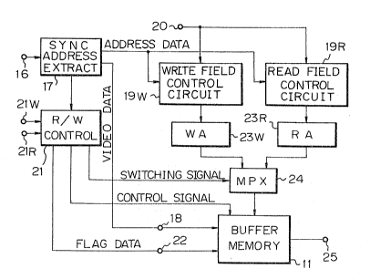
In Fig. 7, the operating system of buffer memory
11 is shown, in which the output data of inner code decoder
10 is fed in at an input terminal 16 and supplied to a sync
signal and address extracting circuit 17. As shown in Fig.
4, the sync signal and address data, which were added for
every two inner code bloc~s BI and which were again added
when the decoded data is outputted from the inner code
decoder, are separated by extracting circuit 17. The input
data from which the sync signal and address were removed is
supplied to the memory 11 through an input terminal 18. The
memory 11 has a capacity of, for example, three fields. The
separated address data is supplied to a write field control
circuit 19W and a read field control circuit l9R, and the
write field and read field in the buffer memory are
determined by the control circuits l9W and l9R,
respectively. A reproducing mode signal indicative of any
one of the standard reproducing and high-speed reproducing
, ~
--19--
13~ 2 S03l3l
modes is supplled at input terminal 20 the write and read
field control circuits.
Error correction of the data in the inner code
block BI is performed by decoder 10 and the error data with
respect to the data is formed and supplied to a read/write
(R/W) control circuit 21. A write clock is input to a
terminal 21W and a read clock is input to a terminal 21R and
both are supplied to R/W control circuit 21, which generates
control signals such as a write enable signal and the like,
to control the reading/writing operations from and into
buffer memory 11. R/W control circuit 21 also generates a
read/write (R/W) switching signal and flag data. R/W
control circuit 21 writes the flag data into buffer memory
11 through input terminal 22, and control signals, such as
the write enable signal and the like, are also supplied to
buffer memory 11. The R/W switching signal is supplied to a
multiplexer 24 for switching outputs of a write address (WA)
generating circuit 23W and a read address (RA) generating
circuit 23R. The write address or read address selected by
the multiplexer (MPX) 24 becomes the address input of buffer
memory 11. The data sequence read out of buffer memory li
is fed out at an output terminal 25.
The write address is determined on the basis of
the address data separated from the input data sequence and
when either the address data or the data is error data, for
instance, this error data is not written into buffer memory
11. The read address is such as to form the outer code
sequence and, at the same time, the deshuffling is executed
under the control of the write address or read address.
,~,~
-20-
13~12
Some examples of the constitutions of the
conversion into the outer code sequence and the address
control of buffer memory 11 or deshuffling are shown in
Figs. 8 to 10, which various embodiments of the write
address generating circuit 23W and read address generating
circuit 23R, as shown generally in Fig. 7.
The address generating circuit shown in the
embodiment of Fig. 8 controls only the read address, and the
write address (WA) generating circuit consists of a write
address (WA) counter 26W and an operaing circuit 28W. The
WA counter 26W generates the write address only the number
of times necessary for one sync block. The write address,
the address of the sync block (hereinafter, referred to as
the sync address) at terminal 29W, and the field number and
segment number data from a terminal 30W are supplied to an
operating circuit 28W. The write address is obtained from
operating circuit 28W at an output terminal 31W. When the
buffer memory 11 has sufficient memory capacity, it is
sufficient for the operating circuit 28W to merely
synthesize the input address data as the output address.
The write address serves to write the reproduced data into
the buffer memory 11 on the basis of the reproduced address
data.
The readout side is constituted by a read address
(RA) counter 26R, a read only memory (ROM) 27R, and an
operating circuit 28R. The RA counter 26R generates the
read address in the field (or frame~. ROM 27R converts the
output address of RA counter 26R into the address for the
conversion into the outer code sequence and for the
deshuffling~ The output of ROM 27R, and the read field
-21-
~ 3 ~ .`2 S03 l3 l
number data fed in at a terminal 30R, are supplied to the
operating circuit 28R. The read address ~ormed by the
operating circuit 28R is available at an output terminal
31R. It should be noted that a read only memory having a
large capacity can be substituted for the arrangement
consisting of ROM 27R and operating circuit 28R surrounded
by the broken line.
The address generating circuit shown in Fig. 9
controls only the write address. More specifically, the
output of the WA counter 26W and the sync address fed in at
terminal 29W are supplied to a ROM 27W for deshuffling. An
output of ROM 27W and the field number and segment number
data fed in at terminal 30W are supplied to operating
circuit 28W. The write address is obtained from the
operating circuit 28W and fed out at output terminal 31W.
Once again, a read only memory having a large memory
capacity could be substituted for the arrangement consisting
of ROM 27W and operating circuit 28W surrounded by the
broken line.
On the other hand, in the circuit of Fig. 9 the
readout side is composed of r~ad address counter 26R and
operating circuit 28R, which receives the output of the RA
counter 26R and the field number data fed in at terminal
30R, and generates the read address available at output
terminal 3lR.
Fig. 10 shows an address generating circuit that
controls both the write address and the read address. This
embodiment need not be explained in detail, because in the
embodiment of Fig. 9, ROM 27W is provided on the write side
and ROY 27R iS provided on the readout side. Thus, the
t
,
~ ~ 3 ~ S03131
address conversion which is executed by one ROM is
distribu1:ively executed by the ROMs 27W and 27R.
When the processing speed of buffer memory 11 is
lower than the data rate, the memory needs to be made
operative in parallel. Flg. 11 shows an arrangement of
buffer memory 11 suitable for performing parallel
operations, in which memory 11 is divided into N parallel
channels. More specifically, buffer memory 11 i5 divided
into N parallel channels comprised of N memory chips 111',
to llN' and N address generating circuits 231' to 23~' are
provided for the memory chips 111' to llN', respectively.
The memory control signals, such as the write enable signal
and the like, are supplied in common from an input terminal
32 to memory chips 111' to llN'.
The respective input data of memory chips 111' to
llN' are supplied from a serial ~-~parallel (SPS) converter
33. The SPS converter 33 is controlled by a control circuit
34 and converts the reproduced serial data fed in at
terminal 18 into paralleI data, thereby reducing the data
rate to 1/N. The respective output data of the memory chips
111' to llN' are supplied back to SPS converter 33, wherein
they are converted back into the serial data. Thus, the
deshuffled output data which was converted into the outer
code sequence is made available at the output terminal 25.
In the case of handling color video data, it is
generally necessary to use a buffer memory having a
parallel processor circuit arrangement, as shown in Fig. 11,
in terms of the data rate, however, the parallel
constitution glenerally needs a plurality of address
generating circuits 231' to 23NI~ so that the control of
SO31~i
~ 3 '1 ~
these address generating circuits becomes complicated. The
problems which are caused when such a constitution for the
parallel operations of the memory is used, and the methods
that can solve the problems, are described hereinbelow.
In order to aid the understanding of the shuffling
and deshuffling operations, an explanation is set forth with
reference to Fig. 12, with regard to how the data is input
into and read out from the buffer memory of shuffling
circuit 4 during the recording operation.
The 4800 sample groups that are recorded by one
rotary head are shown in Fig. 12 in accordance with the
input sequence. In one sample group, as represented in
three-dimensions in Fig. 12, one luminance data Yl is
arranged at the lowermost front position, and the color
difference data U and V and the other luminance data Y2 are
sequentially arranged proceeding in the depth direction.
Alternatively, these data can be arranged in accordance with
the sequence U, Yl, V, anZ Y2.
In Fig. 12, the data is sequentially written into
the buffer memory as indicated by the arrows from the start
point ST which coincides with the sampling data at the left
end at the frontmost position of the first sample group.
More specifically, the data is sequentially written into the
buffer memory from the first sample group, the second sample
group, the third sample group, ..., until the data of the
last 4800th sample group is flnally written into the buffer
memory. Upon completing the writing operation into the
buffer memory, the shuffling operation may be also executed
with respect to the direction of the outer code sequence.
-24-
~ 2 SO3131
The reading operation of the data from the buffer
memory of the shuffling circuit 4 is described with
reference to Fig. 13, because it is in this reading
operation that the shuffling process is carried out.
Fig. 13 shows the recording sequence of the input
data, in which ( ~= 1, 2, ..., 150) indicates the numbers of
the columns for every four outer code blocks with regard to
Y1, U, V, and Y2. The number added for each sample group
denotes the number I of the inner code block into which the
sample group is written. In the shuffling process, 150
sample groups located along every line in Fig. 13 are
rearranged to form ten inner code blocks, each consisting of
fifteen sample groups. The shuffling process based on the
same rule is performed with respect to each row and, from
the sampling data shown in Fig. 12, a total of 320 inner
code blocks BI of (I = 1 to 320) are formed, as shown in
Fig. 3.
In this shuffling process, with respect to~ , a
total of fifteen sample groups, which are arranged at
regular intervals of every ten sample groups from the oth
sample group as the start sample group, are selected.
Namely, the oth, (o + lO)th, (o + 20~th, (o +30)th, ---, (o
+ 130)th, and (o + 140)th sample groups are selected. The
selected sample groups are supplied to inner code encoder 5
and one inner code block is formed. For instance, with
respect to the first sample group, the sample groups of the
numbers (o = lr 6, 2, 7, 3, 8, 4, 9, 5, 10) with regard to
the number 1 beaome the respective first sample groups of (I
= 1 to 10) of the inner code blocks.
-25-
~3~ 2 SO3131
The data is recorded in accordance with the
sequence from (I = 1) of the inner code block to (I = 2), (I
= 3), ..., (I = 320) and every adjacent two blocks
constitute the sync block, and the data of (4 x 15 x 2 = 120
samples) is included in the sync block. In Fig. 13, the
example in which one outer code block BO was separated is
illustrated. As shown in this e~ample, the outer code block
BO is formed for every 32 samples arranged in the vertical
direction.
Fig. 14 shows the data arrangement in Fig. 13 with
regard to rotary head A, and the data arrangements of the
other three rotary heads B, C, and D are similar to that of
Fig. 13, therefore, they axe not shown therein. In Fig. 14,
the numbers o of the first sample groups indicating the
reading sequence as the inner code block are shown in the
lateral direction. More specifically, Fig. 14 shows the
composition of the data arranged in accordance with the
sequence of the inner code block numbers, that is, the
sequence as it appears after completion of the shuffling
process. The d~ta of 4800 sample groups included in the
data arrangement is recorded in accordance with the sequence
of [(Yl~~U ~ V~ Y2) of each of fifteen sample groups of (I =
1)-3[(Yl-3U~V-~Y2) of each of fifteen sample groups of (I =
2)], A pair of rotary heads A and B and a pair of rotary
heads C and D record the parallel data, respectively.
Fig. 15 shows an enlarged diagram of the portion
surrounded by the heavy solid line on the leftmost side in
Fig. 14, which shows the portion in which a total of
thirt~-two inner code blocks of (I = 1, 11, 21 ---, 311)
were piled. In Fig. 15, the sampling data of the inner code
,~
-26-
13~ 2 S03131
block of ~I = 1) is reccrded in accordance with the sequence
indicated by the arrows.
In buffer memory 11 of the reproducing circuit, a
deshuffling process opposite to the shuffling process is
executed each time the reproduced data is output from each
rotary head. When buffer memory 11 has the parallel
processing embodiment using the SPS converter 33, as shown
in Fig. 11, the data cannot be simultaneously read out in
parallel from the same memory chip. Therefore, if the data
is not distributed into the respective memory chips upon
writing, there will be caused an inconvenience such that the
inner code sequence cannot be converted into the outer code
sequence. The writing process in the embodiment where the
parallel number N of buffer memory 11 is six will be
described hereinbelow.
The writing operation into six memory chips is
carried out in principle in accordance with the data
reproducing sequence based on the inner code block numbers
I, that is, the numbers r in Fig. 16, however, because the
sampling data equal to the integer times the number of
memory chips is included in the inner code block, if the
reprod~ced data is merely converted into the parallel data
on a six-sample unit basis and written into the six memory
chips, the number of chips into which the head sampling data
Yl of each inner code block is written will always be 1. In
addition, the data of the same chip number is lncluded in
the vertical direction as well, thus, the deshuffling
process cannot be performed.
To prevent this, as represented in Fig. 16, the
sampling data of the blcck number (I = 1) is sequentially
~3~ .2 S03131
distributed into six memory chips and in the case where the
data of the next lnner code block is written, two chip
numbers are skipped and the chip number of the sampling data
of the head luminance data Y1 of the inner code bloc~ of (I
= 2) is set to 3. In a manner similar to the above, the
above control procedure is likewise executed with respect to
the inner code blocks of (I - 1 to 10) of the first row.
With regard to the inner code block of (I = 11 to 20) of the
second row, the chip number of the sampling data of the head
luminance data Y1 of the inner similar to the above is also
performed with respect to the inner code blocks of (I = 12
and subsequent numbers).
The chip numbers of the head sampling data of Y1
of the inner code blocks, which are arranged at the leftmost
positions of the 3rd, 4th, ..., 32nd rows, are set so as to
have the cyclic numbers of the sequence of (1, 2, 3, ....
6). In other words, when the data is written into each
memory chip of buffer memory 11, one chip number is skipped
in response to the change to the next row.
Fig. 17 shows a set of thirty-two inner code
blocks on the leftmost slde in Fig. 16 as a unit of the
sample group. As will be understood from FigsO 16 and 17,
because each column in the vertical direction is constituted
by a set of chip numbers of (1, ~, 3, ..., 6), when the data
is read out in the vertical direction, namely, by the outer
code sequence, it is possible to avoid the impossible
operation to simultaneously write in and read out the data
from the same memory chip.
The data is read out from six memory chips in
accordance with the outer code sequence, more specifically,
the data is read out in the vertical direction, in refexence
-28-
.
.
S03131
to Figs. 16 and 17. In Fig. 16, r indicates the writing
sequence of the unit of the inner code block and o
represents the reading sequence of the unit of the inner
code block.
The reading sequence regarding the chip numbers
will be more practically explained with reference to Figs.
18 and 19, in which Fig. 18 shows a part of the sampling
data which is included in the first row of the data
arrangements of Figs. 16 an 17 and is read out first.
A set of data of (r = 1, o = l, ~ ~ l) in Fig. 18
corresponds to a two~dimensional diagram showing the data
blocks of one column (I = l) at the leftmost position of the
set of data in Fig. 17. The next set of data of ~r = 3, o =
2, ~ =2) is a two-dimensional diagram showing the data
blocks of one column (I = 2) at the leftmost position of the
relevant data block in Fig. 16. Likewise, a set of data of
(r = 5, o = 3, ~ =3) and a set of data of (r = 7, o = 4,
~=4) are shown in Fig. 18.
In the reading operation, every six samples of the
chip numbers 1 to 6 in the vertical direction are read out
in parallel from the six memory chips. In this case, as
respectively shown in Figs. 16, 17, and 18, after thirty-two
sampling data were read out in the vertical direction, the
chip number of the sampling data of the 32nd memory chip and
three continuous dummy sampling data are added. Therefore,
when the reading operation is shifted from the set of data
of (r = 1, o = 1~ ~ =1) to the set of data of (r = 3, o = 2,
~2) due to the address control for deshuffling, the color
difference data U is read out of memory chip number 6, as
indicated by the arrows in Fig. 19, because the dummy
sampling data of the ch1p numbers (3, 4, 5)~ exists.
q
,
. .
,
1 3 ~ 2 SG ~ 1 3 1
Next, when -the color difference data U and dummy
sampling data are read out in the vertical direction, the
luminance data Yl of the memory chip number 5 in the set of
the same data is read out, because the dummy sampiing data
of the memory chip numbers (2, 3, 4) exists. Whe~ the
luminance data Yl and dummy sampling data are read out in
the vertical direction, the luminance data Y2 of the chip
number 4 of the set of data of (r = 1, o ~ =1) is read
out. Subsequently, the data is similarly read out in
accordance with the sequence ind:icated by the arrows in Fig.
19. When the luminance data Y2 of the set of data of (r =
3, o = 2, ~ =2) and the dummy sampling data of the chip
numbers (4, 5, 6) are read out in the vertical direction,
all three data sets of (r = 1, o = 1, =1), (r = 3, o = 2,
~2), and (r = 5, o = 3,~ =3) are completely read out. The
data of one horizontal interval lH is read out in accordance
with the sequence shown in Fig. 19, so as to coincide with
the inherent sequence of the digital color video signal as
accurately as possible within lH, however, as the reading
sequence of three data sets, various modifications other
than that shown in Fig. 19 are also possible.
The sum of those -three data sets is the data (30 x
4 x 3 = 360 samples) of lH which is recorded/reproduced by
one rotary head. In the case of a unit of lH, the read data
is obtained on the basis of the sequence that is coincident
with the seyuence of the digital color video signal due to
the foregoing reading operation. The inherent sequence of
the digital color video signal within lH is (Yl~U-~V-~Y2)
for every set of data. Therefore, the data of six samples
read out in parallel from the respective memory chips is
_~n-
13~ SG3131
converted into the serial data by the serial~ ~parallel
converter and thereafter converted into the data having the
inherer~t sequence of the data within lH by a memory having a
relatively small capacity. secause the dummy sampling data
is unnecessary, it is not used in the output of this small
capacity memory.
secause the reading operation based on the
sequences of Figs. 18 and 19 is executed for every three
data sets of lH, in the case of the data set of (r = 10, o =
1O, Q = 1O), one set is constituted by this set and two data
sets of (r = 1, o = 1, ~=1) and (r = 3, o = 2, e= 12). In
such case, the process similar to the above is applied.
By adding three dummy sampling data in the
foregoing deshuffling process, data which was deshuffled in
accordance with a sequence that is extremely similar to the
inherent sequence of the digital coior video signal can be
obtained.
Even more detailed embodiments of buffer memory 11
are described with reference to Figs. 20A and 20B, which
show the circuits in which a dynamic RAM is used as the
buffer memory 11.
First, referring to Fig. ~OA, the input data is
supplied through eight serial-to-parallel (S/P) converters
33A " 33B " ' 33H' to a buffer memory lla to store the
digital video signal. The output data of the buffer memory
lla is taken out through eight parallel-to-serial (P/S)
converters 33A"' 33B"' ' 33H"-
The input data consists of eight parallel bits ofone sampling data and is sequentially supplied, one bit by
one bit starting at the most significant bit, to the S/P
-31~
- S03131
~L 3 ~ 2
converters 33A' to 33H' through input terminal 18. The data
of fifteen parallel bits is formed for every corresponding
number of bits of the same sequence, and the output data of
fifteen parallel bits of the buffer memory lla is converted
back into serial data by P/S converters 33A" to 33H"'
respectively. Thus, the output data of eight parallel bits
is obtalned from the output terminal 25 of memory lla.
The error flag of one bit from the inner code
decoder 10 is supplied at input terminal 22 through a latch
circuit 35 to a flag memory llb to store the error data.
The error flag read out of the flag memory llb is taken out
at an output terminal 37 through a latch circuit 36 and
supplied to outer code decoder 12 together with the data
read out of buffer memory lla from terminal 25.
The write clock fed in at terminal 38W and the
read clock fed in at terminal 38R are supplied to a memory
control circuit 38. Further, the reproducing mode signal
fed in at terminal 19 is fed to memory control circuit 38.
The reproducing mode signal becomes, for example, a high
level in the ordinary reproducing mode in which the tape
speed upon recording is equal to the tape speed upon
reproduction and, in the slow motion reproducing mode, in
which the tape speed upon reproduction is slower than the
tape speed upon recording. On the contrary, the reproducing
mode signal becomes, for instance, a low level in the case
where the tape speed upon reproduction is faster than the
tape speed upon recording.
~ emory control circuit 38 generates address data
(ADD), a row address strobe signal (RAS), and a column
address strobe signal (CAS), which are common to the buffer
-32-
~3~ 2 SO3131
memory lla and flag memory llb. The memory control circuit
38 also generates a write enable signal WE for buffer memor~
lla, a write enable signal A~E for flag memory llb, and a
latch pulse. The write clock is synchronized with the input
data and is formed from a reference clock. Therefore, the
time base variation component is removed by buffer memory
lla~
Although not specifically shown in Fig. 20A, the
reproduction address for every sync block BS is supplied to
memory control circuit 3~ and the write address is
determined on the basis of this reproduction address.
Memory control circuit 38 controls one or both of the write
address and read address, thereby executing the conversion
from the inner code sequence into the outer code se~uence
and the deshuffling, and such address control is commonly
performed for the buffer memory lla and flag memory llb.
Thus, each sampling data and error flag of the output data
are synchronized with each other.
Fiq. 20B shows a buffer memory system representing
another embodiment of buffer memory 11, in which the same
parts and components as those shown in the buffer memory 11
of Fig. 20A are designated by the same reference numerals
and their descriptions are omitted. Referring to Fig. 20B,
a first flag memory llb and a second flag memory llc are
provided to store error data as the flag memories. The
one-bit error flag from latch circuit 35 is supplied to
first flag memoxy llb, and the error flag read out of the
flag memory llb is supplied to a latch circuit 36b through a
selector 36a. The N/O flag is supplied form memory control
circuit 38 to latch circuit 35. The error flag fed out at
-33~
~ 3 ~ .2 So3131
output terminal 37 from latch circuit 36b is supplied to the
outer code decoder 12 together with the data read out of
buffer memory lla. The error flag read out of second flag
memory llc is supplied as the other input of the selector
36a. In this embodlment, a field identifying signal fed in
at terminal 19 is fed to memory control circuit 38, and this
field identifying signal consists of a reference field
identifying signal on the readout side of buffer memory lla
and a reproduced field identifying signal based on the field
address separated from the reproduced data. When the
operation is shifted to the nsxt field by the reference
field identifying signal, selector 36a selects the error
flag which is read out of second flag memory llc in place of
the error flag, which is read out of first flag memory llb.
When the reproduced field identifying signal
instructs a shift to the different field during one scan of
rotary heads 7. selector 36a selects the error flag, which
is read out of first flag memory llb, in place of th~ error
flag, which is read out of second flag memory llc.
Therefore, in the slow-motion reproducing mode, in the first
field, the error flag read out of flag memory llb is
selected by selector 36a. Next, the error flag read out of
flag memory llc is selected by selector 36a for the period
when the data of the same field is reproduced.
On the other hand, in the standard reproducing
mode, after an expiration of one field period, the
reproduced data of the next different field is generated, so
that the error flag which is read out of first flag memory
llb is always selected. Further, in the high-speed
reproducing mode, the data of a different field is
-34-
2 S03l3l
reproduced by one scan, so that the error ~lag which is read
out of first flag memory llb is also always selected. The
error flag selected by selector 36a is supplied to latch
circuit 36b and second flag memory llc.
Memory control circuit 38 generates the address
data (ADD), row address strobe signal (RAS), and column
address strobe signal (CAS), which are common to buffer
memory lla and flag memories llb and llc. Memory control
circuit 38 also generates the write enable signal WE of
buffer memory lla, the write enable signal AWE of flag
memories llb and llc, and the latch pulse.
The operations of the buffer memories of Figs. 20A
and 20B are described with reference to Fig. 21, in which A
represents a timing signal used to specify the read cycle
(R) and write cycle (W). Waveform B shows the timing of the
addresses ADD that are supplied to the buffer memory lla and
flag memories llb and llc. In that regard, the column
address is first set and the row address is then set, and
waveform C shows the row address strobe signal RAS and
waveform D shows the column address strobe signal CAS.
Buffer memory lla performs the reading operation
when the addresses ADD are specified, the address strobe
signals RAS and CAS are sequentially set to a low level, the
column address and row address are sequentially read, and
the write enable signal WE goes to a high level. Buffer
memory lla executes the writing operation when the address
strobe signals RAS and CAS are sequentially set to a low
level, the addresses are read, and the write enable signal
WE goes to a low level. Although the writing and reading
operations of flag memories llb and llc are also executed in
-35-
,
, .
- . . . .
2 S03131
a manner similar to the above, they are controlled by
another write enable signal AWE different from that of
buffer memory lla.
Waveforms E and F of Fig. ~1 show examples of the
write enable signals WE and AWE in the ordinary reproducing
mode, respectively, present in the embodiment of Fig. 20A.
The write enable signal WE shown in waveform E always goes
to a low level in the write cycle. Therefore, the input
reproduced data is sequentially w:citten into buffer memory
lla.
In waveform as shown at reference numerals 39a and
40a, the write enable signal AWE of flag memory lla goes to
a low level immediately after the error flag of the
designated address was read out. Then the error flag
representing that the error exists in this designated
address i9 written. If the data that is written into buffer
memory lla for interval 39b when the write enable signal WE
is at a low level has no error, the error flag indicative of
no error is written into flag mèmory lla for an interval 39c
when the write enable signal AWE is at a low level, then the
error flag is rewritten.
On the other hand, if the data which is written
into buffer memory lla for an interval 40b has errors, the
write enable signal AWE is held at a high level for an
interval 40c and the error flag is not rewritten. In this
manner, in the ordinary reproducing mode, as well as in the
slow-motion reproducing mode in which the data of the outer
code block BO is reproduced for a few fields, both the data
from the inner code decoder 10 and the error flag are
written into buffer memory lla and flag memory llb.
-36-
.2 S03l3l
In Fig. 21 waveforms G and H show examples of the
write enable signals WE and AWE in the high-speed
reproducing mode, respectively. In a manner similar to the
case in the ordinary reproducing mode and slow-motion
reproducing mode, in the high-speed reproducing mode the
error flag is written into flag memory llb after the data
was read out of buffer memory lla, so that it is indicated
that the data of that address was previously reproduced. In
addition, the error data is not writ~en into buffar memory
lla, but the data having no error is written into buffer
memory lla, the error flag indicative of no error is written
into flag memory llb, and the error flag is rewritten. The
data and error flags respectively read out of buffer memory
lla and flag memory llb are not subjected to the error
correcting process by outer code decoder 12 but are directly
supplied to the error concealment circuit 13, by which the
error concealmant is executed.
In the embodiment of Fig. 20B, the ~rite enable
signal WE shown in waveform E of Fig. 21 goes to a low level
in the write cycle in the case of data having no error.
Therefore, the input reproducPd data having no error is
written into buffer memory lla. As shown in waveform F, the
write enable signal AWE of flag memories llb and llc is set
at a low level immediately after the error flag of the
designated address was read out. The error flag
representing the presance of the errors is written into the
designated address of flag memory llb through latch circuit
35, and the error flag read out of flag memory llb through
selector 36a is written into the other flag memory llc.
Therefore, the error flag of flag memory llb is copied into
37-
.
3 ~ S03 1 3 1
flag memory llc. In the case where the data that is written
into buffer memory lla for the low-level interval has no
error, the error flag i.ndicative of the absence of error is
written into flag memory llb fGr the interval when the write
enable signal AWE in the write cycle is at a low level, and
the error flag is rewritten.
In the slow-motion reproducing mode, selector 36A
selects the output of flag memory llc upon reading of the
same field at the second and subsequent times. Thus, the
error flag copied into flag memory llc is repeatedly
outputted for every field.
Assuming that the memories of the fields provided
in buffer memories lla are denoted as FM1, FM2, and FM3,
respectively, when the tracks T1 and T2 in Fig. 5 are
scanned, the reproduced data of the preceding field Fo which
was reproduced by the former half part of the scan is
written into the field memory FM3, and the reproduced data
of the next field Fl, which was reproduced by the latter
half part of the scan, is written into the field memory FM1. -
For the interval from the last half parts of the tracks T
and T2 to the first half parts of the tracks T11 and T12,
the reproduced data of the field F1 is written into the
field memory FM1 and at the same time, the data of the field
Fo is read out of the field memory FM3. For the interval
after the last half parts of the tracks T11 and T12, the
reproduced data of the field F2 is written into the field
memory FM2 and at the same time, the data of the field F1 is
read out of the field memory FMl. In a manner similar to
the above, the above operation is repeated.
_ ~ Q._
~3~ 2 S03131
In the slow-motion reproducing mode in which the
speed of the magnetic tape is, for exampla, 1/2 of the
recording speed, it takes a tlme that is twice as long as in
the standard reproducing mode in order to reproduce the data
of the field Fl. Therefore, for the interval of those two
fields, the data of the preceding field Fo stored in the
field memory FM3 is repeatedly read out. The selector 36a
selects the error flag read out of flag memory llb in the
first reading operation of the data of the field Fo ~rom the
field memory FM3. In the next second reading operation,
selector 36a selects the error flag read out of flag memory
llc and, because the field of the reproduced data changes
upon scanning of the tracks T11 and T12, selector 36a
selects the error flag from flag memory llb.
The present invention is not limited to a digital
VTR of an individual component system, but may be also
applied to the digital VTR of the composite system, as well
as to other apparatus using other similar error correction
code techniques.
The invention can be also applied to an apparatus
for decoding error correction code, which constitutes the
code sequence in the oblique direction of a two-dimensional
arrangement of the data. The error correction code is not
limited to the Reed-Solomon code but various other kinds of
correction codes, such as b-adjacent code, BCH code, which
are conventionally known may also be used.
According to the present invention, by providing a
memory to rearrange the inner code sequence i.nto the outer
code sequence between the decoder of the inner code and the
decoder of the outer code, it is possible to execute the
_~a _
'' '~: ' ' ' ':
,
~ . '
~ 3 ^~ S~3131
rearranging process using a memory of capacity only as large
as is necessary to recover the video data in the variable
speed reproducing mode. Therefore, there is no need to
provide a memory for use only in the data rearrangement,
with the result that the memory scale can be reduced and the
number of peripheral circuits of the memory can be
decreased.
In addition, according to this invention, by use
of the memory of a large capac:ity necessary to recover the
video data in the variable speed reproducing mode, there is
no need to provide a memory for use only in the deshufflinq
process. Thus, the necessary capacity of the memory and the
number of peripheral circuits of the memory can be also
reduced.
Further, according to the invention, in the case
where the data of one field is obtained due to the scanning
operations of a plurality of times by the rotary heads, as
in the slow motion reproducing mode, the error correction
can be executed using the outer code, so that a good
reproduced picture quality can be obtained.
In the case of providing a plurality of memory
chips in paxallel in the memory to solve the drawback in
which the processing speed of the memory is slow, by
providing a predetermined number of dummy data upon either
one or both of the writing and reading operations, the
simultaneous access of the same memory chip can be
prevented.
In addition, according to this invention, by
writing the error data into the buffer memory in the
ordinary rsproducing mode and the slow-motion reproducing
n.
'
' : ' -
.
~3~ L`~ aC~
mode, this error data can be corrected by the outer code
decoder at the next stage. In th s way, the error
correcting capability can be improved.
According to this invention, when the reproduced
data is read out or the buffer memory, the flag is read out
together with the data and the next flag that is read out
immediately after that is changed to the flag indicating
that the readout reproduced data is the preceding reproduced
data. Therefore, it is possible to prevent deterioration of
the reproduced image due to a mixture of the preceding
reproducted data. On the other hand, according to the
invention, the readout flag is written into the second flag
memory and the auxiliary flag from the second flag memory is
used as the flag when the data of the same field is read out
two or more times. Thu.s, it is possible to prevent the
problem such that all of the flags of the data read out at
the second subsequent times indicate the preceding
reproduced data.
The above description is presented on preferred
embodiments of the invention, but it will be apparent that
many modifications and variations could be effected by one
skilled in the art without departing from the spirit and
scope of the novel concepts of the invention, which should
only be determined by the appended claims.
-41-
,