Note: Descriptions are shown in the official language in which they were submitted.
3~
-- 1 --
Patent
MICROPROCESSOR BASED INTEGRATED
GENERATOR SET CONTROLLER APPARATUS AND METHOD
s Field of the Invention
This invention relates generally to a control process
system, and more particularly to an improved method and
apparatus for controlling an electrical generator.
Backaround o the Invention
The present invention relates to a microprocessor
based, highly integrated generator set controller. More
particularly, the present invention relates to an
electrical generator set and power system controller
capable of sharing real and reactive power with parallel
generator sets and further providing for precisè frequency,
voltage and current regulation while utilizing a single
processorO ~y so doing, system performance, reliability,
and cost are optimized.
The output voltage of an electrical generator is
determined by the excitation of the field~windings of the
generator. Therefore, the output voltage of the generator
may be controlled in a closed~loop ashion by monitoring
its output voltage, comparing that voltage to a reference
voltage level, and generating an appropriate signal to the
field winding. ~he speed of the engine driving the
generator controls the generator output waveform frequency.
Thereore, the frequency of the output waveform may be
controlled in a closed-loop fashion by monitoring the
revolutions of the engine, co~.paring the revolutions to a
reference and generating an appropriate signal to adjust
the engine throttle.
Analog controller systems are widely used in the
control of electrical generators. This type of controller
typically employs distinct components to independently
control the two closed-loop control functions (i.e., the
output voltage of the electrical generator and the
~L3~322~
-- 2 --
frequency of the output voltage waveform of the electrical
generator). They typically do so without sharing
information concerning the status of the other closed-loop
control function. Further, the circuitry providing for
these two control functions are not interconnected to one
another. Therefore, in an analog system, not only are the
components discrete, but the two control systems are both
independent and discrete from one another.
Due to their dual discrete design, analog systems also
have the disadvantage of requiring duplicate input
transformers and circuitry when additional features are
added. Also, since the systems are analog, they cannot
perform self-diagnostics, indicate their operational state
or integrate their control processes to optimize
performance. Finally, the discrete controls require
calibration for each electrical generator production unit.
There have been attempts to integrate generator set
controllers, for example Mezera et al, U.S. Pat. No.
4,322,630, and provide for microprocessor control of the
control functions. However, none of the attempts have
fully integrated the entire generator set control function.
Further, none have integrated the precise regulation of
frequency, voltage, and current conditions, automatic
synchronization of parallel generators, permissive
paralleling, and both real and reactive load sharing
control during parallel operation. The present invention
provides an integrated system and method which provides
increased ~erformance over the above described generator
set controllers.
Summary of the Invention
The present invention relates to a highly integrated
control system for the monitoring an~ control of an
electrical generator set which hereafter will be referred
to as a gen-set for convenience. More specifically, the
present invention provides the capability for implementing
~l3~L322~
~ 3 --
the followin~ control functions: electronic governor
control, automatic voltage regulation, regulated short
circuit current, engine speed sensing, engine fault
monitor, circuit interrupter control, overload fault, short
circuit fault, automatic synchronization, permissive
paralleliny, over and under voltage faultsr remote metering
and control, starting aid control, output power calculation
and display, reverse power fault, permissive paralleling
control, real power load sharing control during parallel
1~ operation, reactive power load sharing control during
parallel operation, built-in self-diagnostics, and
provision for external diagnostics equipmentO
The control system includes a microprocessor control
unit comprising a central processing unit tCPU), several
high speed input-output devices, an eight channel analog to
digital converter, an erasable programmable read only
memory (EPROM), a pulse width modulator (PWM), an interrupt
control, input/output (I/O) expander chips and a serial
port. By way of example, parameters monitored by the
control unit include engine speed, generator voltage and
current, load bus voltage, engine oil pressure, water
temperature, fuel and speed, addltional parallel gen-sets,
and operator input. By monitoring these signals~ comparing
the signals to reference levels, and determining the
appropriate output according to control equations, the
microprocessor controls the operation and output of the
engine generator system.
The two main control functions of the integrated
controller are the regulation of the engine's revolutions
per unit time, which affects the frequency of the generator
output waveform, and the regulation of the excitation of
the field windings of the generator, which affects the
output voltage of the generator. To control these two
functions, the microprocessor utilizes two different
proportional, integral, derivative control equations which
will be referred to herein as PID equations for
convenience. The general form of a ~ID equation in the
,
,'~ ~, '
~31~22~
-- 4
time domain is as follows:
~(t) = Kp E(t) + Ki ~ E(t) dt + KD d(t~
where Kp, Ki and KD are the respective constants for the
proportional, integral and derivative terms respectively.
The constants for the preferred embodiment of the present
system control were derived from the analog compensation
networks previously utilized with the gen-set. However t
the constants may be derived by determination of the
transfer function from the steady-state response or other
such methods as are well known in the art. The previous
analog compensation network from which the current
constants were derived is further described in U.S. Pat.
No. 4,533,863.
To convert analog compensation networks to equations
which may be utilized by a digital microprocessor, the time
domain equations describing the system are converted to the
Z-domain using a bilineal transform. The resulting
equations are factored and used by the microprocessor as
control equations. A thorough discussion of digital
control using microprocessors may be found generally in P.
Katz, Diqital Control Usinq Microprocessors, ~1981
Prentice/Hall).
To derive the actual PID control equations for the
preferred embodiment from the existing analog compensation
network, three steps are performed. First, the transfer
function of the analog compensation network is determined.
Second, the transfer function is converted to the Z-domain
u~ing the bilineal transform:
S = 2 ~Z-l)
T (Z+i)
Finally, the resulting equation is converted to a numerical
algorithm. To perform this final step, the Z-domain
equation may be factored to the following form:
:
. .
` ` :iL3~ 2~
~ lZ l) ~1 +~2Z l)
D(Z) = -1 1
(1 + ~Z ) (1 + ~3Z
This equation's coefficients may be shown to
correspond to a cascade realization, as is well known in
the art (see e.g., Katz at 140, infra). By then defining
four constants (Kl, K2, K3 and K4) whose values are based
on the resistors and capacitors of the analog system, and
allcwing six varlables to be established (Al, Bl, Cl, Dl,
Xl and X2) to store the intermediate results required by
the algorithm, one may then express the control process
algorithm as follows:
if, A = (Kl) (Vl)
B = (K2) (Xl)
C = (K3) (X2)
D (K4) ( 2)
then,
Xl = Xl + A
X2 = A + B + C
Ul = A ~ B - D
Where Ul is the output of the algorithm and Vl is the
input.
This procedure is similarly utilized to obtain each of
the control equations for the gen-set system. The
resulting two PID control equations being identical in
form, but utilizing different numerical values for the
coefficients. To obtain the numerical values for the
voltage regulation PID coefficients durins current
regulation, quantitative testing was performed to determine
best results.
The integrated controller unit includes data
processing means for computing sampling rates and values of
the various monitored parameters, for solving the control
equations, and for comparing the monitored parameters
~ - 6 - ~3132~
against fixed values to determine if the measured
parameters have exc~eded their rated values. The data
processing means further include means for comparing the
frequency and phase of the main bus voltage and the gen-
S set's frequency and phase. Fault displays, meters, andserial communication links are also provided. A more
complete discussion of the microprocessor used in the
preferred embodiment of the present invention may be found
in the Intel, Embedded Controller Handbook (1988)(copyright
1987).
Briefly, in operation, a preferred embodiment of the
integrated control unit constructed according to the
principles of the present invention, samples a regulated
phase voltage every two milliseconds. Each one-half
millisecond between the two millisecond sample, the control
unit samples one of several other analog channels. These
channels include the two voltage phases of the generator
which are not regulated, the three phase currents of the
generator, the phase angles of the voltages and currents
produced by the generator, and several other system
parameters. ~he microprocessor utilizes the sample by
applying the control process equations, and transmitting an
appropriate regulated voltage response signal through a
pulse width modulator, resident in the microprocessor, to
excite the field windings of the generator.
The frequency of the generator is similarly regulated
by the control unit. The monitoring of the frequency is
interrupt driven, is asynchronous and occurs after
receiving a set number of pulses from a magnetic pickup
located on the engine driving the generator. The
microprocessor utilizes the sampled engine speed by
applying the appropriate control system equation, and
transmitting an appropriate signal through a high speed
input-output device ~resident in the microprocessor) to the
governor output stage which controls the engine throttle.
In this m,nner, the generator voltage and frequency of the
electric gen-set is controlled by the microprocessor.
. ,~ .. ~.j
,~
:.,
,.
~3~312~
.
Besides integrating the basic gen-set control
functions, another feature of the present invention is its
ability to switch to a current regulation mode in real time
(on-the-fly) during fault conditions. The microprocessor
switches from voltage to current regulation whenever the
current being drawn from any of the three phases of the
gen-set exceeds 300% of the rated current of the generator.
During this mode of regulation, the microprocessor changes
the voltage regulation PID equation coefficients in order
to provide for a better system response, while limiting the
output current. The system provides the current regulation
on the phase exhibiting the largest output current. This
provides for regulating one phase which may have larger
loads connected to it than the other phases. During
current limiting regulation, the analog channel sampling
technique is changed to sample the largest current every
two milliseconds, with the other channels being sampled at
one-half millisecond intervals as previously described.
Another feature of the present invention is its
ability to synchronize the gen-set with the load bus. To
synchronize the gen-set~ the microprocessor monitors one
phase of the load bus voltage. This signal is converted
into a square wave by a zero crossing detector and compared
to a similar signal generated by a second zero crossing
detector whose input is one phase of the gen-set voltage.
The comparison is provided by two monostable devices.
These devices generate a voltage corresponding to the phase
difference between the two voltages. The voltage is then
processed by a proportional-integral compensator circuit to
provide a signal used by the microprocessor in its governor
regulation module to adjust the gen-set frequency to
synchronize the gen-set with the bus.
Still another feature of the present invention is the
capability to share the load present on the load bus with
other gen-sets connected to the bus. When gen-sets are
hooked in parallel to a load bus, optimum performance is
achieved by providing that each gen-set equally share the
' ', ~ '
~31~22~
real and reactive power drawn by that load. Therefore,
provision is made for the controller to calculate the real
and reactive power delivered by the gen-set to the load bus
from each of the three phases and provide output signals
corresponding to the real and reactive power delivered
respectively~ Other generators in parallel with the load
bus also provide similar signals. The signals are compared
in an analog manner and correction signals provided back to
the controller for both real and reactive power. The
correction signals allow the controller to adjust the
regulation of the engine to balance real power and adjust
the regulation of the field winding excitation to balance
reactive power.
Another feature provided is a microprocessor
controlled trip curve for both overload and short circuit
conditions. These conditions are based on the
characteristics of the generator and in part on government
specifications. This feature is provided by controlling
the circuit interrupter. The interrupter is opened at a
given time associated with the amount of current being
drawn by the load. When the interrupter is opened, the
gen-set is isolated from the load bus thereby removing the
overload or short circuit condition.
A further feature is provided to allow for permissive
paralleling of gen-sets. This feature provides that the
gen-set contactor will not be allowed to close unless the
load bus is not energized or two conditions are met for a
specific time interval. In a preferred embodiment, first
condîtion is that the phase difference between the gen-set
output waveform and the load bus is less than ~0 degrees
Iplus or minus). The second condition is that the voltage
difference is less than 8 volts (plus or minus). The
re~uirement that these two conditions be satisfied for a
specific time interval avoids allowing the contactor to be
closed when the conditions have been met only
instantaneously.
An additional feature provides for a reduced gen-set
,. ,,;,~ ;' ~.~ '
., , .:
~ : :': '
~ :' : ~; ' '~
3~
engine speed upon start up. The feature is a "soft start"
provision which allows the gen-set to increase its speed
from zero revolutions per second up to its normal operative
speed over several seconds. There is also provision for a
voltaye soft start, whereby the exitation of the field
windings is limited to provide for an increase of the
generator output voltage from zero volts to its normal
operative value over several seconds.
The invention also has a voltage load provision,
whereby if a heavy load is placed suddenly on the load bus
(e.g., when a large electric motor is started) thereby
slowing the gen-set engine, then the gen-set voltage is
allowed to drop proportionally to the reduction in speed of
the gen-set engine. The drop in voltage reduces the load
on the engine allowing the frequency to recover to the
reference value.
In addition to other features and advanta~es, the
present invention provides a system to control the gen-set,
while sensing and protecting from over and under voltage or
current fault conditions, and sharing real and reactive
loads with additional gen-sets. These and various other
advantages and features of novelty which characterize the
present invention are pointed out with particularity in the
claims annexed hereto and form a further part hereo~.
However, for a better understanding of the invention, its
advantages and objectives obtained by its use, reference
should be made to the Drawing which form a further part
hereof, and to the accompanying descriptive matter, in
which there is illustrated and described a preferred
embodiment of the present invention.
Brief Description of the Drawin~
In the Drawing, wherein like reference numerals and
letters indicate corresponding elements throughout the
several views:
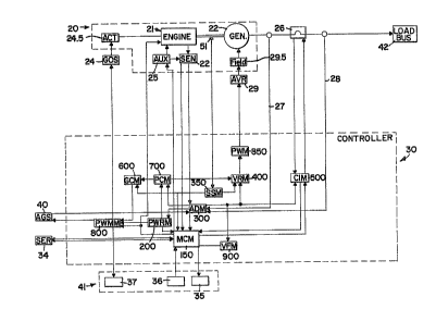
FIGURE 1 is a block diagram of an integrated gen-set
controller constructed according to the principles of the
~ ' ' ' " '
~32~
-- 10 --
present invention, wherein lines inside the hatched
controller area indicate information flow and the blocks
within that area represent modules consisting of logic
flow;
FIGURE 2 is a block diagram of the functional
characteristics of the microcontroller of the controller
represented by block 30 in FIGURE l;
FIGURE 3 is a block diagram of the functional elements
of the controller represented by block 30 in FIGURE 1
FIGURE 4 is a schematic diagram of the phase detector
represented by block 54a in FIGURE 3;
FIGURE 5 is a schematic diagram of the phase detector
and PI compensator represented by blocks 54b and 68 in
FIGURE 3 respectively;
FIGURE 6 is a schematic diagram of the automatic
voltage regulator power stage represented by block 29 in
FIGURE l;
FIGURE 7 is a schematic diagram o the governor output
power stage represented by block 24 in FIGURE l;
FIGURE 8 is a schematic diagram of the zero crossing
detectors represented by blocks 56 and 52 in FIGURE 3;
FIGURE 9 is a schematic diagram of the precision
rectifier and filters represented by block 57 in FIGURE 3;
FIGURE 10 is an electrical schematic diayram modeling
the paralleling circuit represented by block 53 in FIGURE
3;
FIGURE 11 is a logic flow diagram illustrating the
main loop of computer program operation of the gen-set
controller 30 in FIGURE l;
FIGURE 12 is a logic flow diagram illustrating the
computer program operation represented by block 204 in
FI&URE 11;
FIGURE 13 is a logic flow diagram illustrating the
computer program operation of the voltage current
regulation module represented by block 400 in FIGURE l;
FIGURE 14 is a logic flow diagram illustrating the
computer program operation of the governor control module
.
. ~ .;
' :: ,':, , :. ;
-`` 13~32~
represented by block 600 in FIGURE 1;
FIGURE 15 is a logic flow diagram illustrating the
computer program operation of the A/D service routine
represented by block 300 in FIGURE l;
FIGURE 16 is a logic flow diagram illustrating the
computer program operation of the permissive paralleling
control module represented by block 700 in FIGURE l;
FIGURE 17 is a logic flow diagram illustrating the
computer program operation of the circuit interrupter
module represented by block 500 in FI~URE l;
FIGURE 18 is graphical representation of the
appropriate time required by controller 30 of FIGURE 1 to
execute the various logical modules and further represents
an illustration of the relative time in which the modules
may be executedi and
FIGURE 19 is a graph in semi-log scale of the
relationship between the percentage of rated current being
drawn from gen-set 20 versus the time prior to circuit
interrupter module 500 opening interrupter 26.
Detailed DescriPtion of a Preferred Embodiment
Referring now to the FIGURES, there is illustrated an
embodiment of a microprocessor based integrated gen-set
controller constructed in accordance with the principles of
the present invention. The controller system is generally
referred to by the reference numeral 30. The engine and
electrical generator system, hereinafter referred to as the
"gen-set" for convenience, is illustrated in FIGURE 1 as
including an engine 21 and its corresponding electrical
3n generator 22, which in the preferred embodiment is a
three-phase brushless synchronous generator. The generator
22 may be connected in a wye or delta configuration in any
number of voltage configurations as is well known in the
art. For the purpose of this application, a 120/208 wye
3S connection will be assumed. The generator 22 is
mechanically linked to receive rotational energy from
engine 21. Engine 21 may take many forms, including using
. ~ . . : . ~., . :
. ' ~ ~. :
,~ :
~3~32-2~
gas, diesel or propane as its source of energy and may
conceivably make use of other forms of energy such as wind
power or hydroelectric. The engine and generator together
forming the gen-set 20 may be considered to have two
states. The first state is an "operational" state wherein
the engine is producing rotational energy for generator 22
to produce electrical energy. The gen-set 20 may be
connected to a load bus 42 for transmitting the produced
electrical energy. The second state is an "inhibited"
state wherein engine 21 is producing no rotational energy.
In the inhibited state, the generator 22 cannot produce
electrical energy.
The various modules and devices of a preferred
embodiment constructed according to the principles of the
present invention will be described in the following order.
First, an overview of the information flow between the
various logic modules of the controller will be described.
Second, an overview of the microprocessor chip used by
controller 30 will be presented. Third, a description of
the schematics describing the various connections to
controller ~0 will be set forth. Fourth, the various
peripheral circuits utilized in a preferred embodiment will
be described. Last, the operation and control of the gen-
set 20 by controller 30 will be described through logic
flow diagrams which may include software resident in
controller 30.
First, to describe the in~ormation flow between the
modules, and referring still to FIGURE 1, within the
hatched lines of controller 30, there is a governor control
module ~GCM) 600, having inputs from speed sensing module
~SSM) 350 and parallel control module (PCM) 700. SSM 350
receives input from a magnetic pickup 51 located on the
engine 21. The pickup 51 produces a sine wave by passing
metallic teeth close to a magnetic pickup as is well known
in the art. In a preferred embodiment, pickup 51 is
designated as model number ~YNT-13200, manufactured by
Barber Colman. SSM 350 then generates a number based on
, ;.' ~ :'
, . ,
- ~-`` 13~3~2~
the input from pickup 51 that is proportional to the
rotational speed of gen-set 20. This speed determines the
frequency. The number is then sent to GCM 600. GCM 600
calculates the throttle position for engine 21 based in
large part on the frequency received from SSM 350 (although
PCM 700 may affect this calculation as discussed below).
The throttle position output of GCM 600 is sent to the
pulse width modulator module (PWMM) 800 for subsequent
output through a high speed input-output device 43 (FIGURE
2~ resident on controller 30. The signal is sent from the
high speed input-output device 43 to the governor output
stage 24 which controls the actual throttle position of
engine 21 via ~n actuator 24.5.
Voltage regulator module (VRM) 400 receives its
fundamental input from the analog to digital converter
module (ADM) 300. ADM 300 monitors the three-phase voltage
and current produced by generator 22 via line 27 (shown as
only one line for convenience although seven lines are used
in a preferred embodiment) and provides the voltage and/or
current information required by VRM 400. VRM 400 uses the
transmitted values as the fundamental information for
determining the required output to be delivered to the
pulse width modulator (PWM) 850. The automatic voltage
regulator (AVR) power stage 29 receives the PWM 850 output.
AVR power stage 29 is connected to the field windings 29.5
of generator 22.
Also providing input to VRM 400 is SSM 350. The
information provided to VRM 400 by SSM 350 is used during
the proportional voltage drop feature of the present
invention as will be described below. Further providing
input to VRM 400 is the PCM 700. This infoxmation is
provided to VRM 400 during a paralleling operation as will
also be described below.
VRM 400 also provides for regulation of any one of the
three-phase currents as will be described below.
As discussed~ providing input to GCM 600 and VRM 400
is PCM 700. The PCM's 700 function is to assure that in
: . ! .
. ' ,~ ~ '.
13~322~
- 14 -
the event that additional gen-sets (AGS) 40 are connected
to the load bus 42, then gen-set 20 will be connected to
the load bus 4~ only if it is synchronized to the load bus
42. Furtherl PCM 700 provides for enabling load sharing
once circuit interrupter 26 is closed.
PCM 700 also provides for synchronization of the gen-
set 20 with the load bus 42. This feature is provided by a
voltage monitoring the phase difference between the voltage
waveforms on the load bus 42 and gen-set 20.
Providing control to circuit interrupter 26 is circuit
interrupter moaule (CIM) 500. Circuit interrupter 26 is an
AC contactor. This module both controls the opening and
closing of the circuit interrupter 26 as dictated by the
various other modules, but also provides for interrupting
the generator 22 from the load bus ~2 by opening the
circuit interrupter 26 in accordance with FIGURE 19. By
way of example, FIGURE 19 illustrates that there is no
interruption by circuit interrupter 26 at a current of less
than 120% of the generator's 22 rated current. Also,
FIGURE 19 illustrates that at greater than 400% of rated
current, the interrupt occurs immediately. At values
between 120~ and 400%, the CIM 500 opens interrupter 26 in
a time dependent fashion. The values indicated by the trip
curve illustrated in FIGURE 19 are stored as a look up
table by controller 30.
The voltage fault module (VFM) 900 receives input from
the ADM 300 regarding the status of the gen-set 20 voltage
being produced. This information is in turn provided to
the monitor control module (MCM) 150 which is the main
working module of controller 30. The MCM 150 receives
information from each module described thus far with the
exception of the GCM 600 and the VRM 400. It also receives
input from a module not yet dis¢ussed, that module being
the power calculation module (PWRM) 200. The PWRM 200
calculates the real and reactive power being drawn from
generator 22 and provides the information to the PC~ 700
the PWMM 800 (to drive display meters 37) and the MCM 150.
,
, . . .
.,. - , ;~,
,.
.. . .
,
-`~ lL3~3229
- 15 -
Controller 30 is also illustrated as capable of
supporting serial communications (SER) 34, fault displays
35, operator inputs 36 (typically a cathode ray tube (CRT)
device for presentation of system information to an
operator and a keyboard for operator input to the
controller), and meter drives 37. Controller 30 also can
provide starting aid to engine 21 (e.g., glow plugs or the
like). In the preferred embodiment controller 30 is an
8097 micro controller chip of the 8096 family of controller
chips manufactured by Intel.
Controller 30 is also capable of communicating with
AGS 40 and monitoring the load bus 42 to which the
generator 22 is connected. Controller 30 is illustrated as
monitoring one phase of the bus voltage and phase via line
28.
Lines 27 and 28 are connected to monitoring devices
such as ammeters and voltmeters or current and voltage
transducers which are well known in the art and which will
not be described further.
Second, is a description of the microcontroller
portion 30.1 of controller 30.
Referring now to FIGURE 2, there is illustrated a
block diagram of the 8097 microcontroller portion of
controller 30 utilized in a preferred embodiment of the
present invention. The controller is illustrated generally
at 30.1 in FIGURE 2. There are two major sections of the
microcontroller 30.1. The first i5 the CPU section
designated as 31 and the I/O section designated as 32.
Illustrated with the I/O section 32 are the functional
blocks into which the section is subdivided.
The CPU section 31 uses a sixteen bit arithmetic logic
unit which operates on a 256 byte register file. The two
are connected via a sixteen bit data bus and an eight bit
address bus. Any of the locations in the register file can
be used for sources or destinations for most of the
instructions upon which the CPU operates. This type of
architecture is known as register to register.
. . :
' -. ~ ~' ~' '
~L313~2~
- 16 -
Within the I/O section 32, there are seven major I/O
functions. The first is a high speed input (HSI) unit 43
which provides automatic recording of events. The HSI is
connected to the interrupt control 44 and the data bus.
Second is the high speed output (HSO) unit which provides
automatic triggering o~ events in real time interrupts.
Together with the HSI 43, the high speed output is referred
to as the HSIO unit. Third is the pulse width modulation
(PWM) outp~t ~5 which can be used as a digital to analog
converter. Fourth i~ the analog to digital (A/D~ converter
46 which has eight multiplexed inputs with 10 bit
resolution. Fifth is the watchdog timer 47 which operates
as an internal timer, resetting the system if the so~tware
fails to operate properly. Sixth is the serial port 48
which has several modes and its own baud generator,
providing synchronous or asynchronous links. Finally,
there are a series of standard I/O lines designated
generally at 49 to provide interface to the external world.
Many of the I/O features of controller 30 are designed to
operate with little CPU 31 intervention.
Also shown in FIGURE 2 are VSS and VCC, the
ground/reference and voltage potential source respectively
for microcontroller 30.1 VBB is provided for the A/D
converter 46 from the back-bias generator. Similarly, ~REF
and ANGND are provided for A/D converter 46. XTALl and
XTAL2 are connected to a crystal between the two inputs
providing for a clock generator for the microcontroller
30.1.
Watchdog timer 47 is provided to "reset"
microcontroller chip 30.1 in the event that the software
does not operate properly. In order to avoid resetting; a
"word" must be written to watchdog timer 47 once each 24
milliseconds running at 8 MHz. If the "word" is not
written within that period, the timer 47 will cause the CPU
31 to reset the microcontroller 30.1 operation. Tied to
the line between watchdog ti~er 47 and CPU 31 is a reset
line connected to a circuit (not shown) which detects if
~3~3~2~
17 -
the power supply (not shown) is within the allowable
voltage range. The reset line is pulled low upon applying
power to the controller 30, but goes high to reset the
microcontroller 3~.1 in the event that the power supply
provides a voltage outside of the required range.
Memory controller 50 controls the flow of information
between microcontroller 30.1 and its I/O expander chips 58,
59 ~described below), EPROM (not shown) and RAM (not
shown)~ ~he address and data are provided to these
peripheral chips in a manner which is well known in the
art, so that the process will be only briefly described
herein. Memory controller 50 uses ports P3 and P4 to
multiplex the appropriate address and data to write, or
read, to that address. The address is transmitted to a
latch (not shown) and decoder (not shown), with the decoder
using the most significant three bits to decode which of
eight peripheral chips the information is to be "read
from/written to". The latch stores the address during this
decoding. Once the appropriate chip is determined, the
address is provided and the multiplexed data is
transmitted/received. Memory controller 50 uses the EA to
determine whether internal or external memory is being
utilized, ALE to enable the address latch, BHE for
decoding, RD to read, and WR to write.
While not specifically detailed in the FIGURES, it
will be understood that the gates, chips and other
components are properly connected to appropriate bias and
reference supplies so as to operate in their intended
manner. Similarly, attendant peripheral chips re~uired for
the operation of the several mi~rochips as well as the
selection of the various resistors, capacitors and other
components will be understood to be similarly properly
connected. Finally, althou~h not illustrated, it will be
understood that the generator 22 is connected to the load
bus 42 to facilitate the generation of three-phase power.
Referring no~ to FIGURE 3, there is illustrated ~
functional block diagram of the connection between the
, .. :: . - . .
13~322~
- 18 -
microcontroller 30.1, the operator input 36, displays 35
and monitored parameters from the sensors 22 and lines 27
and 28 among others. Beginning first with the connections,
magnetic pickup 51 is connected to the HSIO unit 36 via
zero crossing detector 52. The lines from sensors 22 are
connected to Port c of an I/O expander chip 58. The inputs
from sensors 22 include the idle switch, low coolant,
service air cleaner, battery charge, AC contactor closedl
and high/low volt connection (which indicates whether
generator 22 is connected in a series or parallel winding
configuration). The I/O expander chip 58 is connected to
the microcontroller 30.1 address and data bus. By reading
or writing information to an address corresponding to the
port of the I/O expander chip, microcontroller 30.1
receives or provides information from sensors 22 and
operator input/output 41 among others. I/O expander chip
58 is used to facilitate greater input and output from
microcontroller 30.1 and its use is well known in the art
so will not be described further.
Next, there are 8 digital channels from operator
inputs 36 connected to Port a of I/O expander chip 58.
Port b of I/O expander chip 5~ is connected to
microcontroller chip 30.1 in a somewhat different fashion
than Ports a and c. Port b of I/O expander chip 58 is
connected to a 16 channel multiplexer chip 55 via ~ive
digital control lines (A through D and inhibit). This
arrangement allows microcontroller 30.1 to read sixteen
more analog channels to A/D converter section 46 via the
common channel of multiplexor chip 55.
Still referring to FIGURE 3, the eight A/D channels of
converter section 46 are illustrated as 0A through 7A.
Inputs 0A, 1A and 2A are connected to the three phases of
generator 22 via line 27 for measurement of voltage. A/D
converter 46 inputs 3A, 4A and 5A are connected to the
three phases of generator 22 for measurement of current.
Also connected to these three phases of line 24 are phase
shift detector circuits 54a. Since controller 30.1 needs
.~
`` ~3~3~2~
to monitor several other analog signals, multiplexer chip
55 is used in connection with Port b of I/O expander chip
58 to selectively monitor these other various inputs.
These additional channels comprise the phase shift detector
circuit 54a outputs, inputs from sensors 22, load bus 42
information, voltage and frequency adjustment potentiometer
67, synchronization information from the proportional-
integral compensation network 68, and load sharing
information from additional gen-sets 40.
As described, also provided to multiplexor chip 55 is
input from the synchronization proportional integral
compensation network 68 ("PI Comp"). Connected to PI Comp
68 is a phase detector circuit 54b, which is in tllrn
connected to two zero crossing detectors ~"ZCD") 56 which
receive input on lines 27 and 28 respectively. Also
illustrated are precision filter and rectifiers 57. In a
preferred embodiment, there are seven such precision
filters and rectifiers 57, one for each generator 22
voltage and current phase and one for the load voltage.
Also connected to CPU 30.1 is I/O expander chip 59.
This expander chip also has three ports (a, b, and c) of
eight lines each and provides digital outputs to the fault
displays 35, the engine auxiliaries 25 and the circuit
interrupter 26, among others.
There are four HSIO unit 36 outputs used from
microcontroller 30.1. These are utilized in the preferred
embodiment as pulse width modulators and include a pulse
width modulator for the GCM 600, a pulse width modulator
for the real load sharing data, provided to block 53, a
pulse width modulator for the reactive load sharing data,
provided to block 53, and a spare. The module controlling
the HSIO 43 is PWMM 800. The output of the resldent
hardware pulse width modulator 45 is provided to the
regulator output stage 29.
In a preferred embodiment, the I/O expander chips are
commonly designated as a 8255 chips. The multiplexor chip
is commonly designated as a 4067 type chip. An off-chip
.;
. . .
. . .
3~322~
- 20 -
~rasable Programmable read only memory (EPROM) chip (not
shown~ is used to store the logic flow program steps to
provide for the control system operation. These steps
could be stored in a read only memory location or be down
loaded to a random access memory location or tran~mitted by
another CPU. The EPROM used is a 2764 type chip
manufactured by, among others, Intel.
Third, the description of the several various
peripheral circuits will follow.
FIGURES 4 and 5 are schematics of the phase shift
detector circuits 54. These include two different
circuits, FIGURE 4 illustrates the circuit used for power
calculation and load sharing and FIGURE 5 for
s~nchronization and permissive paralleling.
The simplified power calculation circuit illustrated
in FIGURE 4 includes two comparators 70a and 70b, each of
which produce a 50% duty cycle square wave output with an
alternating current (A.C.) voltage input Vlin and V2in
known in the art. These square wave outputs are combined
by an Exclusive OR gate 71 which pro~ides for a high output
if one of its inputs are high, but a low input if more than
one of its inputs are high. With this arrangement, the
duty cycle of the output of the ~xclusive OR gate 71, will
be proportional to the phase difference of lts input
signals. The Exclusive OR gate 71 output is filtered by
resistor capacitor network 72 which provides the DC voltage
level proportional to the phase difference. Therefore, the
voltage at point 72a will be larger if the two input
signals are out of phase.
The voltage at point 72a, however, will not provide
the necessary information to determine whether the current
is leading or lagging the voltage. This information is
required for the power sharing feature, as well as
determining if a reverse power fault condition has occurred
(i.e., power is flowing into the gen-set 20 from the load
bus 42). Therefore, a D flip flop 73 is also provided to
determine whether Vlin is leading or lagging V2in. The
:. .
^ 13132~
data input to V flip flop 73 is provided by the square wave
duty cycle of comparator 70b, while the clock input is
provided by comparator 70a. Acting in the well known D
flip flop manner, D flip flop 73 either latches a 0 or a 1
S at its data input depending on whether Vlin is leading or
lagging V2in respectively. The latched data is provided to
VLL for microcontroller 30.1.
The synchronization phase circuit 54b illustrated in
FIGURE 5 has as its input two zero crossing detectors 56.
The first zero crossing detector has the monitored load bus
42 phase voltage as its input while the second has the
regulated generator 22 phase voltage as its input. The
~ero crossing detectors 56 provide 50% square wave duty
cycles. These waves are then provided to the phase
detector circuit 54b. The circuit 54b consists of an
inverter 75 and two mono-stable devices 76. First, the
output square wave from zero crossing detector 56a is
inverted in order to shift the zero point of the mono-
stable circuit 180 degrees. Normally the output of the
mono-stable device would be linear from zero volts at zero
degrees, two and one-half volts at 180 degrees, and five
volts at 360 degrees. However, since in the preferred
embodiment a -180 to +180 range is desired, a 180 degree
phase shift is provided by inverting the signal.
The inverted signal is then provided to a mono-stable
device 76a, tcommonly designated as a 54HC4538 type
device). This mono-stable 76a is connected to provide a
long pulse which is positive edge triggered by the inverted
pulse train. Providing the clear function to the mono-
stable device 76a is a second identical mono-stable device
76b. The second device 76b receives its input from a zero
crossing detector 56b for the regulated voltage oE the
generator 22. The second mono-stable device 76b is set to
provide very short durational pulses.
In operation, the first mono-stable device 76a
provides a high output signal each time the inverted signal
goes high as illustrated in FIGURE 5 at times tl and t2.
- ,,.: . .: ,. ..
' ! ' ~ ;
.. ' '.'; ~' ' ' ~ ,~
.' ,'
3 ~ 2`~ ~
- 22 -
The mono-stable 76a signal remains high until cleared by
the second mono-stable 76b signal as illustrated in FIGURE
5 at times t3 and t4. The second signal goes high when the
regulated voltage from the generator 22 goes high. In this
manner, an output square wave duty cycle is provided to
~ilter 77 from the first mono-stable device 76a. The duty
cycle is proportional to the phase difference between the
load bus 42 and the gen-set 20.
The square wave duty cycle is then filtered by a
buffer and resistor-capacitor network 77 which filters the
duty cycle to a DC voltage level. The output of the filter
at point 77a is equal to two and one-half volts when the
two waves are synchronized with each other, zero volts when
the two waves are -180 degrees out of phase, and five volts
when the waves are +180 degrees out of phase. Be-tween
these points, the voltage varies linearly.
The DC voltage level proportional to the phase
difference from point 77a is then provided to the PI
compensation network consisting of resistors 78 and 79a,
capacitor 79b and Op amp 79c. This network compares the
difference between the phase difference DC voltage level
and a fixed voltage (in the preferred embodiment, two and
one-half volts). In the event of a voltage differential,
then the network provides an error signal, including an
integral term to provide stability, to controller 30.
The signal from the PI compensation network is
transmitted as an analog voltage channel to the micro-
controller 30.1. The micro-controller samples the channel,
converts the analog signal to a digital signal, and
provides the information to the G~M to speed up or slow
down the gen-set 20 accordingly.
FIGURE 6 is a schematic of the AVR power stage 29.
Input from the pulse width modulator 45 is connected to a
positive voltage potential V~ via a diode 80 and resistor
81. Connected to the cathode of diode 80 is a zener diode
82 with its anode connected to ground Pulse width
modulator 35 is also connected to two C-Mos Schmitt trigger
'' ;'` ~ ' '
~, ,., . ~ :.
~` ~3~322~
- 23 -
gates 83, designated by part number 40106 and manufactured
by Motorola, via resistor 84. This positive line of Vpwm
is also connected to ground through diode 85. The negative
input from PWM 45 is connected to ground and also to diode
85. The trigger gates 83 are connected in parallel and are
connected to capacitor 87 and zener diode 89 which are
connected in parallel to ground. The trigger gates ~3 are
then connected through resistor 88 to the gates of two
parallel connected MOSFETS 89 with their source connected
to common Point X, and drain connected to the field
winding. Also connected to ground is an oP Amp 90
connected as an inverting amplifier sensing the voltage
across current sense resister 91 located in the current it
return path. The voltage drop across sense resistor 91 is
tied to the inverting input of OP Amp 90 and to feedback
resistors 94a and 94b. The output of OP Amp 90 is
connected via filter resistor 92 to capacitor 93 and the
field current line VFc. Capacitor 93 is also connected to
ground. Located between a point Y and the drain of MOSFET
89a is diode 95. Connected between points x and y is a
rectified quadature winding input VO'
In operation, the power stage 29 operates in the
followin~ manner. Microcontroller 31.1 uses pulse width
modulator 45 to provide a variable duty cycle to the
terminals labeled Vpwm Diode ~0, resistor 84 and diode 85
are present to suppress transients. The pulse width
modulator 45 input is applied to the Schmitt trigger gates
83 to buffer the input signal. The capacitor 87, zener
diode 89, and resistors 88 provide for filtering the signal
applied to the parallel wired MOSFETS 89. The inverted
signal is applied to the MOSFETS 89 such that at time tl of
the applied pulse width modulator 45 signal, the MOSFETS
conduct. In the preferred embodiment, MOSFETS ~9 conduct
at 10 volts. When MOSFETS 89 are conductive, a current itl
is set up through the field winding 29.5, with diode 95
back biased. VQ is a full wave rectified voltage whose
source is the quadature winding of generator 22. At time
'- ` ` '
.. .
13~ ~2~
- 24 -
t2 MOSFETS ~9 turn off. Since the winding 29.5 acts as an
inductor, the current tends to continue ~lowing, thereby
establishing current it2 ln a loop through the field
winding 29.5 and diode 95.
Turning now to FIGURE 7, there is illustrated a
preferred embodiment of the governor output stage 24 shown
in FIGURE 1. Input to the governor output stage 24 is
transmitted from HSO.O of microcontroller 31.1. This
input, designated Vpwm in FIGURE 4, is connected to an npn
transistor 103 via resistor 1020 The transistor's 103
emitter is connected to ground and its collector is
connected to a series connected zener diode pair 104. The
collector is connected to the series diode pair which is
connected in parallel with resistor 105 and pulse
transformer 106.
A positive voltage potential source V+ is connected
via resistor 108 to zener diode 104b anode. The secondary
winding of transformer 106 is connected to the source an~
gate of power MOSFET 107. Power MOSFET's 107 drain is
connected to the parallel connected group of capacitor 110,
resistor lll, and cathode to cathode series zener diodes
112 (specifically diode's 112a anode). Power ~OSFET 107 is
also connected to the gate of power MOSFET 113. MOSFET 113
has its source connected to the gate of MOSFET 107. The
voltage source V+ is connected with its anode to MOSFET's
113 source~ and cathode to the cathode of diode 114 and to
the winding of actuator 24.5 for engine 21.
In operation, microcontroller 30.1 provides a variable
duty cycle by using HSIO unit 43 as a pulse width modulator
drive. The resulting duty cycle is applied at Vpwm. The
pulse width is applied via biasing resistor 10? to
transistor 103 which acts in the classic transistor manner,
wherein the transistor is saturated when the input level is
high thereby producing a low voltage at its collector, and
being cut o~ when the voltage input is low thereby
producing a high voltage at its collector. The voltage
source V+ current is limited by resistor 10~ when
' ~ '
: ~ - - . .
13~322~
- 25 -
transistor 103 turns on. Resistor 105 dissipates energy
stored in the pulse transformer 106. The zener diode pair
104 acts to clamp the voltage after transistor 103 turns
off and the pulse transformer 106 flys back.
The output of pulse transformer 106 is indicated at
point Vl as a series of pulses decaying exponentially for
each change in input voltage Vpwm. The positive pulse at
time tl is generated by transformer 106 is provided to
charge capacitor 110 through the intrinsic diode of MOSFET
107 thereby turning on MOSFET 113.
The pulse Vl decays to zero, but MOSFET 113 stays on
due to capacitor 110 being charged. At time t2 transistor
103 turns off allowing pulse transformer 10~ to fly back
through the combination of resistor 105 and diodes 104. A
negative pulse is generated which turns on MOSFET 107,
thereby discharging capacitor 110 and turning off MOSFET
113.
The output of MOSF~T 107 at its drain is indicated at
point V2. The zener diode pair 112 are present to suppress
transients. The resulting duty c~cle o~ point V2 is
applied to the gate of MOSFET 113 turning MOSFET 113 on and
off as described above Therefore, at time tl current it1
is established around the loop formed by voltage source
116, actuator 24.5 and MOSFET 113. When MOSFET 113 cuts
off, actuator 24.5 acts as an inductor and the current
continues to flow around the loop through diode 114 as
indicated by it2.
Referring now to FIGURE 8, there is illustrated a
preferred embodiment zero crossing detector 52 and 56. The
voltage waveform applied to the circuit, Vin, is connected
to resistor 118 which is in turn connected to the parallel
connected capacitor 119 and diode 120 to ground and to
resistor 121. Resistor 121 is connected to the parallel
connected diode 122 and resistor 123 to a voltage source
V+. The voltage source is connected to the non-inverting
input of comparator 129 via resistor 124. Also connected
to the non-inverting input of comparator 124 is resistor
'.
.
' ': '' , ', :, .
-" ~3~322~
- 26 -
128 to a ground/reference potential and hysteresis resistor
127. Hysteresis resistor 127 is connected to the output of
comparator 129, VOut and V+, to the latter through resistor
125. Resistors 118, 121, 123, 124 and 128 are provided to
allow for use of the circuit as a zero crossing detector
with a single supply voltage
In operation, Vi is compared to a voltage by
comparator 129 such that when the input voltage is greater
than zero volts, the output VOUt is zero or low. When the
input voltage is less than zero, VOUt is high. The output
voltage changes from low to high or high to low each time
the input waveform voltage crosses through zero volts.
VOUt is kept from oscillating by adding hysteresis resistor
127.
Referring now to FIGURE 9, there is illustrated a
preferred embodiment precision rectifier and filter 57.
The voltage Vin is connected to resistor 130 which in turn
connected to zener diode 131 to ground, resistor 132 to Op
amp 134 and feedback resistor 133. The output of OP amp
134 is supplied to the anode of diode 135 which ls
connected to ground via resistor 136, feedback resistor 133
and resistor 137. The latter is then connected to
capacitor 138 to ground and to a unity gain buffer to VOUt.
In operation, the Op amp 134 is connected as an
inverting amplifier which is inoperative when Vin is
positive, the resulting waveform at Vl is proportioned to
input waveform Vin with resistors 130, 133 and 137 acting
as a voltage divider. When Vin is negative, Op amp 134
acts as an inverting amplifier. The result at Vl is a full
wave rectified voltage. In operation, diode 135 isolates
the Op amp 134 during the positive portion of the Vin
waveform. Resistor 130 and zener diode 131 provide
transient protection. ~he rectifiéd wave is then filtered
by the Resistor 137 and capacitor 138 combination.
Finally, the filtered wave is buffered by the unity gain
buffer 139.
Next referring to FIGURE 10, A~S 40 are connected in
~3~322~
- 27 -
parallel to the load bus 42, the controller 30
automatically compensates so that each gen-set 20 and
additional ~en-set 40 shares real power and reactive power.
- The governor output stage 24 of controller 30 is adjusted
to share the real power and automatic voltage regulator 29
is adjusted to share the reactive power. The total power
supplied by each gen-set 20, 40, will equal the power
multiplied by cosin~ ~ plus the power multiplied by sine ~;
where cosine ~ is the real power and sine ~ is the reactive
power~ Therefore, to calculate real power, the magnitude
of phase A voltage multiplied by the magnitude of phase A
current is multiplied by the cosine of the angle between
that voltage and current. Similarly, the reactive power is
found by taking the phase A voltage times the phase A
current multiplied by the sine of the phase difference
between the voltage and current. This is provided in a
similar fashion for the other two phases. PWRM 200
provides this information to the PWMM ~00 for output in a
pulse width form for real power meter 37 and to PCM 700
which in turn provides the power information to the VRM 400
and GCM 600 to share power, and to MCM 150 for reverse
power fault analysis.
The simplified model of the parallel circuit used in
the preferred embodiment is best seen in FIGURE 10. The
gen-set 20 includes a current source 230 which generates a
current which is proportional to the real power for voltage
gen-set 20. The input for current source 230 is determined
by a square ware duty cycle generated by HSIO 43, which in
turn is transmitted information from the PWRM 200. In the
preferred embodiment, the pulse width modulated input VkW]
is proportional to the power. Vkwl is filtered to provide
a DC voltage level. There is a resistor 231 which is
connected directly across the current source. Similarly,
there is a corresponding current source 240 and resistor
241 for the AGS 40. The voltage Vpl and Vp2 across
resistors 231 and 241, respectively, are provided to
differential Op amps 232 and 242 respectively. Vkwl is
.
;
!,
~ 3~322~
- 28 -
also provided to Op amp 232 and Vkw2 is provided to Op amp
242. Also provided are relays 233 which are operated by
PCM 700, as described below. Generally the relays 233 are
closed only after gen-set 20 is in parallel mode, and the
gen-set is synchronized with the load bus 42 ti.e.~ after
load sharing has been enabled).
In operation, when the voltages Vkw2 are the same,
current sources 230 and 240 will be producing identical
currents. In that instance, the voltages Vpl and Vp2
across the resistors will be identical and there will be no
current flow Ip through the parallel cables between gen-set
20 and AGS 40. However, if the load on either gen-set 20,
40 is greater than the load on the other, then a current Ip
will be established to provide an equal voltage Vp across
the resistor with a smaller current flowing through it from
its companion current source. Since Vpn will be larger
than Vkwn on one set, and smaller on the other, the
respective differential Op amps 232, 242 will provide
appropriate voltages VILsN to their respective controllers
for processing. As can be readily appreciated by those
skilled in the art, in the modeled circuit VILs will equal
Vp less Vkw. In order to share both real and reactive
power, duplicate circuits are required.
~y way of example, if the real load on additional
gen-set 40 increased, the voltage Vkw2 would increase and
so would the current generated by current source 240.
Since resistors 231 and 241 are in parallel, the voltages
across them must be equal. Therefore, current Ip would
flow as indicated in FIGURE 10 to balance the system.
Since Vpl would be larger than Vkwl, VILsl would be
positive. Conversely in the given example, VILs2 would be
negative.
This VILsl signal is provided to the ADM 300 which
provides the information to the PCM 700. GCM 600 balances
the real power by utilizing the information by modifying
its reference frequency as described below. At the same
time, AGS 40 senses that the voltage across resistor 241 is
13~L322~
- 29 ~
smaller than Vkw2 Therefore, this inEormation may be sent
to its controller in turn to provide an opposite
correction.
In this manner, any number of AGS 40 may be connected
to the generator controller 30, in parallel, such that the
real and reactive loads will be shared. Further, the
parallel function will also operate with existing analog
systems using such a parallel model.
Referring again to FIGURE 1, as discussed above,
within controller 30 is illustrated the information flow
between the various modules. The modules represent various
operational characteristics of controller 30. In a
preferred embodiment constructed according to the
principles of the present invention, these modules may be
executed utilizing software instructional logic. The logic
flow diagram of an embodiment of the program logic which
might be resident in system controller 30 is illustrated in
FIGURES 11 through 17. FIGURE 11 illustrates a logic flow
diagram of the steps taken by controller 30 to cause the
gen-set to undergo a change from an inhibit state to an
operational state. Next will be a description of the
operation process of the gen~set 20 in connection with the
several logic flow FIGURES.
After first started at block 201, controller 30 then
proceeds to initialize its variable registers and memory at
block 202. The controller 30 must initially Eorce the
interrupts of the analog to digital converters and the high
speed outputs. Also, the SER 34 and HSI 43 must be
enabled.
At block 203, after the initialization period, the
preferred embodiment performs a serial time-out check.
Since the SER 34 is interrupt driven, CPU 31 must check to
determine whether the SER 34 buffer should be cleared to
enable the buffer to receive a message.
At block 204, controller 30 branches to the engine
control monitor routine 150. Upon return from the engine
monitor control routine 150, at block 205, controller 30
~32`~
- 30 -
goes back to serial time-out check block 203 to repeat the
process. In this manner, the processor 30 continues until
interrupted by one of the asynchronous interrupts or the
operator either resets or removes power from the controller
30. Even in the inhibited state, the controller 30
continues through this process. The asynchronous
interrupts occur upon receipt of information by the SER
port 34, the pulse width modulator routine for HSIO unit
36, and the HSIO unit 36 for frequency of the rotation of
the motor.
Referring now to FIGURES 1 and l9, the asynchronous
interrupts will be described in order to further illustrate
the operation of gen-set 20. The first asynchronous
interrupt is provided by the SER 34 and SER module 48. In
the event that a message is received via SER lines 34, then
an interrupt signal is generated by interrupt control 44 to
handle the incoming communication. An interrupt handling
routine (not shown) is jumped to for handling of the serial
information. The information is handled and controller 30
returns to its place prior to the interrupt. As
illustrated in FIGURE 18, the time required to run the
routine is typically less than 80 microseconds. During
initialization, block 201, the communications port 48 is
set up by writing a byte to a register indicating the mode
in which the port is to be operated.
The second asynchronous interrupt is the pulse width
modulation routine for the HSIO 43. This interrupt occurs
initially upon being "forced" at initialization block 201.
At that time, the HSIO 43 is "told" to interrupt after 3
milliseconds and to turn on at that time (i.e., provide a
high output voltage state). The module calculates the duty
cycle to be transmitted to the engine governor 24, meters
37 and the paralleling signal for both real and reactive
power. As illustrated in FIGURE 18l the time required to
run the routine is typically less than B0 microseconds.
The module after calculating the duty cycle writes to the
HSIO 43 to turn off after a period of time, but to turn on
--- 3L3~3~2~
- 31 -
and interrupt again aEter 3 more milliseconds. In this
manner the module sequentially interrupts the main program
every 3 milliseconds.
The third asynchronous interrupt is the HSIO 43 from
the magnetic pickup 51. The output of magnetic pickup 51
is a series of voltage pulses. In the preferred
embodiment, there are 100 teeth on pickup 51 and the gen-
set rotates at 1800 revolutions per minute (30 revolutions
per second) in its normal operative state. The HSI 36
generates an interrupt after every eight pulses or
approximately 375 times each second. This corresponds to
an interrupt occurring approximately once each 2O67
milliseconds. As illustrated in FIGURE 18, the time
required to run the routine is typicall~ less than 80
microseconds. The interrupt handling routine (not shown)
calculates the period between the last time that the
routine was implemented and when the routine was currentl~
called. Once the time period is known the frequency may be
easily ~alculated.
~0 The analog digital service routine is illustrated in FIGURE 15 starting at block 300. At block 301, A/D
service routine enables the high speed output 43 interrupt.
This is done eor two reasons. First, enabling the HSO 43
interrupt provides for a larger pulse width range to the
high speed outputs 43, and second, normally in an interrupt
routine further interrupts are not allowed so this
interrupt must be specifically enabled. Next at block 302,
A/D service routine 300 calculates when the next A/D
interrupt should occur. At block 303, the next A/D channel
in the cue of twenty-three analog channels is read. At
block 304, a logical A~D is performed between the ~/D index
and the binary number three to determine whether it equals
either zero or two. In the event that it equals zero, the
VRM ~00 is executed at block 3Q5. However, if the logical
operation equals two, the GCM 600 is execute~ at block 306.
In the event that the logical operation results in neither
zero or two, then block 307 is executed to increment the
. , , . ;. :,
~3~3~
- 32 -
A/D pointer to the correct sample table (i.e., one of four
available sampling tables illustrated in Table 1). At
block 3081 the largest currents of the three phases being
drawn from generator 22 is determined by looking at the
S latest current stored. At block 309, the largest current
is compared to 300% of the rated current for the gen-set
20. In the event that it is larger than 300%, the A/D
service table is changed in order to regulate the largest
current being drawn from generator 22. The A/D service
table is illustrated as Table 1 below.
~: ,;
:
~3~3~
- 32a ~
CJ .r~
~ ~ ~ ~ P ~ ,
H ~
~ ~ ~ Ql
t~l N~`1N
(g o a) aJ a~ ~ a
~1 ~1 H :~ O ~ Ql Q- 14 ~ C2
~`J N~ ~
O oO O
N ~~`1~ I I I I I I I I ::
cn
~1 ~1~1_I u~ o
C~
~r u~
00 ~0oOC~ .
i
r~ I~I~
Q~
ul a~
D tD ~ Ul
r-l ~1_I r-l rt N
U~
In ~ V
~1~1 ~ ~ ~ r~ O
~1 ~ ~ r GJ a) u~ g W
~1 ~~1 ~1
W ~ ~ ~ ~ ~ ~ ~.. ' ~ o
N ~
r-l~1 ~ ~, 5 h ).~ O
~1 ~1~1~1
~t
I I I
O O O O
aa a~ O ~ N
~1 ~ -1 ~J
W ~ ~ G~ a~
æ co co OD co
O r~
W ~ ~ ~ In
~ O
æ
C9, ~r
~n O
l ~ ~ ~ ~ ~ ~ ~
I
¦ N N. NN U~ 0 U~ U3 U~
,~,1 ~ s ~:: ~ h ,~
~ ~ ~ P~ ~ P. ~,
O ~ ~ ~ Ln ~ c:
~ ~ ~ a) ~ ~ ~ ,~
E~ ~ Oi) 0
z
O ~) V ~ ~ h ~
~ ~ ~It~1~ r~l ~ 1~1 h h h V 1~3
o ~ I a.) oa,l lD g g ~ -' ~
U ~ ~ ~ ~ O
i-l O I ~ ~U .~.~1 .
~ ~ ~ ~ I I I I I I ~ I
''' : ' '' ,
:, '
~3132~
- 33 -
In the event that the largest current is less than or
equal to 300%, then A/D servlce routine 300 compares the
A/D index to a constant to determine if the PWRM 200, the
paralleling module 700, or the CIM 500 should be executed.
S This is done by comparing the A/D index to different
constants at blocks 311, 313, and 315. In the event that
the A/D index is equal to that constant in the associated
module, then that module will be executed at blocks 312,
314, or 316. In this manner, one of the three modules will
be executed once eacn time through the 23 A/D channels are
read. At block 317, the ne~t off chip analog channel is
addressed. Finally, at block 31~ the A/D index is
incremented and the program returns from the interrupt,
generated by the A/D service routine 300, to the point in
the logic flow program from which it was interrupted.
MCM 150 is the next basic control program which is
executed each pass through the main control loop
illustrated in FIGURE 11. It controls reading operator
input, controlling the circuit interrupter 26 to connect
the gen-set 20 to the load bus 42, and it calls the CIM 20,
the PWRM 200, the PCM 500, and the check speed sensing
module (not shown).
As best seen in FIGURE 12, there is a logical flow
diagram of an embodiment of the program which might be
resident in controller 30. Logic flow diagram 150
illustrates the steps taken to perform the basic control
program for the gen-set 20. The program begins at 151
after being called by block 203 branch to monitor control
illustrated in FIGURE 11. At the start of each pass
through the module 150, the watch dog timer 47 resident on
the microcontroller 30.1 is reset at block 151. At block
152 controller 30 checks for override status for faults and
faults to the generator 22 or engine 21. At block 153, MCM
150 looks for operator inputs 3~ such as a lamp test/fault
reset. In the event a response is called for, then
controller 30 sends the appropriate signals. Next at block
154, processor 30 checks for faults and an "O.K. to close"
~3~322~
- 34 -
variable from the PCM 700. If both allow, and the operator
has closed a circuit interrupter switch ~not shown), the
circuit interrupter 26 is closed.
At block 155 of logic flow diagram 150, processor 30
checks the status of the circuit interrupter flag. If the
flag has been set, processor 30 executes the CIM 500 at
block 156. The CIM is described below.
If the flag has not been set~ processor 30 continues
to check the status of the power calculation flag at block
157. If the power calculation flag has been set, the P~RM
200 is executed at block 158. The PWRM (logic flow not
shown) is executed by use of a lookup table to store the
value of the sine~; where ~ equals angles 0 through 180
degrees. Since the cosine is 90 degrees out of phase, this
table may also be used for that calculation, as is well
known in the art.
If this module's flag has not been set, processor 30
moves onto check the paralleling flag at block 159. The
PCM 700 is described below. If the paralleling flag has
been set, the PCM 700 is executed by processor 30 at bloc~
160, and continues to block 161 if the paralleling flag has
not been set.
At block 161, the speed flag is checked by processor
30 and continues to execute the check speed module (not
shown) if the flag has been set at block 162. The check
speed module reviews the last several values and determines
if the gen-set 20 speed is excessive. Processor 30 then
returns to the main program loop at block 204 from block
164 after latching faults from the various modules at block
163.
It should be noted that the analog to digital
servicing routine 300 interrupts synchronously every one-
half millisecond in the preferred embodiment. Further, the
circuit interrupter flag, power calculation flag,
paralleling flag and speed flag are also synchronous such
that those modules are run after a set number of iterations
through the ADM 300. In a preferred embodiment, each of
: ' '. ' . ~,, .
. ~ . . .. .
~3~32~
- 35 -
the modules are run every 16 milliseconds. Therefore, as
illustrated in FIGURE 12, when processor 30 executes one of
modules at blocks 156, 158, 160, or 162, it would indicate
that a certain number of cycles had been performed.
Illustrated in FIGURE 13 is the logic flow diagram for
an embodiment of GCM 600. The logic flow diagram
illustrates the steps taken to calculate the value sent to
the PWMM 800 from the signals received from SSM 350 and PCM
700.
The computer program is shown generally at 600. It is
started at block 401 after being called by block 306 of the
A/D service routine module 300. First, at block 602, the
interruptions are disabled. At block 603, an error
frequency; Vl, is calculated by subtracting the actual
frequency transmitted by SSM 350 from a set reference
(GREF). As descrlbed above, the GCM 600 uses a three-mode
controller, more commonly known as a PID controller for its
proportional, integration and derivative terms. Solving
for the PID control equation~ at bloclc 604 controller 30
determines intermediate results required by the PID
algorithm utilized by controller 30 and the output Ul.
Next at block 605 o~ logic flow diagram 600, the output
calculated at block 604 is compared with maximum and
minimum outputs and corrected (clamped) to be within those
outputs if it exceeds the same. The output is then sent to
PWMM 800 to be transmitted via HSIO 43 to the governor
output stage 2~. This stage 24 operates as described above
and is based on the duty cycle that controls the actuator
24.5 to determine the speed of engine 21.
Continuing to block 606, further intermediate results
are calculated. These results are calculated subsequent to
clamping Ul and transmitting the value to provide for an
output calculation which is more recent in real time to the
engine's 21 condition. At block 607, a comparison is made
of the base reference frequency to any adjustments made by
the operator and is stored as an intermediate value.
At block 60~, controller 30 determines i~ a "soft
:
:: .
... .
,
.' ' ' ' .
: .
~3~32~
- 36 -
start routine'l is required. If the engine 21 has been in
the inhibited state and is now beginning to transmit
rotational energy to generator 22 but has not reached the
desired frequency of the system, then soft start routine
allows for engine 21 to increase its frequency in a more
gradual manner without over shooting. To do so, the soft
start reference frequency is adjusted in increments each
time through the logic flow diagram 600 at block 609 until
after a certain number of cycles, the soft start reference
is equal to the desired governor reference. At block 610,
added to the intermediate governor reference is the
parallel offset number generated by parallel PCM 700 for
synchroniæing the gen-set 20 to the load bus 42 and for
sharing real power with additional gen-sets 40. At block
611, GCM 600 ends and returns to the A/D service routine
module 300 at block 307 of FIGURE 15.
Turning now to FIGURE 14, there is illustrated a logic
flow diagram of an embodiment of the program module for
voltage regulation which might be resident in controller
30. The logic flow diagram 400 illustrates the steps taken
to perform the control PID equation for voltage and current
regulation. The program 400 is similar to the GCM 600 logic
flow diagram, however/ instead of using frequency as an
input, voltage regulation logic flow diagram 400 uses out
phase voltage of generator 22 as an input. As illustrated
in FIGURE 14 at 401, all interrupts are first disabled
except the HSO 43 which has already been enabled at block
301 of FI~URE 15 ~to provi~e for a larger pulse width
range). Next at 402, the logic flow diagram 500 first
makes a determination of whether to regulate voltage or
largest current by comparing the current to a preset
current llmiting reference number In the preferred
embodiment~ the current limiting number is 300% of the
generator's 22 rated current. This reference number is
used to determine if the current regulation mode is
required.
If the current is larger than the reference current
~ 3~322~
- 37 -
limit, controller 30 proceeds to block 403 setting the
current limit refe-ence number to 150~ of the generator's
22 rated current and changing the voltage regulation for
soft start. When the current becomes less than or equal to
the new current limit reference number, then controller 30
will return to voltage regulation at block 402 as described
below. By using a different value for the current limit
reference number, "hysteresis" is a~ded to the program in
order to avoid controller 30 oscillating rapidly between
voltage and current regulation in successive iterations
through VRM 400. Next at block 404, microprocessor 30
determines if it is the first pass through the current
regulation mode. If it is the first time (i.e., irst
iteration in the current regulation mode), then the
coefficients for the controlling PID equation are changed
at block 405, to increase the s~stem performance during the
current regulation mode. After changing the coefricients,
controller 30 proceeds to block 406. If the system has
already entered current regulation mode, block 405 is
bypassed from block 404 and proceeds directly to block 406.
Processor 30, at block 406, then calculates the error
signal by subtracting from a reference current the actual
magnitude of the regulated current. The result is an
intermediate value, Vl, which is used in the PID equation.
At this point, the current regulation rejoins the main
voltage regulation path at block 40g.
At block 402, if the current is not larger than the
compared reference limit, controller 30 sets current
regulation at 300% at block 407 and changes the PID
coefficients for voltage regulation. Next at block 408 of
logic flow diagram 400, the controller 30 determines the
error voltage by subtracting from a reference voltage the
actual regulated voltage. The result is Vl which is used
in the PID equations at block 409.
At block 409, intermediate values of the PID equation
necessary for the algorithm are calculated and the output
Vl for the PWMM 850 is determined. Next at block 410, the
,. . - :
,. ..
13~3~2~
38 -
output i9 compared to the maximum and minimum pulse widths
allowed by pulse width modulator 45 and is limited
accordingly ~clamped) to be within those maximum and
minimum ranges. At block 411, further intermediate values
are calculated. At block 412, an intermediate voltage
reference is set equal to the stored base voltage plus any
operator input voltage level. The VRM 400 has provisions
for accepting a digital reading of a voltage adjust pot
setting (not shown). It uses this input to adjust th~
intermediate voltage reference, thereby allowing an
operator to adjust the reference voltage without having to
enter the software. At block 413, soft start reference
voltage is compared to the intermediate voltage reference
calculated at block 412. If the soft start reference
voltage is less than the voltage reference the soft start
reference voltage is incremented at block 414 and
controller 30 moves to block 415. However, if the soft
start refere~ce voltage is larger than the voltage
reference, then the soft start is complete and the soft
start reference is not incremented but rather controller
moves directly to block 415. The soft start function
operates when the gen-set is first started from the inhibit
state to the operational state as described above. The
reference voltage is started at zero and is then
incremented slowly to the base reference voltage (in the
preferred embodiment 120 volts). The device operates in
this manner in order to provide that the voltage does not
overshoot the voltage reference on start-up.
At block 415 processor 30 determines whether there has
been a drop in engine speed (frequency). In the event of a
frequency drop (e.g., due to a heavy load drawing real
power from gen-set 20), processor 30 will also drop the
voltage in order to allow the engine 20 speed to regain the
appropriate reference speed. In other systems, when a
heavy load is placed on the engine, and the engine speed
drops, the voltage does not decrease. In some cases
causing the engine to lug or stall. However, by dropping
-' 13~322~
- 39 -
the voltage with the engine 20 speed, the load is reduced
and the engine 20 is allowed to recover to the appropriate
reference frequency. This relationship of reduced voltage
to engine frequency is a linear function (e.g., the voltage
drops linearly with the frequency). In the preferred
embodiment, the voltage is independent of the frequency
above 59 Hz. Below 59 Hz, the vol-tage is decreased
linearly by approximately 2 volts per Hz.
At block 416, determination is made whether there has
been a drop in frequency and if so whether it is smaller
than the soft start reference. The voltage reference is
then set equal to the lower of the frequency reference and
soft start reference numbers at block 417 and 418
respectively. Processor 30 then continues to block 419
where the next reference voltage is set equal to the lesser
of the frequency reference or the soft start reference.
Additionally, the parallel offset values received from the
PCM 700 are added for reactive land sharing. At block
41~, processor 30 then returns to the A/D service routine
300 at block ~05 of FIGURE 15.
Paralleling control module 700 executed at block 160
of logic flow diagram 150 as illustrated in FIGURE 12 is
set ~orth in a logic flow diagram of an embodiment of the
routine logic which might be resident in controller 30.
Logic flow diagram 700 illustrates the steps taken to
perform a permissive paralleling process between multiple
gen-sets. The program starts at block 701 and proceeds to
block 702 where it determines if processor 30 is in a
single or parallel mode. In a preferred embodiment, this
is determined by a physical two pole switch. If the gen-
set 20 is in the parallel mode, processor 30 continues to
block 703 where it determines whether the load bus 42 is
energized. If the load bus is not energized, the
controller 30 sets the OK to close contactor flag at block
708 and returns to the MCM 150 at block 161 of FIG~RE 12.
If the load bus is energized, processor 30 then determines
if the contactor is open at block 704. If the contactor i5
", , . ' , .
, . ':' ~ ,.. ...
:.: - , , ... i ~.
~ ~3~L32~
- 40 -
open and the load bus 42 is energized, then the
synchronizer must be operated prior to closing the
contactor~ Therefore, at block 705, the synchronizer is
operated by determining the value of x = 2.5 - VOUt where
VOUt is provided by the circuit illustrated in FIGURE 5.
The resulting value x is supplied to block 610 of FIGURE 13
to appropriately speed up or slow down gen-set 20.
If the contactor is closed, controller 30 determines
if there is permissive paralleling at block 706. If yes,
at block 707, processor 30 then determines whether the
gen-set 20 has achieved the permissive parallel standards
for a set time period, in the preferred embodimen-t one-half
second. A time delay is required to insure that the gen-
set 20 is actually synchronized with the load bus 42 and
that they have not merely appeared to be synchronized for
an instantaneous period. If it is within range for the set
period of time, then a further determination on the status
of the contactor is made at block 709. If the contactor is
already closed, then at block 710 the load sharing is
enabled by subtracting the VILs from 2.5 volts (the zero
point if the sets are balanced) and the paralleling relay
233 are closed If the contactor is not closed, set the
"O.K. to close" contactor flag and open paralleling 233 at
block 711. In either event, the program then returns to
the MCM 150.
In the event that the permissive paralleling standards
are not met at block 708, processor 30 returns to monitor
control program at block 719. If there is no permissive
paralleling at block 706, th~n at block 712 the controller
30 sets the not OK to close contactor flag and resets the
time delay. Controller 30 then returns to the MCM 150.
At block 702, if the physical switch (not shown) is in
the single mode position controller 30 resets the time
delay at block 713 in order that if the switch is moved to
the parallel position, then the controller 30 is ready to
determine whether the permissive paralleling conditions
have been satisfied. Controller 30 then continues to block
..,,,,.~.' ', . ~
:, ~
:
- ~3~
- 41 -
714 where processor 30 determines whether the bus is
energized. If the bus is not energiæed, then the "OK to
close" contactor flag is set at block 715 and processor 30
returns to the monitor control program at 717. If there is
a voltage potential on the bus and the processor 30, at
block 716, sets the not OK to close contactor flag and
returns to the monitor control program 150 at block 717.
CIM 500 is called at block 156 of MCM 150 in FIGURE
12. ~ logic block diagram set forth in FIGURE 17 which
encompasses logic which may be resident în controller 30
for CIM 500.
Controller 30 begins the CIM 500 at block 501 and
moves to block 502 to determine whether the largest current
being drawn from generator 22 exceeds 400 percent of the
rated current for gen-set 20. In the event, that the
lar~est current is greater than 400 percent, then
controller 30 moves to block 503 to open the interrupter
and to indicate a fault to operator displays 35.
Controller 30 then returns to MCM 150 at block 505.
However, if the current is not larger than 400 percent of
the rated current for gen-set 20, then at block 50~, a CIM
variable is set to an initial look-up table value and a
second variable, called trip timer count, is initializedO
Next, at block 506, controller 30 determines if the load
current is larger than the percent rated value from the
look-up table for the corresponding trip count. If it is
not, the controller 30 goes to block 507 to determine if
the trip timer count is greater than zero. If it is not,
controller 30 proceeds to block 512. If the trip time
count is greater than zero, however, controller 30 goes to
block 508 to decrement the trip count timer. Back at block
506, if the current is larger than the percent rated from
the look-up table, then controller 30 proceeds to block 509
and increments the trip count timer. Next, at block 510,
if the count in the look-up table is greater than the trip
number stored in the look-up table, then the CIM flag is
set at block 511. However, at block 510 where the count is
,; ~ , :- , , ~ . ; ,
~3~ 3~
- 42 -
compared to the trip number, if the count is not larger
than the trip number, then controller 30 continues to block
512. Finally, at block 512, controller 30 determines if
all table values have been checked. If not, then
controller 30 returns to block 506 and repeats the process
of going through blocks 506 through 512 until each o~ the
look-up table values have been checked.
In this manner, the CIM 500 iteratively looks at each
table value in order to determine if the current has been
higher than the rated time-current relationship for gen-set
20 as illustrated in FIGURE 19. It does so by incrementing
the trip count timer for each iterative pass through the
CIM 500 loop where the current i5 greater than the percent
value rated from the look-up table. If the trip timer is
incremented a set number of times, such that it e~ceeds the
look-up trip number for that pass through the loop, then
the CIM flag will be set at block 511.
On the other hand, when the current is not larger than
the percent rated from the look-up table at block 506, then
the trip count timer is decremented for those values, so
long as it is greater than zero, and the CIM flag will not
be set, unless it has previously been set.
Proceeding from block 512 after each table value has
been checked, controller 30 determines if the CIM flag has
been set at block 513. If it has not been set, then
controller 30 returns to the MCM at block 514. However, if
the flag has been set, then controller 3Q determines if an
overload or short circuit has occurred and sets the
overload or short circuit return flag accordingly. At
block 516, the contactor 26 is opened. Finally, at block
517, controller 30 returns to MCM 150.
Although the controller 30 has been characterized by
such terms as preceding, returning and moving, those
skilled in the art will appreciate that these terms are
used to describe the operation of controller 30 while
processing the various programming steps illustrated by the
various logic flow diagrams.
:
~ .
43 -
It is to be understood that even though numerous
characteristics and advantages of the present invention
have been set forth in the foregoing description, together
. with details of the structure and function of the
invention, the disclosure is illustrative only and changes
ma~ be made in detail, especially in matters of the
regulation of different phases of the generator 22, the use
of synchronous or a synchronous interrupts for the various
modules, the method and order of sampling the various
system parameters, the use of positive or negative logic,
and the supporting hardware and software routines and data
structures, to the full extent indicated by the broad
general meaning of the terms in which the appended claims
are expressed.
:- .
,, ,' ', ' :
: . ::
, . . .. .
., ..:
:, ,. i, ,