Note: Descriptions are shown in the official language in which they were submitted.
- 1 - RCA 84727/84727A
INTE:~POI~TOR FOR CO~IPRE8S D VIDEO DATA
The present invention relates to interpolators
for expanding video data.
D.L. Sprague, N.J. Fedele and L.D. Ryan in a U.S.
Patent 4,790,832 issued April 26, 1988, entitled "IMAGE
STORAGE USING SEPARATELY SCANNED LUMINANCE AND CHROMINANCE
VARIABLES" describe a system for retrieving stored images
in digital form from video random access memory (VRAM). A
VRAM is a dual-ported memory including a dynamic
random-access memory with a random-access read/write port.
It also includes a relatively small, auxiliary, static
serial memory with a serial output port. The auxiliary
memory can have its storage locations loaded in parallel
from any row of storage locations in the larger dynamic
memory upon command. Thereafter the auxiliary memory has
its storage locations scanned by a counter operating as an
address generator and is read out in a shift register
operation to supply a stream of video data.
In the Sprague-Fed~le-Ryan system, images are
described in terms of luminance and chrominance components,
each of which has its own bit-map organization associated
therewith in the dynamic memory portion of VRAM. Groups of
bits descriptive of the luminance or chrominance of a pixel
are stored together in a conformal mapping of the display
in a "bit-map-organized" memory as that term is employed in
this specification. The luminance components are generally
more densely sampled in image field space than the
chrominance components are. This is done to conserve image
memory, recognizing that visual acuity for chrominance is
less than that for luminance.
VRAM is "linearly packed"--i.e., the raster
scanning of pixel codes is stored in successive rows of the
dynamic memory. Rows in dynamic memory do not necessarily
have a 1:1 correspondence with scan lines in the ultimate
display. A formatter known as a "pixel unwrapper" takes a
-2- RCA ~g727/~727A
stream of data supplied to lt from ~he VRAM serial oukput
por~ and passes it into scan lines of successive pixel
codes.
During line trace intervals in the display, VRAM
supplies data from its output port from which data the
pixel-unwrapper generates a stream of pixel codes
describing luminance in real time. During selected line
retrace intervals in the display, VRAM supplies data from
its serial output port from which data the pixel unwrapper
generates two streams of pixel codes describing chrominance
in a compressed-in-time and advanced-in-time format.
Each stream of chrominance components is supplied
to a respective chrominance re-sampling apparatus. Each
re-sampling apparatus comprises a respective odd-line
line-storage memory, a respective even-line line-storage
memory and an interpolator.
Successive lines of each stream of compressed
chrominance data are selected on an alternating basis for
writing into its odd-line or its even-line line-storage
memory. These line storage memories act as a rate-buffer
to supply samples to their interpolator. The interpolator
generates samples of the chrominance component with
compression removed and with delay to temporally align them
with the real-time luminance samples.
The luminance samples and the two sets of
chrominance samples are converted from digital to analog
form and are linearly combined, for generating red, green
and blue analog video signals. These analog video signals
are amplified and gamma-corrected to provide drive signals
for the display apparatus, typically a color kinescope.
The Sprague, Fedele and Ryan interpolator uses a
cascade of n basic interpolator blocks and a multiplexer to
re-sample each set of supplied chrominance samples 2n times
more densely in both the direction of pixel scan and the
direction of line advance. Each basic interpolator block
includes three multiplexers, three adders, two clocked
unit-delay latches and bit-place shift circuitry.
The invention is directed to interpolator
circuitry for expanding video data that can be more readily
13~o~.~
-3- RCA 8~727/~4727A
programmed to do either 2:1 or 4:1 spatial interpolation
and that reduces the amount of hardware associated with
spatial interpolation.
FIGURE 1 is a block diagram of a vertical
interpolator for subsampled image data, which interpolator
embodies an aspect of the invention;
FIGURE 2 is a -table of the operating conditions
for the FIGURE 1 vertical interpolator when video input
signal is vertically subsampled 2-1;
FIGURE 3 is a table of the operating conditions
for the FIGURE 1 vertical interpolator when video input
signal is vertically subsampled 4:1;
FIGURE 4 is a block diagram of a horizontal
interpolator for subsampled image data, which interpolator
embodies an aspect of the invention; and
FIGURE 5 is a timing diagram useful in describing
the horizontal interpolator of FIGURE 4.
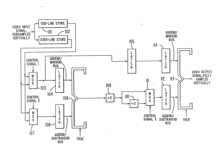
Referring to the drawing in the FIGURE 1 vertical
interpolator, the video input signal is subsampled n:l
vertically and can be subsampled p:1 horizontally. The
number n can be two or four, and p is a positive integer.
The successive lines of subsampled video in each frame are
consecutively ordinally numbered beginning with first in
order of their appearance. It is presumed that field
interlace is not used.
An odd-line line-storage memory 101 is loaded
with the first line of subsampled video input signal in a
time interval preceding the first scan line of video output
signal which is not subsampled vertically. An even-line
line-storage memory 102 is loaded with the second line of
subsampled video input signal in a time interval preceding
the second scan line of video output signal.
During each line trace interval of the video
output signal, line stores 101 and 102 are
non-destructively read from serially at the subsampling
rate of the video output signal of the FIGURE 1
interpolator. The odd-line store 101 is cyclically
reloaded a line at a time during each of a plurality of
~ 3 ~
-~- R~A 8~7~7/~727A
time windows with a successive one of the odd-nur~ered
lines of vertically subsampled video input signal.
Reloadings occur every 2nth line of the video output signal
of the FIGURE 1 apparatus, r~spectively, starting with a
time window be~ween the (n-l~th and (n-tl )th line trace
intervals of the video output signal of the FIGURE 1
interpolator.
The even-line store 102 is cyclically reloaded a
line at a time during each of a plurality of time windows
with a respective successive one of the even-numbered lines
of vertically subsampled video input signal. Reloadings
occur every 2nth line of the video output signal of the
FIGURE 1 interpolator, respectively, starting wi-th a time
window between the (2n-l)th and (2n+1)th line trace
intervals of the video output signal of the FIGURE 1
interpolator. These time windows are placed in a line
retrace interval, when the vertical interpolator is used in
the Sprague-Fedele-Ryan system.
Loading of line stores 101 and 10~ is done
serially, presuming them to be loaded from the serial port
of a VRAM. However, in other embodiments of the invention
line stores 101 and 102 are loaded parallelly, rather than
serially in time. Parallel-series loading arrangements can
also be implemented.
A multiplexer 103 coupled to the outputs of
stores 101 and 102 is operative to select the serial
read-out from one or the other of the line stores for data
latches 104 and 105. Latch 104 supplies the addend/minuend
bus of an adder/subtractor 106. Latch 105 aids in
compensating for phase delay between adder/subtractor 106
addend/minuend bus and its output terminal attendant upon
the use of phased logic.
A multiplexer 107 also coupled to the ou-tputs of
stores lO1 and 102 is operative to select the serial
read-out from one or the other of the line stores ~or a
data latch 108, which supplies the addend/subtrahend bus of
adder/subtractor 106. Adder/subtractor 106 is conditioned
by a TRUE control signal to operate as a subtractor
1 3 ~ Y~
-5- RCA 847Z7/84727A
supplying ~ difference signal owtput to a divide-by-two
circuit 109. The divided-by-two difference signal from
divide-by-two circuit 109 is applied to another
divide-by~two circuit 110 to generate a divided-by-four
difference signal. Divide-by-two circuits 109 and 110 each
typically consist of a simple shift of all bit places to
the next least significant bit places.
If the video input signal to line stores 101 and
102 is subsampled 2:1 vertically, a multiplexer 111
receives a first state of control signal (e.g., TRUE)
conditioning it to apply to a data latch 112 the
divided-by-two difference signal from divide-by-two circuit
109. If the video input signal to line stores 101 and 102
is subsampled 4:1 vertically, th~ multiplexer 111 control
signal alternates between the first state where the
divided-by-two difference signal is applied to latch 112
and a second state (FALSE if the first state be true) where
the divided-by-four difference signal is applied to latch
112.
Latch 112 supplies the addend/subtrahend bus of
an adder/subtractor 113, which is conditioned by a TRUE
control signal to operate as a subtractor. The
addend/minuend bus of adder/subtractor 113 is supplied from
a data latch 114 that receives delay-adjusted multiplexer
103 output signal from latch 105. The difference output
signal from adder/subtractor 113 is to be a video output
signal that is a replica of the original image data as
subsampled horizontally and fully sampled vertically. This
replica may contain error caused by the vertical
subsampling of the video input signal ~rom which it was
generated through interpolation.
FIGURE 2 tabulates the operation of the FIGURE 1
vertical interpolator when the video input signal is
subsampled 2:1 in the v~rtical direction. The video output
signal scan lines are consecutively numbered in the order
of their being scanned in the raster scan. The scan lines
in the subsampled set are denominated Ll, L2, L3, L4, L5,
L6, L7 et seq. with the consecutively numbered subscripts
~ 3 ~
-6- RCA 84727/~727A
denoting the order of their bei.ng scanned in the raster
scan. The line-store 101 and 102 contents are as described
above.
When the video output signal scan line
corresponds to a scan line in the 2:1 subsampled set, bo-th
multiplexers 103 and 107 select that subsample scan line --
from line-store 101, if the scan line be odd in the 2:1
subsample set, or from line-store 102, if the scan line be
even in the 2:1 subsample set. Whether multiplexer 111
selects to latch 112 one-half or one-quarter of the
subtractor 106 difference output signal is of no
consequence, since the minuend and subtrahend supplied
subtractor 106 are equal to each other to cause its
difference output signal to be zero-valued.
When the video output signal scan line is
half-way between two scan lines in the 2:1 subsampled set,
multiplexers 103 and 107 select outputs from diferent ones
of the line stores 101 and 102 for application to latches
104 and 108, respectively. The indications in the FIGURE 2
table that multiplexer 103 selection is opposite 107lS and
multiplexer 107 selection is opposite 103's refer to the
fact that multiplexers 103 and 107 select from opposite
ones of line stores 101 and 102. Multiplexer 111 is
conditioned by its control signal to select to latch 112
one-half of the subtractor 106 difference output signal.
For example, in the second scan line of the
output video signal, if multiplexers 103 and 107 select 2:1
subsample set scan lines L2 and L3 as minuend and
subtrahend respectively, for subtractor 106, its difference
output signal Ll - L2 is halved to generate (Ll - L2)/2
subtrahend signal for subtractor 113. Subtracting this
from its L2 minuend signal, subtractor 113 supplies as
difference output signal Ll - [~Ll - L2)/2] = (Ll/2) +
(L2/2). That is, 2:1 subsample set scan lines L2 and L3
are averaged to generate the second scan line of output
video signal.
FIGURE 3 tabulates the operation of the FIGURE 1
vertical interpolator when the video input signal is
~3~7~
-7- RCA 84727/~4727A
subsampled 4:1 in the vertical direction. The line store
101 and 102 contents are as described in the general
description of FIGURE 1.
Operation when the video ou-tput signal scan line
corresponds to a scan line in the 4:1 subsample set is the
same as when it corresponds to a scan line in the 2:1
subsample set. Operation when the output video signal scan
line is half-way between two scan lines in the 4:1
subsample set is the same as operation when it is half-way
between two scan lines in the 2:1 subsample set.
The other two spatial phases of vertical
interpolation from the 4:1 subsample set are of more
interest. Multiplexers 103 and 107 respectively select the
subsample scan lines closer to and further from the video
output signal scan line for respective application to
latches 104 and 108. Multiplexer 111 is conditioned by its
control signal to select to latch 112 one-quarter the
difference output signal of subtractor 106.
In the second scan line of output video signal,
for example, L1 is to be weighted by 3/4 and L2 is to be
weighted l/4. Multiplexer 103 selects L1 as being the 2:1
subsample set scan line closer to the output video signal
scan line, and multiplexer 107 selects L2 as being the 2:1
subsample set scan line further from the output video
signal scan line. ~ultiplexer 111 is conditioned by its
control signal to cause subtractox 106 difference output
signal ~L1 - L2) to be quartered in di~ide-by-two circuits
109 and 110. Subtractor 113 subtracts (L1 - L2)/4 from L1
to generate a difference output signal L1 - [(L1 L2)/4] =
(3L1/4) + (L2/4~-
In the fourth scan line of output video signal,
on the other hand, L2 is to be weighted by 3/4 and L1 is to
be weighted by l/4. Multiplexer 103 selects L2 as the
closer 2:1 subsample set scan line, and multiplexer 107
selects L1 as the further 2:1 subsample set scan line.
Subtractor 106 ~L2 - L1) difference output signal is
quartered in divide-by-two circuits 109 and 110, under
multiplexer 111 control. Subtractor 113 subtracts (L2 -
13~7.-~
-8- RCA 847Z7/847~7A
L1)/4 from L,2 to generate a difference ou~put signal L2 -
[(L2 - L1)/4] = (L1/4) -~ (3L2/4)
In the FIGURE 4 horizontal interpolator, the
video input signal, which may be the difference output
signal from the adder/subtractor 113 of the FIGURE 1
vertical interpolator, is subsampled p:1 horizontally,
where p can be two or four. This video input signal is
supplied to a divide-by-two circuit 121, which is usually
just a bit-place shifter. The half video input signal from
divide-by-two circuit 121 is supplied to another
divide-by-two circuit 122 to generate one quarter video
input signal. A multiplexer 123 selects either one-half or
one-quarter video input signal to a data latch 124 at the
addend/minuend input bus of an adder/subtractor 125
conditioned by a TRUE signal to operate as a subtractor.
At the beginning of a horizontal scan line of
video input signal samples, for a value of p e~ual to two,
multiplexer 123 selects one-half video input signal to
latch 124. A multiplexer 126 selects a ZER0 input signal
to a data latch 127 connected to the addend/subtrahend
input of adder/subtractor 125, so the difference output
signal is one-half the initial sample S1 of video input
signal. This half value S1/2 is applied to a data latch
128 supplying one of the two addend signals for an adder/
subtractor 129 conditioned by a FALSE signal to operate as
an adder. A multiplexer 130 selects this half value S1/2
to a data latch 131 supplying the other of the two addend
signals for adder 129. The sum output of adder 129 is -the
sum of the half values -- that is, the full value S1 of the
first video input signal sample in the scan line.
For the remainder of the scan line, whether p be
two or four, multiplexer 130 selects the sum output of
adder 129 to the latch 131. This provides for an
accumulation operation clocked at output sample rate. The
difference output signal from subtractor 125 will indicate
the amount of change from one pixel to the next, which is
to increment the adder 129 sum output. Consider now how
~ 3 ~
~9- ~CA 84727/847Z7A
this increment is calculated, first for p equal to two,
then for p equal to four.
If p equal t~o, multiplexer 123 selects one-half
video input signal to latch 124 throughout the scan line.
Multiplexer 126 selects the half-value initial sample Sl/2
to latch 127 to be subtracted in subtractor 125 from the
half-value second sample S2/~ clocked into latch 124.
Subtractor 125 supplies a difference output signal
(S2/2) - (Sl/2) to be accumulated over two ou-tput clock
cycles. The Sl output sample from adder 129 is incremented
by (S2/2) - (Sl/2) on the first output clock cycle to
generate the output sample Sl -~ [(S2/2) - (Sl/2)] = (Sl/2)
(S2/2). This output sample is incremented by (S2/2) -
(Sl/2) on the second clock cycle to generate the output
sample (Sl/2) + (S2/2) + [(S2/2) - (Sl/2)] = S2.
Multiplexer 126 then selects ZERO to latch 127, changing
subtractor 125 difference output signal to S2/2. The cycle
to generate the increment (S3/2) - (S2/2) then commences as
multiplexer 126 selects S2/2 to latch 127.
[(S3/2) - (S2/2)] will be accumulated the next two output
clock cycles. This general procedure of generating the
[S(k+l)/2) - (Sk/2)] increment at subtractor 125 output and
accumulating with it for two output clock cycles is
continued throughout the scan line with k taking successive
integral values.
If p equal four, multiplexer 123 selects
one-quarter video input signal to latch 124 throughout the
scan line. [(S(k+l)/4) - (Sk/4)] increment is calculated
similarly to the way [(S(k+l)/2) - (Sk/2)] was in the
preceding paragraph. This increment is accumulated for
four successive output cycles, rather than two, before the
next increment is calculated.
There are a variety of modes to initialize the
horizontal interpolator, for p equal to four, using
combinations of one-half and one-quarter of the first
sample. There are trade offs between the delay beore the
first valid sample occurs and clocking complexity. One
mode of operation of the FIG~RE 4 circuitry, for p equal to
-10 RCA 84727/84727A
four, will be descrlbed with reference to FIGURE 5. This
mode uses unal-tered clocking slgnals for the entire
horizontal line, including initialization.
Referring first to FIGURE 5, signals CLK 1 and
CLK 2 have frequencies equal to the outpuk pixel rate,
i.e., four times the inpu~ pixel rate. Signal CLK 2 is
delayed relative to signal CLK 1 and in the illustrated
example the delay is 90 degreesO It is presumed that
subtracter 125 and adder 129 of FIGURE 4 operate
synchronously with the signal CLK 1. In addition, latches
127 and 131 are respectively required to capture output
values from subtract~r 125 and adder 129 within the pixel
interval that they are produced. This is accommodated by
clocking latches 127 and 131 with clock signals which are
delayed with respect to the synchronous operation of the
adder and subtracter. The amount of phase delay is a
unction of the speed of the devices and the desired pixel
rate. One skilled in the art of circuit design will
establish this delay in accordance with the parameters of
the devices of choice and the pixel rate the system is
designed to pxoduce.
Latches 124, 127, 128 and 131 are assumed to be
"data" or "D-type" latches. Such a latch has a clock input
and responds to a transition at this input (assumed
positive), to load data which is at its data input terminal
immediately prior to the transition. Signals CLK 124, CLK
127, CLK 128 and CLK 131 are clock signals applied to the
clock input terminals of latches 124, 127, 128 and 131,
respectively. The clock signals are shown having narrow
pulses, but they may in fact be respective pulses of
signals CLK 1 and CLK 2 which are gated to the respective
circuit element at the appropriate time.
Also shown in FIGURE 5 is the data value in each
latch during each clock period as well as the output values
provided by subtracter 127 (i.e., DATA 1273 and adder 129.
Input pixel values A, B, C are the first three
pixel values of a compressed line of video signal and pixel
value A will nominally be the first pixel value of the
~ 3 ~
~11- RCA 84727/84727A
decompressed line of video signal. Immediately prior to
the application of input pixel value A (at the beginning of
each horiæontal line interval) the FIGURE 4 system is reset
so that the latches all contain zero values. In addition,
multiplexer 123 is conditioned to couple divider 122 to
latch 124 and multiplexer 130 is conditioned to couple the
output of adder 129 to latch 131. Multiplexers 123 and 130
are maintained in this state throughout each line interval
in this mode of operation.
At the first positive transition of signal CLK 1
(Tl) after input value A is applied, signal CLK 124 loads
the value A/4 into latch 124. Latch 127 contains a zero
(reset) value and thus subtracter 125 provides the value
A/4 at its output one clock period later (T2). CLK 124
loads a new value into latch 124 every pth cycle of signal
CLK 1 (Tl, T5, Tg).
One cycle after CLK 124 loads latch 124 (T2),
signal CLK 127, synchronous with signal CLK 2, and every
pth cycle of signal CLK 2 thereafter, loads a zero value
from multiplexer 126 into latch 127. After the first pulse
of signal CLK 127, latches 124 and 127 contain value A/4
and zero respectively. Thus on the next cycle of signal
CLK l (T3) subtracter 125 again provides the value A/4.
Multiplexer 126 then changes state and on the ne~t cycle of
signal CLK 2 (T3), and every pth cycle thereafter (T7, T11,
etc.), signal CLK 127 loads the output from subtracter 125
into latch 127, which value is held for three periods of
signal CLK 2.
After the first such pulse of signal CLK 127 (the
second pulse of CLK 127 illustrated in FIGURE 5) latch 127
contains the value A/4. Since latches 124 and 127 each
contain the value A/4 for this and the next subsequent
period of signal CLK 1 (T3, T4~ subtracter 125 will provide
an output value of zero for the two subsequent clock
periods (T4, T5).
The first pulse of signal CLK 128 occurs during
period T3 and subsequent pulses every pth period thereafter
at which times latch 128 is loaded with the output from
.~ 3 ~
-12- RCA 8~727/8~727A
subtracter 125. The values loaded into latch 128 are
equal to l/P times the quantity of the most current input
pixel value minus the previous input pixel value. Signal
CLK 131, having a pulse every period of signal CLK 2 loads
latch 131 with the previous output value provided by adder
129. At period T3 this value is egual to zero, hence at
period T4 the output of adder 129 is A/4. This value is
loaded into latch 131 during period T4 and is added to the
value A/4 provided by latch 128 to provide the value A/2 at
period T5 and so forth.
Subsequent output values provided by adder 129 at
intervals Ti, may be determined by summing the values in
latches 128 and 131 illustrated in FIGURE 5, that occur in
intervals Ti 1 The first valid interpolated output value
occurs during period T7 and all subsequent output values
are valid pixel values.
The FIC.URE 4 horizontal interpolator may be
modified by replacing divide-by-two circuit 121 with a
divide-by-four circuit. This will permit selec-tion between
horizontal interpolation to resample 4:1 horizontal
subsampling to full horizontal sampling and horizontal
interpolation to resample 8:1 horizontal subsampling to
full horizontal sampling. One skilled in the art and
equipped with the foregoing disclosure can readily design a
horizontal interpolator offering interpolation up from 2:1,
4:1 or 8:1 horizontal subsampling. Where 8:1 vertical
subsampling is to be used, it is preferable to do this
using line interlace on alternate fields and using the
FIGURE 1 interpolator in its 4:1 mode.
However, where progressive scanning is desired
together with 8:1 vertical subsampling this can be provided
for as follows. The input bus to the line stor~s 101 and
102 of FIGURE 1 is taken from a multiplexer that can select
between VRAM output and FIGURE 1 interpolator output. In
the line retrace interval just before the line trace
interval of a display scan line that is generated without
need for vertical interpolation ~rom a verticaLly
subsampled scan line, the line store holding the previous
~9~
-13- RCA 84727/24727A
vertically subsampled line is loaded with the succeeding
vertically subsampled line. In the next line retrace
interval the contents of the two line stores are weighted
by one half and added by the FIGURE 1 interpolator. This
sum is used to replace the contents of the line store
loaded during the previous line retrace interval in a
read-then-write operation. Other than loading the line
stores 101 and 102 differently, with interpolated lines in
the line retrace intervals flanking every fourth display
scan line line trace interval, the FIGURE 1 interpolator is
operated in its 4:1 mode.