Note: Descriptions are shown in the official language in which they were submitted.
13~6~
--1-
This invention relates to e:Lectrical circuits
for generating high magnitude electrostatic potentials,
and particularly to a system for driving a high voltage
transformer. ~he system utilizes a l~hase-lock technique
to drive th~ high voltage transformer at or near its
resonant frsquency. The invention is ~isclosed in the
context of high magnitude electrostatic potential
generating systems for use in electrostatically-aided
coating material application systems, such as liquid and
powder coating systems.
Industrial electrostatic coating systems
typically use high voltage direct current power supplies
to produce high magnitude potentials of up to 150
kilovolts (KV) DC across a pair of output terminals. One
of the terminals is generally held at or near ground
potential whlle the other terminal is held at a high
magnitude (typically negative) potential. The high
magnitude~potentla~l terminal~is coupled to a device that
charges particles~of the coating material as they are
~ dispensed.
Articles~to b~ coated are maintained~at a low
magnitude potential, typically at or~ near ground.` The
articles can be moved past the coating dispensing device,
f~or example, on a conveyor. The atomized~and charged
coatin~material moves through the electric field between
th~e~dispensing~device and the article. ~The charged~
coating material~ s;trikes the article~and sticks~to it.
The ~possi~ility of spark discharge between the
charging device and the articles~and other nearby
10~ ~ grounded;~rlrfaces Lreatas a conslderable hazard in
:.: ~....
::
.
:
:'
,
:
-2- ~3~8a
industrial electrostatic coating syst~ms. Certain
materials used in coating processes are volatile and
flammable. The desirability o a system which prevents
such spark discharge is apparent.
Spark discharges may occur when the potential
across the device-to-article space e~ceeds the dielectric
strength of the space, such as when the device and
article get too close to each other or when the magnitude
of the potential on the device i5 permitted to get too
1~ high. Typical electrostatic coating systems use
relatively large transformers operating at frequencies
well below the knee of the frequency response curve of
the transformer. In known electrostatic coating systems,
the transformer is selected so that the desired output
voltage taround 15 KV peak-to-peak~ is obtained in the
flat, linear range of the frequency r~sponse curve.
Changes in the operating conditions of the system, such
as when the operating freguency of the system varies, do
not affect the transformer output voltage unless the
operating fre~uency approaches the transformer resonant
frequency. As the operating frequency approaches the
transformer's resonant fre~uency, the voltage across the
transformer's output terminals can increase fairly
rapidly above the nominal voltage level, increasing the
2~ likelihood of a spark discharge.
Just prior;to spark discharge, an increase in
current across the high-magnitude potential terminals is
ordinarily noted. This current increase has been the
.
focus of much of the spark-discharge preYention equipment
in u~e today. See,~for e~ample, U~S. Paten~s: 3,851,618;
. ,
. .
~3~ 6~
3,875,892; 3,89~,272; 4,075,677; 4,1~7,527; and
4,402,030. It has also been noted, and use has been made
of the fact in the prior art, that if the stored energy
~ in the charging/dispensing device and associated circuit
components can be rapidly dissipated by this increase in
current that presages a spark discharge, such 3 discharge
can ordina;ily be averted. See, for egample, U.~. Patent
4,745,520. Other prior art which may be of interest
includes ~.S. Patents: 3,599,038; 3,608,823; 3,731,145;
4,16~,022, and 4,331,298.
Two common methods are used for powering a
transformer to drive the DC multiplier for generating
high DC potentials necessary to operate the charging
device. One method utilizes a self-sustaining power
oscillator designed to operate at the resonant frequency
of the transformer. The self-sustaining oscillator is
inefficient because it operates in class A. In addition,
under overload conditions, a self-sustaining system can
; double-mode or even cease oscillating. This causes the
design of fault protection circuitry to be difficult.
- ~ The second method utilizes a driven power
converter that forces the transformer-to operate at the
driven frequency. Even if the driven frequency is
initially adjusted to the transformer resonant frequency,
~significant changes occur in the transformer resonant
f~eque~cy due to circuit warmup and ambient temperature
effects. Tbe large number of transformer s~econdary
turns, the design and fabrication practices for high
voltage ~oils, and the nature of the DC multiplier load
;30 create a se~ondary circuit with a moderately high Q
.
,;
,'
.
. .
~1698~
64Q05-309
factor. Therefore, any shift in the frequency at which resonance
occurs can drastically alter circui~ performance.
It is an object of the present invention to provide an
electrostatically-aided coating dispensing system in which the
maximum outpuk voltage of the transformer provides the required
voltage to drive the charging device, thereby reducing the
likelihood that the transformer can be driven at a level at which
unwanted spark discharges are possible.
It is an object of the present invention to utilize a
high Q transformer driven at substantially its resonant fre~uency
so that the maximum voltage output of the ~ransformer is obtained.
It is an object of ~he presen~ invention to provide a
phase-locked loop to maintain the operating frequency of the
transformer substantially at its resonant frequency.
According to the present invention, there is provided in
~; combination, a high magnitude electrostatic potential supply, an
electrostatic potentlal utilization device, and means for coupling
the electrostatic potential supply to the utilization device, the
electrosta~ic potential supply comprising an operatlng potential
source, a transformer having primary and secondary windings, a
high potential rectifier and multiplier having a pair of output
termlnals, means for coupling the operating potential source to
the primary winding, means for coupling th~e secondary winding to
the high voltage rectifier and multipller, ~he circult including
the transformer and the high voltage rectifier and multiplier
~; ~ having a resonant frequency and a high Q, a phase comparator
having first and second inputs, a voltage controlled oscillator
::
.
, ~
,
,
: . , . . ~
1 3 ~
64005-309
having a free running frequ0ncy of substantially the transformer
resonant frequency, means for coupling the secondary winding to
the first input of the phase comparator, means for coupling the
output of the voltage controlled oscillator ~o the second input of
the phase comparator, means for driving the primary winding of the
transformer, means for coupling the driving means to the primary
winding, and means for coupling the voltage controlled oscillator
to the driving means to maintain the operating frequency of the
transformer substantially at the resonant frequency, variation of
the operating frequency from the resonant frequency rapidly
reducing the voltage across the output terminals of the high
voltage rectifier and multiplier.
Illustratively according to the inventlon, the phase
comparator controls the voltage controlled oscillator output such
that the signal f;rom the secondary winding and the~output signal
of the voltage controlled~oscillator are displaced in phase by
about 90 degrees. ~
~ Further, a~cording to the present invention, the mean~s
s~ for coupling the secondary winding to the phase comparator
comprises means for attenuating the voltage signal from the
secondary windlng.
Additionally,~according to the present invention, the
means~fo~r~ coupl~ing the phase~coDparator output to the voltage
; controlled oscillator input comprises a low pass filter.
; The invention may~best be understood hy referring to the
following~description~and~ the
S
~ A
: ~,
.. . .
'
.
.~ ~
`
-
~3~69~0
accompanying drawings which illustrate the invention. In
the drawings:
~ ig. 1 illustrates a simplified equivalent
circuit of a transformer which is used in the present
invention;
- Fig. 2a is a plst of the logarithm of the
~; magnitude of the ratio of output voltage to input voltage
versus the logarithm o~ frequency for a second order
system use^ful in understanding the present inYention; -
Fig. ~b is a plot of the phase angle between
output voltage and input voltage versus the logarithm of
frequency for a second order system;
Fig. 3 il~ustrates a block diagram of a system
constructed according to the present invention; and,
Fig. 4 illustrates a partly block and partly
schematic diagram of a system constructed according to
the present invention.
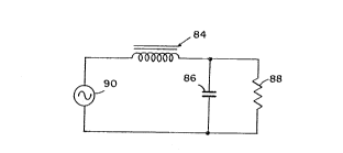
Fig. 1 illustrates a simplified equivalent
circuit for the transformer used in the present
invention. Because the transformer primary and secondary
~, ~ windings are wound on opposite legs of a double-U ferrite
core which maintains a nominal magnetic air gap, a
significant leakage reactance 84 exists between the two
: windings. The large number of seco~dary turns required
25 ~ to generate high voltage creates a large distributed
capacitance 86 across the second~ary winding, These two
reactive components;~84 and 86, along with the effective
load resistance 8~ comprise the passive elements of the
circuit of Fig. 1. The source voltage 90 is equal to the
transformer secondary-to-primary turns ratio times the
:
i
, ~,
' ";
, ~,, . ,, . . :
,, ~
" , . ~ ,. . .
voltage supplied to the primary winding. Although the
primary ~rive waveform is a square wave, the load voltage
is nearly sinusoidal because of operation at resonance.
The circuit of FigO 1 is a second order system
with the circuit Q factor determined by the effective
load resistance 88. Figs. 2a and 2~ illustrate the plots
of amplitude and phase of the ratio VOUt/Vin versus
~` frequency for such a high Q second order system.
Although both the amplitude and phase are functions of Q,
the phase curve passes through 90 degrees at resonance,
without regard for the value of Q. That is, resistive
loading does not alter the 90 degree phase shift at
resonance. The present system uses this 90 degree phase
shift characteristic at resonance to maximize system
15 ~ performance by maintaining circuit operation
substantially at transformer resonance.
'~ Fig.~3 illustrates in block diagram form an
electrical circuit for generating high magnitude
electrostatic potentials. The system includes a phase
~ ~ 20 comparator 110, a low pass filter 112, and a voltage
; ~ controlled oscillator (VCO) 114. The VCO 114 provides an
output signal to drive the primary winding of a
transformer 122. VCO 114 has a free running ~requency of
substantially the resonant frequency of transormer 122.
The output of VCO 114 is coupled to a divide by two
~ounter 116 to insure a 50 percent duty cycle waveform
for driving VMOS transistors 120-1 and 120-2 used to
drive transformer 122. ~This reduces the likelihood of
any saturation of the transformer 122 which might result
30 ~ from any waveform asymmetry.
~ .
,
13~g8~
--8--
The output of the divide by two counter 116 is
coupled to a driver 118 which buffers the drive waveforms
from VCO 114 and supplies the large peak cuxrent required
by the VMOS transistors 120-1 and 120-2. Transistors
120-1 and 120-2 are coupled to opposite ends of the
center-tapped primary winding of transformer 122. A high
voltage AC signal appears across the secondary winding of
transformer 122. The high voltage ~C signal across the
secondary winding of transformer 122 is coupled to a
multiplier 124 which rectifies and multiplies the AC
signal to produce the desired high magnitude DC output
voltage.
~ The high voltage AC signal from the secondary
; winding of transformer 122 is also coupled to an
attenuator 126. Attenuator 126 is coup}ed to one input
of phase comparator 110. The output of VC0 114 is
coupled to a second input of the phase comparator ~10.
~,
Phase comparator 110 compares the phases of the signals
from the atte~uator 126 and VC0 114 and qenerates a
20 ~ control signal~related to the phase difference. The
output o~ phase comparator 110 is coupled to a low pass
fi~lter 112 to provide a DC control voltage. The output
of low pass ilter 112 is coupled to the VC0 114 to ~;-
synchronize the output frequency of VCO 114 with the
2~ frequency from attenuator 126.
The VC0 114 operates initially at its free
running~freguency which is set to~substantiaIly the
; resonant frequency of the transformer 122. The control
signal ~rom the~phase comparator 110, a~ter passing
through~low pass filter 112, is appliad to the control
;,, .
.
::
~ 3 ~
g
terminal of VCO 114. The control voltage forces the VCO
114 output frequency to change in the direction which
increases or reduces to 90 the phase difference between
the signal from attenuator 126 and the VCO 114 output
signal. If the frequency from the attenuator 126 is
sufficiently close to the frequency of the VCO 114 output
~- signal, the phase-locked loop synchronizes the signal
from the VCO 114 with the signal from the attenuator 126.
~eferring now to Fig. 4, the phase comparator
110, low pass filter 112, and VCO 114 from Fig. 3 are
; included in a phase-locked loop integrated circuit 130.
A Circuit 130 illustratively is a National Semiconductor
type CD4046 CMOS integrated circuit. The pin numbers
illustrated in the drawing are those applicable when this
~ 15 ~ particular integrated circuit is employed for this
; ; purpose. This convention will be used when referring to
various integrated circuits described throughout this
detailed description. It should be understood that other
integrated circuits can be employed for the purposes for
which the various integrated cîrcuits describ~d herein
are used. ~ ~
The free running frequency of the VCO of circuit
130 is established~by the circuit on pins 6, 7 and 11 of
circuit 130. This circuit includes a .001 uF capacitor
132 coupled across pins 6 and 7 and a 15K resistor 134
coupled between pin 11 and ground. Pins 5 and 8 of
cir~uit 130 are coupled to ground, a~d pin 12 is coupled
through lM resistor 136 to groundO Pin 16 of circuit 130
~; is coupled to a +15 VDC supply voltage.~ Pin ~ of circuit
30~ 130, the output of the phase comparator, is coupled
t~ r l~
~ ,, ;.
,
-10- ~L3~9~
through the series combination o a lOOK resistor 138 and
a .1 uF capacitor 140 to ground. The common terminal of
resistor 138 and capacitor 140 is coupled the VCO input
terminal, pin 9 of circuit 130.
The output of the VCO, from pin 4 of circuit
130, is coupled to pin 3 of a D flip-flop integrated
circuit 116. Circuit 116 il~ustratively is a National
Semiconductor type CD4013 dual D flip-flop integrated
circuit. Pin 14 of circuit 116 is coupled to +15 VDC.
Pins 4, 6, 7, 8, 9, 10, and 11 of circuit 116 are coupled
to ground. Circuit 116 is connected in a divide by two
configuration.
The Q output from pin 1 of circuit 116 is
coupled to pin 2 of a driver integrated circuit 118.
Circuit 118 illustratively is a~Telsdyne type TSC426
integrated circuit. The Q output from pin 2 of circuit
116 is coupled to pin 4 of circuit 118. Pins 2 and 5 of
circuit 116 are coupled together. Pin 2 of circuit 116
is coupled to pin 3 of circuit 130 which is one input to
the phase comparator.
Pin 3 of circuit 118 is coupled to ground. Pin
6 of circuit 118 is coupled to ~15 VDC. Pin 7 of circuit
.,
118~is coupled ~o ~he cathode of a lN4746A zener diode
146. The anode of zener diode 146 is coupled to ground.
-~ 25 Pin 7 of integrated circuit 118 ;s also coupled to the
- ~ gate electrode of VMOS FET 120-1, Pin 5 of circuit 118
is coupled~to~he cathode of a lN4746A~zener diode 150,
and tAe anode;of zener diode 150~is coupled to ground.
Pin 5 of circuit 118~is also coupled to the gate
electrode of VMOS FET 120-2. FETs 120-1 and 120-2 are
- ; ~ illustratively International Rectifier type IRF520 FETs.
r o,~ rr\~r~
~:
.
3 ~
The source electrode of FET 120-1 is coupled to
ground, and the drain electrode of FET 120-1 is coupled
to terminal 154 of primary winding 156. The source
electrode of FET 120-2 is coupled to ground, and the
drain electrode of FET 120-2 is coupled to terminal 158
of primary winding 156.
Terminal 154 of primary winding 156 is coupled
to the anode of a lN6080 diode 160. The cathode of diode
160 is coupled to the cathode of a lN6080 diode 166 and
; 10 the anode of diode 166 is coupled to termînal 158 of
primary winding 156. The common terminal of diodes 160
and 166 is coupled to ground through the parallel
combination of a .01 uF capacitor 162 and a 15K resistor
164. The common terminal of diodes 160 and 166 is also
coupled to the cathode of a lN4754 zener diode 168. The
anode of diode 168 is coupled to ground. An operating
potential source is coupled to the center tap of primary
winding 156, and the center tap is coupled to ground
through a 47 uF capacitor 170.
The output signal from secondary winding 172 is -
a high voltage AC signal. The secondary winding 172 is
coupled to high voltage rectifier and multiplier 124
which provides a high voltage DC;output to drive an
electrostatic potential utilization device of any
25~ suitable type such as, for example, the type described in
U.S, Patent 4,198,932.
A high voltage sample from the secondary winding
S obtained by placlng a 1 ngth 177;of h1gh voltage wire
in close pro~imity to the transformer secondary winding
~; 30 172. This configuration appro~imates a 1 pF capacitor
.:
:: :
., '
~ 3 ~
-12-
176. It is understood that capacitor 176 which is
illustrated in broken lines is the effective capacitance
of the configuration of the length 177 of cable and
secondary 172.
The length 177 of high voltage wire is coupled
to ground through a .001 uF capacitor 178. Effective
capacitance 176 and capacitor 178 provide a 1000-to-1
high voltage attenuator 126. The distance of the
separatio~ of the high voltage wire from the secondary
winding 172 is determined by observation of the low
volt~ge sample from the attenuator 126. Because
: integrated circuit 130 has an extremely high input
impedance, the attenuator 126 preserves the phase
relationship.between the high voltage AC signal from
secondary winding 172 and the low voltage sample from the
attenuator 126. Because the transformer secondary
winding 172 operates around 15 KV peak-to-peak, the 15 V
:: peak-to-peak low voltage sample from the attenuator 126
provides a nearly optimum input level for circuit 130.
In place of length 177 of high voltage wire, a
~:: one- or two-turn winding on the secondary side of
: transformer 122 can be used to generate the hiyh voltage
sample which is fed back to integrated circuit 130.
The length 177 of high voltage wire is also
coupled through the series combination of a .01 uF
capacitor 180 and a lK resistor 182 to pin 14 of circuit
130. Resistor 182 is a current limiting resistor. Pin
14 of circuit 130 is an input to the phase comparator.
: Two types o phase comparators are included in
: 30~ circuit 130. A type I phase comparator tends to lock
,.
',',:
::
-13~
when its two inputs are displaced in phase by 90
degrees. Because a 90 degree phase shift e~ists between
the transformer primary and secondary windings 156 and
172 at resonance and no other phase shifts occur within
the circuit, the present system uses ths type I phase
eomparator. The phase comparator controls the VCO to run
at substantially transformer 122 resonant frequency.
The ma~imum output voltage of the secondary
winding provides the required voltage to operate the
charging device. Because the transformer has a high Q
value, any variation in frequency away from the resonant
frequency of the transformer will substantially reduce
the output voltage of the transformer. Therefore, the
risk of spark discharges caused by overdriving the
transformer is eliminated by the present invention.
Although the invention has been described in
detail with reference to a certain preferred embodiment,
variations and modifications exist within the scope and
spirit of the invention as described and defined in the
following claims.
.~
~ .