Note: Descriptions are shown in the official language in which they were submitted.
13~9~3~
~NEVEN SURFACE DATA DETECTION APPARATUS
BACKGROUND OF THE INVENTION
1. Field of the Invention
This invention relates to an apparatus for
detecting data of an uneven surface, such as human
fingerprint and the like, in a personnel identification
apparatus. More particularly, this invention relates to an
uneven surface data detection apparatus having a thin
structure.
2. Description of the Related Art
In today's high-tech world of information, a
strong demand has arisen for better computer system
security techniques. In particular, to protect
confidential data, a reliable identification must be made
of personnel in charge of such systems, and thus strict
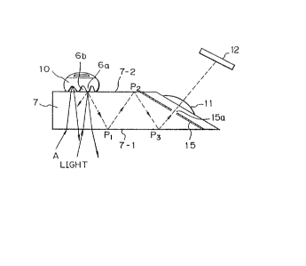
checks upon entrance to a computer room have become ver~
important. In the past, passwords and identification (ID)
cards have been used, and now personal identification
systems using fingerprints are increasingly used.
In a first conventional method for entering
uneven surface data te.g., a fingerprint), a fingerprint is
printed on paper using ink and is then sensed using an
image sensor. In this case, however, a finger must be
stained with ink each time the fingerprint data is to be
entered, and any uneven coating or blurring of the ink
greatly hinders the input operation.
In a se~ond conventional method, a light beam is
incident on a glass/air interface at a critical angle or
larger, and thus an uneven surface pattern is
instantaneously obtained. In this method, an uneven
surface data detection apparatus uses a prism. A finger
surface (uneven surface) pattern of a finger having
projections (ridges) and recesses (grooves) is pressed
against an oblique side portion of the prism, and light
from a light source is made incident on an obli~ue side
.,~
~ 31~33
-- 2 --
portion thereof at a critical angle or larger. The
incident light is scattered by the projections and is
totally reflected by the glass/air interface in the
recesses, and is then incident on a detector (e.g., an
imaging element), to thereby detect the uneven surface
pattern. Nevertheless, light leaks through an unclean
oblique surface caused by remaining fingerprints or
moisture, and this leakage light irradiates the recessed
portions of the fingerprint and is scattered. Therefore,
the level of the signal light from the projected portions
is lowered, and thus the contrast of the uneven surface
pattern is also lowered. Further, since a prism is used,
the total thickness of the apparatus cannot be reduced.
In a third known method (such as disclosed in
U.S. Patent No. 4,728,186), the apparatus includes a
transparent body made of glass or plastic and having a
lower surface and an upper surface parallel to each other,
and a diffraction grading including a lens. A finger
surface (uneven surface) pattern of a finger is pressed
against one of the surfaces, i.e., the upper surface, and
light is irradiated from the lower surface in a direction
substantially perpendicular to the transparent body. Air
layers exist in the recess of the finger, so that the light
which enters the recess i5 reflected at positions on the
surface of the recess and scattered in random directions.
Most of the light again enters the transparent base is
discharged from the other surface, at the same angle as the
light enters to the base. On the other hand, the light
which reaches the projections is scattered into the
transparent base, so that a part of the light is discharged
from the transparent base and the remaining is totally
reflected and transmitted through the transparent base.
The light reflected and transmitted through the transparent
base is derived from a diffraction grading and enters to an
image sensor, such as a CCD, in which an image of the
A
13~ 33
fingerprint can be obtained.
In the known finyerprint detection apparatuses
discussed above, the optical elements, such as an image
sensor, a diffraction grating, or the like, must be located
opposite to and spaced from the fingerprint contact
surface, and therefore, a relatively large space is
required for obtaining the image data of the fingerprint.
That is, an apparatus known in the prior art must have a
relatively large thickness, and this makes it difficult to
incorporate such a fingerprint detection apparatus in a
door, a keyboard of computer terminals or the like.
SUMMARY OF THE INVENTION
A feature of one embodiment of the present
invention is to pxovide an uneven surface data detection
apparatus, such as a fingerprint detection apparatus,
having a relatively thin thickness, so that such an
apparatus can be easily incorporated in a door, a keyboard
of computer terminals or the like.
A feature of another embodiment of the present
invention is to provide an uneven surface data detection
apparatus, capable of overcoming the disadvantages
mentioned above with reference to the related or prior art.
According to the present invention, there is
provided an uneven surface data detection apparatus for
detecting an uneven surface having projected portions and
recessed portions, comprising: a transparent base having
first and second surfaces, at least a part of said first
surface defining an uneven surface contact portion; a light
source for illuminating said uneven surface on said uneven
surface contact portion, said light source simultaneously
illuminating said projected portions and recessed portions
of said uneven surface, so that the light derived from the
recessed portions enters to the transparent base and comes
out thereof,
_ 4 - ~31~3~
and at least a part of the light derived from the
projected portions is totally reflected at least one
time by the second surface opposite to said first
surface; a focussing lens integrally formed on or
integrally adhered to said transparent base, said
focussing lens being located at a position for drawing
said totally reflected light out of said txansparent
base; and an image sensor arranged outside of said
transparent base for detectins an image of said uneven
surface including said projected and recessed portions.
In the present invention, the focussing lens is
integrally formed on or integrally adhered to the
transparent base. Therefore, a thickness of this
apparatus including an optical system can be reduced,
and thus it is possible to incorporate such an apparatus
in a door, a keyboard of computer terminals or the like.
The focussing lens comprises a convex lens. The
apparatus preferably comprises: an iris diaphragm
having an aperture, said iris diaphragm being arranged
in such a manner that said aperture is located at a
position corresponding to a center of the curvature of
the radius of said convex lens, so that the light can be
totally reflected at an area of said aperture. Such a
total reflection preventing means may comprise a metal
plate arranged in or adhered to said transparent base.
Alternatively, such a total reflection preventing means
may comprise a metal film formed by a vapor depositing
of a metal, a rough surface r or a light absorbing paint
film coated on said transparent base.
In one embodiment of this invention, said
collimator lens comprises a cylindrical portion having
one end integrally connected to said transparent base
and the other end integrally formed with a convex lens
portion.
In another embodiment, said transparent base has a
third surface inclined to said first and second surfaces
and said third surface is formed as a mirror surface, so
_ 5 - ~3~ ~33
that the light once totally reflectad by said second
surface is reflected by said mixror surface in such a
manner that a propagation direction of the light
reflected by said mirror surface is directed
substantially parallel to said first and second
surfacesO
In further embodiment, said apparatus further
comprises a light shield box accommodating said image
sensor, said shield box comprising a wall, a part of
said wall being defined by said iris diaphragm. The
total reflection preventing means comprises a metal
plate adhered to said transparent base and said convex
lens is adhered to said metal plate from the inside of
said light shield box, in such a manner that said convex
lens is integrally connected to said transparent base
through said aperture. In still another embodiment,
said apparatus further comprises a prism or second lens
between said prism and said image sensor. The object to
be detected may be a human finger having a fingerprint
and said apparatus further comprises a guide member
provided on said irst surface for guiding the finger on
said uneven surface contact portion, said guide member
being incorporated wi~h said light source, so that the
light illuminates the uneven surface through said
finger.
In the typical embodiments, the first and second
surfaces of the transparent base are parallel to each
other. However, in fact, the first and second surfaces
are not always necessary to be parallel to each other,
but the only necessity is that the light from the
projected portions or ridges must be at least once
totally reflected by the second, opposite surface.
BRIEF DESCRIPTION OF THE DRAWINGS
Figure 1 is a schematic side view illustrating a
principle of the structure of an uneven surface data
(fingerprint) detection apparatus of this invention;
Figure 2 is a side view of an embodiment of this
. - 6 ~ ~31~3
invention;
Figure 3 is a schematic view illustrating an
operation of an optical system in the embodiment shown
in Figs. 1 and 2;
Figure 4 is a view of the optical system shown in
Fig. 3;
Figure 5 is a diagram illustrating a position of
the image determined by a calculation;
Figure 6 is a schematic side view illustrating an
embodiment of a total reflection preventing means having
an aperture;
Figure 7 is a schematic view of a door providing
therein with a fingerprint detection apparatus of this
invention;
Figure 8 is a perspective view of a computer
keyboard on which a fingerprint detection apparatus of
this invention is mounted;
Figure 9 is a side view of another embodiment of an
optical system of a fingerprint detection apparatus of
this invention;
Figure 10 shows still another structure of a
fingerprint detection apparatus of this invention;
Figure 11 is a side view of an embodiment of a
transparent body used in a fingerprint detection
apparatus of this invention;
Figure 12 is a side view of another transparent
body used in a fingerprint detection apparatus o this
invention;
Figures 13, 14, and 15 are views of respective
embodiments of the optical systems of this invention
using a prism;
Figure 16 is a schematic cross-sectional view
illustrating a principle structure of a further
embodiment of a fingerprint detection apparatus of this
invention;
Figure 17 is a cross-sectional view illu~trating in
detail the embodiment of khe fingerprint detection
3 3
apparatus shown in Fig. 16;
Figures 18 and 1~ are top and perspective views
of a guide member used in the embodiment shown in Fig. 17;
Figure 20 i5 a cross-sectional view of an
embodiment of a fingerprint detection apparatus which is
also intended for use as an optical living body detecting
apparatus; and
Figures 21 and 22 are schematic views
illustrating uneven surface data detection apparatuses
known in the prior art.
DESCRIPTION OF THE PREFERRED EMBODIMENTS
Referring initially to Figures 21 and 22, these
figures illustrate uneven surface data detection
apparatuses known in the prior art.
In one conventional method, a light beam is
incident on a glass/air interface at a critical angle or
larger, and thus an uneven surface pattern is
instantaneously obtained. In this method, as illustrated
in Fig. 21, an uneven surface data detection apparatus uses
a prism 2, a finger surface (uneven surface) pattern of a
finger 1 having projections (ridges) 6a and recesses
(grooves) 6b is pressed against an oblique side portion of
the prism 2, and light from a light source 3 is made
incident on an oblique side portion thereof at a critical
angle or larger. The incident light is scattered by the
projections 6a and is totally reflected by the glass/air
interface in the recesses 6b, and is then incident on a
detector (e.g., an imaging element) 4, to thereby detect
the uneven surface pattern. Nevertheless, light leaks
through an unclean oblique surface caused by remaining
fingerprints or moisture, and this leakage light irradiates
the recessed portions 6b of the fingerprint and is
scattered. Therefore, the level of the signal light from
,~
~ 3 ~ 3 ~
- 7a -
the projected portions 6a is lowered, and thus the contrast
of the uneven surface pattern is also lowered. Further,
since a prism is used, the total thickness of the apparatus
cannot be reduced.
In another known method, such as illustrated in
Figure 22 (and disclosed such as in U.S. Patent No.
4,728,186), the apparatus includes a transparent body 7
made of glass or plastic and having a lower surface 7-1 and
an upper surface 7-2 parallel to each other, and a
diffraction grading 8 including a lens. A finger surface
(uneven surface) pattern of a finger is pressed against one
of the surfaces, i.e., the upper surface 7-2, and light is
irradiated from the lower surface 7-1 in a direction
substantially perpendicular to the transparent body 7. Air
layers exist in the recess 6b of the finger, so that the
light which enters the recess 6b is reflected at positions
on the surface of the recess 6b and scattered in random
directions. Most of the light again enters the transparent
base 7 is discharged from the other surface 7-1, at the
same angle as the light enters to the base 7. On the other
hand, the light which reaches the projections 6a is
scattered into the transparent base 7, so that a part of
the light is discharged from the transparent base 7 as
shown at R2, and the remaining is totally reflected and
transmitted through the transparent base 7 as shown at R3.
The light R3 is derived from the diffraction grading 8 and
enters to an image sensor 4, such as a CCD, in which an
image of the fingerprint can be obtained.
A basic principle of an uneven surface data
detection apparatus according to the present invention will
now be described with initial reference to Fig. 1. An
object having an uneven surface, such as a human finger 10,
is pressed against a transparent or light transmission base
13~9~3~
- 7b -
7 (e.g., glass) having a lower surface 7-1 and an upper
surface 7-2 which are substantially parallel to each other.
In Fig. 1, projected portions (ridges) 6a and recessed
portions (grooves) 6b, which constitutP a fingerprint of
the finger 10 are emphasized. As can be seen from the
drawing, the projected portions 6a are in contact with the
upper surface 7-2, and the recessed portions 6b are
separated from the upper surface 7-2 so that an air layer
is formed between the recessed portions 6b and the upper
surface 7-2. Light is radiated to the transparent base 7
from the lower surface side 7-1 thereof, as indicated by
arrows A, and light entering the interior of the base 7 is
randomly reflected by the projected portions 6a and is
thereby scattered in all directions, since an air layer is
not formed at the projected portions 6a. Scattered light
beams which satisfy the total reflection condition of the
base 7 (i.e., have an angle larger than a critical angle)
are totally reflected by the lower surface 7-1 (at P1) of
the base 7, as indicated by the dashed line in Fig. 1,
1 3 ~
-- 8 --
totally reflected by the upper surface 7-2 (P2) thereof,
totally reflected again by the lower surface 7-1 (at P3)
thereof, and pass thxough a focussing lens 11 to be
de~ected by an image sensor 12 arranged ou~side of the
transparent base 7.
On the other hand, at the recessed portions 6b,
light passes through out of the base 7, since an air
layer is formed thereat. The light beams which reach
the recessed portions 6b of finger 10 are randomly
reflected by the surfaces of the recessed portions 6b,
and are converted into scattered light. This scattered
light again enters the base 7 from the upper surface 7-2
thereof and then externally discharged from the lower
surface 7-1 of the base 7 at the same angle as the
incident angle thereof, in accordance with Snell's law
(as indicated by the solid line). Therefore, the
scattered light from the recessed portions 6b is no
longer transmitted through the interior of the base 7.
Accordingly, only the totally reflected light
transmitted through the interior of the base 7 is
detected by the image sensor 12 to obtain an uneven
surface pattern imageO
Thus, the projection data and the recess data are
discriminated depending on whether or not an air layer
is formed between the transparent base 7 and the
finger 10, since all the light components scattered by
the recessed portions 6b are discharged outside the
base 7 as indicated by the solid lines. On the other
hand, the light components propagating through the
interior of the base 7 correspond to the data from the
projected portions 6a and must be detected only to
obtain uneven surface pattern data with a good contrast.
~ he light components propagate through the interior
of the base 7 and reach a position corresponding to the
collimator lens 11 which is integrally formed on or
integrally adhered to an inclined surface o~ the
transparent base 7. Since the total reflection
g ~ 3 3
condition can be no longer satisfied at this position,
the light components are guided through the focussing
lens 11 and externally from the transparent base 7, and
thus the pattern data from the light components of the
projec~ion 6a is then detected by the image sensor 12.
A charge coupled device tCCD), such as SONY CORP.,
018-L, can be advantageously used as such an image
sensor 12.
In Fig. 1, the reference numeral 15 denotes an iris
diaphragm 15 having an aperture 15a. The transparent
base 7 can be made of any transparent or light
transmissible material, such as glass or plastic. The
image sensor 12 is arranged so that an input surface
thereof is inclined to the propagation direction of the
light entering the image sensor 12, to minimize
aberration.
Figure 2 illustrates an embodiment of this
invention, wherein a focussing lens 11 mounted on an
inclined surface of the transparent base 7 comprises a
cylindrical portion 13 having one end integrally
connected to the transparent base 7 and the other end
integrally formed with a convex lens portion 14. An
iris diaphragm 15 having an opening aperture 15a is
advantageously formed on the inclined surface of the
transparent base 7 in such a manner that the
aperture 15a is located at a position corresponding to a
center of curvature of the radius of the convex lens
portion 14, and thus the aperture 15a is positioned at a
connecting portion between the transparent base 7 and
the focussing lens 11.
In Fig. 2, the light discharged from the focussing
lens 11 is reflected by a mirror 16 arranged outside of
the transparent base 7 and then enters to the image
sensor 12. In Fig. 2, when the finger 10 i5 placed on
the uneven surface detection portion on the upper
surface 7-2 of the transparent base 7, the light
scattered by the projected portions 6a of the
- 10 - ~ 3 3 9 ~ ~ 3
fingerprint is transmitted as shown by a dotted line and
totally reflected at points P1, P2, and P3 in turn,
focussed by the lens 11, and then reflected by the
mirror 16.
Figure 3 illustrates a straight optical path in the
embodiment of Fig. 1 and Fig. 2. To simply explain the
optical path of the light passing through the points P1,
P2, and P3, and the mirror 16, the transparent base 7
can be shown as it is assumed to be developed along the
scattered light path, under the condition that a
straight light from the projection portions 6a of the
fingerprint is assumed as an optical axis. Since one of
the surfaces of the base 7, i.e., the upper surface 7-2
(the fingerprint detection surface), is inclined to the
optical axis, it is understood that an input surface of
the image sensor 12 also must be inclined.
It should be necessary to locate the opening
aperture 15a at a position corresponding to a center of
the cur~ature radius of the convex lens, due to a
remarkable aberration which arises when focussing the
light beam by a convex lens. In face, since the
fingerprint input surface is inclined to the optical
axis and, therefore, the length and breadth ratio of a
fingerprint image is changed depending on the focal
distance of the lens, it is necessary to take the change
into consideration when dealing with the data input the
image sensor 12.
Figure 4 is diagrammatical view of the optical
system shown in Fig. 3 and illustrates the relationship
between the fingerprint input surface and the image
sensor surface, wherein the optical system uses a
semi-spherical lens having a curvature radius r. In
Fig. 4, assuming that an original point O is the center
of the curvature radius r of the lens; the direction of
the optical axis is z; the direction of the iris
diaphragm providing with the opening aperture 15 is y;
and the direction perpendicular to the ~-axis and z-axis
11 - 13~ ~33
and perpendicular to the sheet, is x, then B refers to a
point on the projected portions on the fingerprint input
surface (finger contact surface) and located on an
extension of the z axis; the distance ~1 of BO is 90 mm;
the distances of AB and BC are 10 mm, respectively; the
refractive index of the transparent base 7 is 1.5; and
the curvature radius r is 10 mm.
Figure 5 illustrates the results of calculation for
the change of the image obtained on the sensor surface.
According to ~ig. 5, the distance L2 of OB~ is about
37.5 mm, and although the original position (flat
surface) of the image is as indicated by the dashed
line, the image according to the results of the
calculation is as indicated by the solid line including
points A', B~ and C'. At the point B', the image îs
deviated in the direction of Z-axis by 200 ~ or less.
Nevertheless, such a small deviation falls within a
focal depth of the lens, so that the whole fingerprint
of a single finger can be entirely focused on the sensor
surface by a single spherical convex lens.
Figure 6 illustrates an embodiment of the total
reflection preventing means (iris diaphragm) 22 having
the opening aperture 22a. A thickness of the
transparent base 7 is selected in such a manner that the
center P of curvature radius of the convex lens 11 is
located ~ust on one of surfaces (i.e., the lower
surface 7-1) opposite to the fingerprint detection
portion on the upper surface 7-2) of the transparent
base 7, and an oblique aperture 22a (the area where the
total reflection preventing film is not formed) is
formed on a total reflection preventing film 22.
Therefore, the light incident to the area of the oblique
aperture is totally reflected. On the other hand, the
light incident to the outside area of the oblique
aperture cannot be reflected and is absorbed by the film
portion. The reason why the aperture should have an
oblique-shape is that ~he optical beam is inclined with
- 12 ~ 3~
respect to the reflection surface. Of course, such an
oblique aperture operates in the same manner as the
circular-shaped opening aperture in a general optical
system.
Figure 7 illustrates an example which uses an
uneven surface (fingerprint) data detection apparatus
according to the present invention. Where personnel
entrance control should be conducted by identifying the
fingerprints of individual persons, it is preferable to
situate a fingerprint data detection apparatus in a
door, particularly to completely insert it within the
region defined by a thickness of the door, to attain
both an easy operation and a preferred appearance. As
shown in Fig. 7, a transparent base 7 is made in such a
manner that a part thereof is bent and buried in the
door 17 in the vicinity of the knob 18. The optical
system for entering fingerprint image data to the image
sensor 12 thus can be arranged as shown without
affecting the appearance of the door 17. To conduct the
entrance control, all that is necessary is to place a
finger on the fingerprint contact surface of the
transparent base 7 of the door. In Fig. 7, the same
reference numerals indicate the same parts as in the
embodiments as mentioned abo~e.
Figure 8 illustrates another application example
which uses a fingerprint data detection apparatus of
this invention to identify a person able to access a
data base in a computer system. In this case, it is
preferable not to provide an independent fingerprint
data input apparatus, but to incorporate a fingerprint
data input apparatus in a keyboard, to obtain both an
easy operation and a preferred appearance. In the
example shown in Fig. 8, reference numeral 19 indicates
a keyboard and reference numeral 20 indicates a terminal
apparatus of the computer.
Figure 9 is a side view of another embodiment of an
optical system of a fingerprint detection apparatus of
- 13 - ~3~
this inventionJ wherein the ligh~ from ~h0 fingerprint
contact surface 7-2 is once totally reflected by the
lower surface 7-1 and then reflected by a mirror 24
formed on an inclined end face of ~he transparent
body 7, so that the light reflected by the mirror 24
becomes substantially parallel to the upper fingerprint
contact surface 7-2 and to the lower surface 7-1 o~ the
transparent body 7, and passes therethrough to the
semi~spherical lens 14, which can be adhered to the
other end face of the transparent body 7. Also~ the
opening aperture 15a of the iris diaphragm 15 is
positioned a~ the center of curvature of the radius of
the semi-spherical lens 14.
Figure 10 shows still another structure of a
fingerprint detection apparatus of this invention. In
this embodiment, the light from the fingerprint contac~
surface 7-2 is once totally reflected by the opposi~e
surface 7-1 and then reflected by a mirror 24 formed on
the inclined face of the transparent body 7, in the same
manner as in the embodiment of Fig. 9.
A metal plate 25 having an aperture 15a is adhered
by a suitable optical adhesion to the other end face of
the transparent body 7, i.e., to the surface S
perpendicular to ~, in such a manner that the
aperture 15a is positioned on L. Here, L is defined as
an optical axis of the light transmitted from the
fingerprint contact surface 7-2 and reflected by the
mirror 24.
A lens having a cylindrical portion 13 and a convex
lens portion 14 similar to the lens shown in Fig. 2 is
adhered by a suitable optical adhesion to the metal
wall 25 from the opposite side of the transparent
body 7, so that the center of curvature radius of the
convex lens portion 14, is positioned at the
aperture 15a.
An optical magnetical shield box 30 has an open end
and accommodates therein the image sen~or 12~ such as a
- 14 ~ ~319~3~
CCD moun~ed on a printed circuit substrate 31. A shi~ld
box 30 is integrally connected to the metal plate 25 in
such a manner that the opened end of the shield box 30
is closed by the metal plate 25 and the light receiving
surface of the sensor 12 is inclined by a certain angle
to the optical axis L. ~ signal fxom the image
sensor 12 is externally output from the shield box 30 by
a cable 32.
Since the image sensor 12 is optically opened to
the outside through only a very small pin-hole, i.e.,
the aperture 15, the shield box 30 is completely
shielded or closed, and thus magnetic influences or
unfavorable light affec~ing the image sensor 12 can be
effectively avoided.
Figure 11 illustrates an embodiment of a
transparent body 7 used in a fingerprint detection
apparatus of this invention. In this embodiment~ the
transparent body 7 has a rough surface 15 inclined by
45 with respect to the finger contact surface 7-2, so
that the transparent body 7 has a substantially L-shaped
configuration. The surface 15 has a smooth portion
which defines an aperture lSa positioned at the center
of curvature of the radius of the focussing lens 14.
The rough surface 15 prevents the total reflection, but
absorbs the light incident thereon. On the other hand,
the aperture 15a allows a total reflection, and
therefore, the light the finger contact surface 7-2 is
totally reflected by the opposite surface 7-1 at Pl, by
the surface 7-2 at P2, by the surface 7-1 at P3, and
then by the inclined surface at lSa, since the light
incident on the rough area 15 is scattered and does not
enter the focussing lens 14, and only the light incidant
on khe smooth area (i.e., the aperture) 15a is totally
reflected and enters the image sensor 12 through the
focussing lens 14.
Figure 12 illustrates another transparent body,
wherein the transparent body 7, is bent twice by 90
_ 15 - ~3~ 3
into a substankially J-shaped configuration. Thak is,
the transparent body 7 has a first total reflection (or
mirror) surface 7-3 inclined by 45 with respect to the
finger contact surface 7-2, a successive second total
reflection surface 7-4 inclined by 45 to ~he first
total reflection surface 7-3, an opposite total
reflection surface 7-5 parallel to the second
surface 7-4, and a rough surface 15 inclined by 45 to
the third surface 7-3.
In the above embodiments, the to~al reflection
preventing means may be constituted by either one of a
metal plate, a metal film formed by, e.g., vaporde-
position, a rough surface, a light absorbing paint film,
or the like.
Thus the surface 15 has a smooth portion which
de~ines an aperture 15a positioned at the center of
curvature of the radius of the focussing lens 14.
Therefore, the light from the finger contact surface 7-2
is totally reflec~ed by the opposite surface 7-1 at Pl,
~ by the surface 7-3 at P2, by the surface 7-5 at P3, by
the surface 7-4 at P4, again by the surface 7-5 at P5,
and then by the inclined surface at 15a. The light
enters to the rough area 15 is scattered and does not
enter the focussing lens 14, and only the light input to
the smooth area (i.e., the aperture) 15a is totally
reflected and enters the focussing lens 14 and is
focussed on the image sensor 12.
Figures 13, 14, and 15 illustrate embodiments of
the fingerprint detection apparatus, particularly an
optical system using a prism. ~he embodiment shown in
Fig. 13 is similar to that of Fig. 9, except that a
prism 26 is arranged between the focussing lens 14 and
the image sensor in such a manner that the optical
length of a light path incident on the image sensor 12
becomes uniform in the whole region of the fingerprint
image. Thereforef the image obtained on the sensing
surface of the image sensor 12 has less aberrations or
- 6 - ~3~ ~33
distortions.
The embodiment shown in Fig. 14 is similar to tha~
of Fig. 13, except that a second lens 27 is further
arranged between the prism 26 and the image sensor 12 in
such a manner that the light corrected by ~he prism 26
is further focussed by the this lens 27 and enters to
the image sensor 12.
In the embodiment shown in Fig. 15, a prism
portion 28 is incorporated in the transparent hase 7.
~his prism portion 28 has a refraction index n2 which is
larger than a refraction index n1 of the transparent
base 7. Therefore, the light (which comes from the
fingerprint contact surface 7-2 and is at least once
totally reflected by the lower surface 7-1) is corrected
before being focussed by the focussing lens 14, in such
a manner that the length of light path becomes uniform
in the whole region of the fingerprint image.
Therefore, the image obtained on the sensing surface of
the image sensor 12 has less aberrations or distortions.
Figures 16 to 20 are views illustrating a further
embodiment of a fingerprint detection apparatus of this
invention. If the object to be detected and having an
uneven surface having pro~ected portions and recessed
portions is transparent, or at least partially ligh~
transmissible, and has a light scattering surface ~a
human finger is such an object), a light source for
illuminating the uneven surface can be located at the
side of upper surface of the transparent body 7, as
shown in Fig. 16. In this case, the uneven surface is
illuminated by the light transmitted through the
object (finger) itself, so that a part of the light can
be discharged from the projected portions (P) and the
rest can be discharged from the recessed portions (Q),
in the same manner as in the previous embodiments.
In Figs. 17, 18 and 19, a substantially U-shaped
guide member 41 is provided on the upper fingerprint
contact surface 7-2 of the transparent base 7. The
~3~33
guide member 41 has a guide openin~ 42 in which a
finger 10 is inserted. Since the U-shaped guide
member 41 is fixed to the upper surface 7-~ of ~he
transparent base 7, when a finger is inserted in the
guide opening 42, the fingerprint comes into contact
with the surface 7~2 at a predetermined position. A
pair of light sources 43, such as laser diodes or LED,
small lamps or the like, are inserted and fixed in a
pair of recesses 44 as shown in Fig~ 17. Each of the
recesses 44 is preferably communicated with a
cone-shaped opening 46, to widen the illuminating region
toward the inside of the U-shaped guide member 41. A
pair of or a plurality of paixs of such light sources 43
may be provided. Laser diode or LED arrays 45, as shown
in Fig. 19 also can be used. Thus the fingerprint on
the contact surface 7-2 is uniformly illuminated by the
light coming from the respective sides of the U-shaped
guide member 41 and passing through the finger itself.
The light used in this embodiment is preferably selected
so that the light has a certain wavelength to show a
high light transmissible characteristics.
In Fig. 20, the U-shaped guide member 41 is
incorporated with a pair of light emitting elements 43,
such as ~ED's as mentioned above, and a light receiving
element 48. The light emitted from the light emitting
elements 43 passes through the finger placed on the
fingerprint contact surface 7 2 and is received by the
light receiving element 48. A part of the light emitted
from the light emitting elements 43 illuminates the
fingerprint through the finger itself. As is well
known, a condition of the blood, such as a distribution
of the red blood corpuscles of a part of a human body,
such as a finger, is subjected to periodical changes due
to blood pulsation. Thus the amplitude of the light
received by the light receiving element 48 is also
periodically changed, and therefore, if a human finger
is correctly placed on this apparatus, this can be
~ 3 ~ 3
de~ected before the detection of a finger print. Thus
if the light receiving element 48 receives a certain
periodically changing amplitude of the ligh~, it can be
considered that a human finger i5 correctly inserted to
the guide member 41, and thereafter, the detection of a
fingerprint can be started.
For example, if a finger is incorrectly inserted,
such as inserted while wearing a glove, or if an other
article is inserted to the guide member 41, such a
periodically changing amplitude of the light cannot be
received by the light receiving element 48. In this
case, a detection of a fingerprink can not be started.
U.S.. Patent NoO 4,728,186 discloses a personal
identification system, such as a system for discrim-
inating detected data and the registered databeforehand, and the same ystem can be used here~