Note: Descriptions are shown in the official language in which they were submitted.
. 22184
~3~73~
FREQUENCY MODULATION BALLAST CIRCUIT
TECHNICAL FIELD
The present invention relates to ballast .
circuits for gaseous discharge lamps and, in
particular, to a ballast circuit utilizing frequency
modulation to start and control the operation of
fluorescent lamps while maximizing the life of the
lamp electrodes.
~.
.. ~................................................................... :
.
.
2 ~3~7~
BAC~GROUN3 OF THE INVENTION
A fluorescent lamp is basically a glass tube
filled with a gas, such as a combination of neon and
a small amount of mercury vapor. The interior of the
tube is coated with a phosphorus material and each
end of the tube includes a filament cathode and an
anode structure. In operation, each end of the tube
is alternately the anode or the cathode during one
half of the alternating current cycle.
When a high voltage, on the order of several
hundred volts, is established between the two ends of
the lamp, the gas within the tube becomes ionized and
forms a conduction path, thereby producing an
electric arc through the gas. After the gas is
ionized and an arc is formed, the lamp has an
extremely low electrical resistance. The electric
current passing through the lamp produces energized
molecules and electrons which strike the phosphorus
material which then produces light that is emitted
from the tube.
During operation of the lamp, the anode serves
as the collector for charged ions. Heat is generated
at the anode by the bombardment of arriving ions on
the anode. The amount of heat generated by the
arriving ions is determined by the relative anode
voltage and the length of time the anode is
positively charged. Thus, low frequency alternating
current, such as standard 60 hertz, causes the anode
to collect ions from a great distance because it is
positively charged for a relatively long time. The
ions accelerate toward the anode during the entire
half cycle, and the ions farthest from the anode
arrive at relatively high velocities, imparting
!
~....
.
.~
'~ ~
: .
7 3 ~
significant mechanical energy to the anode. The
energy of ion bombardment causes heating and erosion
of the anode. The erosion of the anode is a major
factor affecting the lifetime of the lamp and a major
limitation to the maximum light intensity that can be
obtained from a given fluorescent lamp.
The power and the lifetime of a fluorescent lamp
are affected by the frequency of the alternating
current and the shape, or ~crest factor~, of the
alternating current waveform. In any given waveform
there is a peak voltage and an averaye voltage.
Although a certain minimum voltage is necessary to
operate a fluorescent lamp, the ideal waveorm is a
square wave, which has the lowest ratio of peak to
average voltage, or the lowest crest factor. The
square wave produces the highest average current with
the least amount of anode erosion caused by high peak
voltage. Other waveforms can provide the same
average current, but with an undesirable high peak
voltage that produces a current pulse during the
cycle. During the current pulse, ions arrive at the
anode with greater energy, causing rapid erosion of
the electrodes and limiting power and efficiency of
the lamp.
Z5 Prior art ballast circuits have not been
designed to maximize the lifetime of fluorescent lamp
electrodes in operations involving either low power
dimming or high light intensity. Prior ballast
circuits generally provide an undesirable
distribution of output energy with respect to time,
either in the waveform shape, the time intervals
between voltage pulses, or both. Ballast circuits
¦ which provide for lamp dimming by increasing the time
4 ~ 7 3 ~
period between high power voltage pulses cause
disproportionate anode erosion in relation to the low
light intensity produced. Ballast circuits which
provide for lamp dimming by changing the waveform shape
of a fixed Prequency alternating current produce a high
crest factor which causes disproportionate electrode
erosion during the high power pulse, thereby limiting
the li~e of the lamp and the usable dimming range.
In general, prior art ballast circuits do not
provide for optimum lamp life in either dimming
operations or high intensity operations. Therefore,
there is a need for a fluorescent lamp ballast circuit
which provides extended lamp lifetime by minimizing
electrode erosion during lamp start-up, dimming
operations, and high intensity operations.
C.
:
5 13~7~
SUMMARY OF THE INVENTION
The ballast circuit of ~he present invention
utilizes frequency modulation for starting and
operating fluorescent lamps while maximizing the
lifetime of the lamp electrodes. Frequency
modulation allows both dimming operations and high
intensity operations without causing disporportionate
erosion of the anodes due to ion bombardment. The
development of high intensity fluorescent lamps
having a long lifetime makes it practical to use
fluorescent lamps as the source of light for high
speed optical scanning devices.
The ballast circuit of the present invention
utilizes a half-bridge output circuit to drive an
inductor/capacitor (LC) tank circuit tuned to the
minimum operating frequency of the lamp. The lamp
driver circuit produces a sinusoidal waveform at the
lowest operating frequency, which i5 the condition of
maximum current flow to the lamp due to the
inductance of the choke. ~n oscillator circuit
provides a frequency modulated square wave output to
modulate the frequency of the driver power to control
the light output of the lamp. For example, at
maximum power the lamp may operate at about 50 k~z,
and at minimum power the lamp might operate at 200
k~z, holding the lamp to 1/4 of the maximum power.
Fluorescent lamps start easier at higher
frequencies. The ballast circuit of the present
invention switches to its highest frequency to start
the lamp and switches to a lower operating frequency
after the lamp has started. Thus, the present
invention allows a lower voltage start-up that
minimizes erosion of the electrodes, eases the power
6 ~31~7~
surge in the circuit, and improves the reliability of
the power supply.
Another aspect of the ballast circuit of the
present invention is a photodetector feedback loop
which includes a photoresistor to monitor the light
output of the lamp. The photoresistor circuit is
coupled to the oscillator circuit to provide feedback
for automatic starting and direct control of the lamp
and to compensate for decay of the lamp with age.
The circuit may also include a second sensor to
respond to commands, events, or ambient conditions in
a remote location. In addition, the control circuit
will accept an analog voltage signal from a computer
to set the light level, which can be detected and
maintained by the photoresistor feedback loop.
When the photoresistor detects that there is no
light output from the fluorescent lamp, the driver
circuit switches to the start-up mode. During start-
up, there may be a short time delay during which low
frequency, high current power is provided to quickly
heat the lamp electrodes. Following this short
delay, the driver circuit automatically switches to
the high frequency, low voltage start-up signal to
establish the arc across the lamp.
The ballast circuit may include an idle mode
which, when activated, drives the fluorescent lamp to
the high frequency, minimum power level. The idle
mode allows the lamp to remain activated at a very
low power level and permits it to be driven quickly
to the maximum power level.
The present invention also allows the use of two
to three times greater power than is used in a
conventional fluorescent lamp without causing
:
'
:
7 ~3~ ~ j7s~
excessive erosion of the electrodes. Such high
intensity fluorescent lamps may be used in high speed
optical scanning operations. In the past, high speed
optical scanning utilized tungsten lights for
illumination. However, tungsten lights produce intense
heat which can ignite or damage the articles being
scanned if they stop or become jammed under the light.
The use of fluorescent lamps with the ballast circuit of
the present invention provides sufficient high intensity
light for high speed optical scanners without the
generation of excessive heat.
The present invention is applicable to any type of
gas discharge lamps including fluorescent and mercury
vapor lamps.
In accordance with one aspect of the invention
there is provided a ballast circuit for a gas discharge
lamp, comprising: a direct current power source; means
for producing a variable frequency control signal; means
responsive to said control signal for producing a
switched output from said direct current power source,
said switchsd output having a frequency proportional to
said control signal; and an inductor connected to
provide said switched output to drive said lamps wherein
greater power is supplied to said lamps when the
freguency of said control signal is decreased and less
power is supplied to said lamp when the frequency of
said control signal is increased.
8 ~3~7~
BRIEF ~ESCRIPTION OF THE DRAWINGS
For a more complete understanding of the present
invention and for further advantages thereof,
reference is now made to the following Description of
the Preferred Embodiments taken in conjunction with
the accompanying Drawings, in which:
FIGURE l is a schematic diagram of the
oscillator/detector circuit of the present invention;
FIGURE 2 is a schematic diagram of the power
output circuit of the present invention;
FIGURE 3 is a schematic diagr~m of an optional
detector circuit of the present invention showing a
remote light sensor;
FIGURE 4 is a schematic diagram of an alternate
circuit for detecting the illumination status of the
lamps; and
FIGURE 5 is a schematic diagram of an alternate
power output circuit utilizing direct lamp
coupling.
9 ~3~ ~7
lll
DESCRIPTION OF T~E PREFERRED EMBODIMENTS .
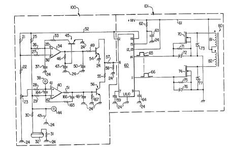
FIGURE 1 is a schematic illustration of a
photodetector feedback circuit 100 connected to an i
oscillator circuit 101. Reference numeral 60
indicates an integrated circuit power supply control
chip that has been configured to operate with a
constant full pulse width and to modulate only the
operating frequency of its output. For example, chip
60 may comprise a UC3524A integrated circuit chip
which is manufactured by Unitrode. The reference
numerals within the block representing the chip 60
indicate the various terminal pins of the chip.
The multifunction control chip 60 performs the
following functions: a) Chip 60 provides a 5-volt
precision reference at pin 16 that is used to power a
line 52 and to provide reference voltages in the
serially connected string of resistors 21, 22, and
23; b) Chip 60 incorporates an oscillator, the
frequency of which is determined by a capacitor S9
connected to pin 7 and by the current drain at pin 6
provided by the detector circuit 100; and c) Chip 60
provides frequency modulated square wave output
waveforms 65 and 66 at pins 11 and 14 which are 180
out of phase with each other.
Power from an 18-volt bus 61 is fed directly to
pins 12 and 13 of chip 60 to provide full potential
for the square wave output circuitry. Reference
numeral 24, which is used throughout the FIGURES,
indicates a common 18-volt return bus. Pin 15 is the
power input terminal for the internal logic circuitry
of chip 60. The input voltage to pin 15 is
conditioned by resistor 62 and capacitor 63, which
insulate pin 15 from bus noise generated by the
1 0
square wave output circuit~ A 5-volt reference from
pin 16 is applied to pin 2 to disable the pulse width
modulation function and to obtain maximum pulse width
for full duty cycles at all times. Pin 16 is further
connected to a line 52. The input signals to chip 60
consist of those from capacitor 59 attached between
pin 7 and return bus 24 and those from the current
drain of the detector circuit 100 attached to pin
6. The value of the current drain, or cumulative
resistance of the detector circuit 100, determines
the output freguency of chip 60 at pins 11 and 14,
the lower the resistance at pin 6, the higher the
frequency of the output. Capacitor 64, which is
connected between pin 9 and return bus 24, bufEers
the error output circuitry of chip 60 so that the
response of chip 60 to frequency changes is not
erratic.
In the detector circuit 100 of FIGURE 1, a
photoresistor 32 is positioned to detect the light
output of fluorescent lamps 126 and 127, which are
shown in FIGU~E 2. The resistance of photoresistor
32 varies from less than one hundred ohms to several
megohms. The string of resistors 21, 22, and 23 is
fed from the 5-volt reference pin 16 of chip 60
through line 52. The junctions between resistors 21,
22, and 23 provide reference voltages at the
inverting input 36 of an operational amplifier 34 and
at the non-inverting input 41 of an operational
amplifier 40. The values of the resistors 21, 22,
and 23 are determined by the power levels necessary
for the fluorescent lamps to start and operate.
Operational amplifier 34 controls the lamp starting
conditions and operational amplifier 40 controls the
.
11 ~3~7~
lamp operating conditions. Resistors 26, 27, 28, and
29 are input resistors to operational amplifiers 34
and 40. A second set of resistors 25, 30, and 31 are
serially connected with photoresistor 32 to provide
voltage control for photoresistor 32. Resistor 25
limits the photoresistor current to safe levels.
Resistors 30 and 31 serve to isolate ~he detector
circuit 100 from any noise generated by the circuit
link to photoresistor 32.
When the fluorescent lamps 126 and 127 are
operating at usable light levels, the photoresistor
32 pre~ents a resistance of approximately 50 to 5000
ohms. With the photoresistor 32 in this condition,
the voltage at non-inverting input 35 is lower than
the voltage at inverting input 36, which causes
operational amplifier 34 to have a low output to
buffer resistor 49 and capacitor 50, thereby turning
off transistor 54. Thus, the lamp starting circuit,
comprising operational amplifier 34 and transistor
54, is held inactive by providing a high impedance to
pin 6.
The operational amplifier 40 is configured as a
voltage comparator and acts to minimize any voltage
differential between non-inverting input 41 and
inverting input 42. The voltage at input 41, which
determines the light level of the fluorescent lamps
126 and 127, is adjusted by the wiper setting of the
variable resistor 23. The circuit comprising
operational amplifier 40, buffer resistors 51 and
167, capacitors 48 and 164, an RC network consisting
of resistor 165 and capacitor 166, a transistor 56,
and photoresistor 32 functions as part of a feedback
circuit to control the intensity of the light output
12 ~ 3~7~
produced by fluorescent lamps 126 and 127. For
example, if the voltage at input 42, which is
determined by the photoresistor 32, is less than the
reference voltage at input 41, which indicates that
the lamp intensity is grea~er than that selected by
the wiper at variable resistor 23, the output of
operational amplifier 40 will increase, thereby
turning on transistor 56 to a degree dependent on the
voltage differential between inputs 41 and 42. ~s a
1~ result, the current flow from pin 6 of chip 60 will
increase, thereby raising the output frequency of
chip 60 as explained above.
Resistor 58 establishes the minimum operating
frequency of the chip 60, which in this embodiment is
55 kHz. With transistor 56 switched on fully, the
current drain from pin 6 through resistors 55 and 57
increases to drive the chip 60 to its maximum
operating frequency, which in this embodiment is
approximately 155 kHz. Thus, if lamp brightness
increases, the resistance of photoresistor 32
decreases, lowering the voltage level at input 42 and
raising the output of operational amplifier 40, which
in turn increases the current from pin 6 through
transistor 56. This action causes the output
frequency of chip 60 to increase, which reduces the
current to the fluorescent lamps 126 and 127, as
described below, and returns the light level to
equilibrium. The detector circuit 100 of this
invention is capable of regulating the light
intensity of the lamps to within ~1% of the selected
level.
When the fluorescent lamps 126 and 127 are off
and the photoresistor 32 is dark, the resistance of
" , ' . . ' ~
.
13 ~3:~7~
the photoresistor 32 is very high compared to the
other resistors in the circuit. In this state, the
voltage at input 35 is higher than the voltage at
input 36, which causes operational amplifier 34 to
S have a high output. The high output from operational
amplifier 34 turns on transistor 54 which effectively
shorts out transistor 56 and resistor 55 and drives
the chip 60 to its highest frequency, which is now
determined only by resistors 57 and 58. This start-
up freguency, greater than 350 kHz, is higher than
the normal steady state operating frequencies for the
lamps. However, when the lamps start and illuminate
photoresistor 32, the resistance of photoresistor 32
drops significantly and brings the voltage at input
35 to below that of input 36, thereby turning off
operational amplifier 34 and transistor 54 and
returning control to operational amplifier 40.
The function of operational amplifier 34 is
modified by capacitor 37 to enhance electrode heating
during the lamp starting cycle. Capacitor 37 is in a
discharged state prior to initiation of the start-up
cycle. When the start-up cycle is initiated,
capacitor 37 begins to charge, which momentarily
holds the voltage at input 35 at a low level. This
action delays the turn-on of operational amplifier 34
so that operational amplifier 40 will operate the
lamp driver circuit 200 of FIGURE 2 at a low
frequency and provide extra current to heat lamp
electrodes 131, 132, 133, and 134, shown in FIGURE 2,
prior to the start-up attempt. When capacitor 37 is
completely charged, operational amplifier 3~ and
transistor 54 turn on and activate the high frequency
starting conditions. When the lamps start, control
. - ~ ,.
,
14 ~3~ ~73~
of lamp operation returns to operational amplifier 40
as explained above.
If the lamps fail to start on the first attempt,
the high output of operational amplifier 34 will
charge capacitor 47 through resistor 46 and turn on
transistor 45, which will discharge capacitor 37
through resistor 33. As a result, the low frequency
electrode warming cycle will be resumed until
capacitor 37 is once again fully charged and
operational amplifier 34 and transistor 54 are again
turned on to reactivate the starting frequency. This
sequence will be repeated until the lamps start
successfully.
The circuit of FIGURE 1 also has provisions for
an external override of the operating conditions. ~n
idle condition can be caused by closing switch 43 or
by applying a ground state to jack 44. In either of
these conditions, the output of operational amplifier
40 will go high and increase the oscillator frequency
of chip 60 to its highest operating frequency,
thereby minimizing power output to the lamps. Jack
44 may be used, for example, to idle the lamps
between demand periods, to sense external events, or
to permit computer control of light exposure times.
Jack 38 is provided to receive an external
voltage signal to imposs a remotely controlled level
of light intensity. The remotely controlled light
level could be in response to ambient lighting
conditions, a remote event, or an external computer
3~ control signal. An example of an ambient light
circuit connected at jack 38 is illustrated and
described below in conjunction with FIGURE 3.
~.~ .
: , ,
.
15 ~3~7~
As shown in FIGURE 1, oscillator chip 60
provides square wave outputs 65 and 66 at pins 11 and
14. When the output at pin 14 goes high, a field
effect transistor 70 switches on and applies current
to a winding 81 of a transformer 80. Zener diode 72
ensures that the voltage applied to the gate of
transistor 70 does not exceed 20 volts. When the
voltage at pin 14 goes to zero, resistor 71 ~unctions
to discharge the gate of transistor 70, thereby
turning off transistor 70. Zener diode 73 ensures
that the voltage across transistor 70 does not exceed
its maximum rating.
A short period of dead time will occur after the
voltage on pin 14 goes low and before the voltage on
pin 11 goes high. When the voltage on pin 11 goes
high, a transistor 74 switches on and applies current
through a winding 82 of transformer 80. The primary
windings 81 and 82 of transformer 80 are configured
so that the decay of winding 81, as transformer 70 is
2~ switched off, adds to the total primary transformer
current. The function of the circuit components 75,
76, and 77 associated with transistor 74 are
identical to those associated with transistor 70 and
described above. Further, it is anticipated that
more specialized integrated circuits can be used to
replace chip 60 and provide the power to drive
transformer 80 directly so as to eliminate the need
for transistors 70 and 74.
The power output circuit 200 of the present
invention is illustrated in FIGURE 2. Secondary
windings 104 and 105 of transformer 80 are configured
such that the power output of each winding is 180
out of phase with the other. As a result, a
'
.
, ~ . ' ,
1~ ~3~ ~73~
transistor 108, a high voltage field effect
transistor, switches on when a similar transis~or 109
switches off, and transistor 109 switches on when
transistor 108 switches off. The waveforms applied
at the gates of transistors 108 and 109 are square in
shape, thereby optimizing the efficiency of
transistors 108 and 109.
Ferrite beads 106 and 107 suppress voltage
spikes and ringing conditions on the gate leads of
transistors lOB and 109, respectively. Diodes 112
and 113 act to protect transistors 108 and 109,
respectively, from high inverse voltages. Capacitor
161 and resistor 162 act to suppress radio frequency
noise on the output circuit generated by the dead
time between switching of transistors 108 and 109.
Three RF filters 95, 96, and 97 remove radio
frequency interference from the input power lines 91
and 92 and protect transistors 108 and 109 from
voltage transients. Diodes 93 and 9~ function with
capacitors 98 and 102 to provide a voltage doubler
and direct current source, with resis~ors 99 and 103
acting as bleeder resistors. With 110 volts AC at
input lines 91 and 92, 155 volts DC is present across
each of the capacitors 98 and 102.
When transistor 108 switches on due to positive
voltage on its gate, current is drawn from the
capacitor 98, upward through a primary winding 121 of
a transformer 120, through an inductor 114 and
transistor 108, and returned to the capacitor 98,
thereby charging capacitor 115 so that the terminal
; of capacitor 115 joining trans~ormer 120 is
positively charged.
,. .
.. .
17 ~3~
When the voltage across the transformer B0
reverses, transistor 108 switches off and transistor
109 switches on. In this phase of operation, current
is drawn from the capacitor 102, through transistor
S 109 and inductor 114, and downward through winding
121 of transformer 120, thereby reversing the charge
of capacitor 115 so that the terminal of capacitor
115 joining transformer 120 is negatively charged.
Inductor 11~ is connected at the common output
of the two power transistors 108 and 109. Induc~or
114 and capacitor 115 are selected so that at the
lowest operating frequency, which provides the
highest power to the lamps 126 and 127, the wav0form
produced by transistors 10~ and 109 is a sinusoid.
This waveform provides the maximum power with the
lowest ratio of peak voltage to average voltage,
thereby minimizing erosion of the lamp anodes.
During operation of lamps 126 and 127, control
of starting and intensity is provided by the
frequency modulated output of chip 60. As the
operating frequency increases, the reactance of
inductor 114 also increases, thereby reducing the
amount of current passing through the primary winding
121 of transformer 120 and reducing the power
provided to lamps 126 and 127. Therefore, as the
operating frequency of the driver circuit 200
increases, the amount of power transferred to the
fluorescent lamps 126 and 127 decreases.
Although two fluorescent lamps are shown in
FIGURE 2, the circuit 200 could also be used to drive
a single lamp or any other type of gas discharge
lamp, such as a mercury vapor lamp.
.
.
.i ~
18 ~3~ ~3i~
Inductor 114, capaci~or 115, and transformer 120
comprise an inductive/capacitive tank circuit which
is resonant at a certain frequency and which uses
capacitors 98 and 102 as alternate power sources in a
half-bridge fashion. The operation of the present
invention, however, is not limited to the use of a
half-bridge output circuit since any series output
circuit capable o~ being driven at variable
frequencies would be functional according to the
principles of the invention.
The actual electrical ratings of inductor 114,
capacitor 115, and transformer 120 are selected to
match the lamp driver circuit 200 to the specific
type of lamp being used and to the relative power
lS levels required. The reactance of inductor 114 is
selected to pass a desired amount of current at the
lowest operating frequency. The reactance of
capacitor 115 is selected to provide a sinusoidal
waveform at or near the lowest operating frequency.
2Q The primary and secondary windings of transformer 120
are configured to properly drive the selected lamps
in the desired power range. The secondary windings
123, 124, and 125 of transformer 120 are utilized to
heat the electrodes 131, 132, 133, and 134 of lamps
126 and 127.
FIGURE 3 illustrates an optional detector
circuit 300 which may be connected to jack 38~ A
resistor 141 serves to limit the maximum current
available to a remote photoresistor 145. ~esistors
143 and 144 serve to isolate the circuit 300 from any
noise generated by the components associated with
photoresistor 145. A variable resistor 142
establishes the light level setting desired at the
~ . . ..
~L3~73~
remote photoresistor 145. The voltage established at
resistor 142 is combined with the voltage established
at resistor 23 to determine the actual voltage
applied at input 41, which determines the light level
setting. The resistor 146 can be varied to establish
the relative response of the system to light level
changes at the remote photoresistor 145. For
example, a large value of resistor 146 would require
a greater excursion of the light level at
photoresistor 145 to change the output of operational
amplifier 40.
FIGURE 4 illustrates a current sensing circuit
400 for determining the operational status of lamps
126 and 127. Circuit 400 is a variation of the power
output circuit 200 shown in FIGURE 2 together with a
portion of the oscillator/detector circuit 100 shown
in FIGURE 1, wherein like reference numerals identify
similar circuit elements. In this alternate circuit
400, input 35 of amplifier 34 is connected to the
reference voltage at line 52 through resistor 26.
This connection tends to hold input 35 high with
respect to input 36, which simulates the voltage
relationship between inputs 35 and 36 when the lamp
detector photoresistor 32 of FIGURE 1 is dark.
FIGURE 4 also illustrates the addition of a
diode 168 in the base circuit of transis~or 45. The
addition of this diode does not affect the starting
cycle sequence described in reference to FIGURE 1. A
resistor 16g serves to isolate the lamp current
sensing circuitry from the base circuit of transistor
45 until the lamps are started. The starting cycle
sequence described in reference to FIGURE 1 performs
in the same manner for circuit 400. In circuit 400,
. .~ .
.
~ 3 ~
the output of operational amplifier 34 is determined
by the level of current detected flowing through
lamps 126 and 127. A current sensing transformer 155
is inserted in th~ circuit 200 of FIGURE 2 at point A
in series with the high voltage secondary winding 122
of transformer 120. When lamps 126 and 127 are not
ignited, a capacitor 153 is discharged by a resistor
152, such that the operation of transistor 45 and
operational amplifier 34 is not affected. As a
result, the high frequency starting signal is
supplied as described above. The cyclic starting
attempts also described above in reference to ~IGURE
1 remain the same.
When lamps 126 and 127 are started, capacitor
153 is charged through diode 154. Zener diode 151
functions to limit the maximum voltage during current
transients and a resistor 152 functions to discharge
capacitor 153 when the lamp driver circuit of the
present invention is turned off. When capacitor 153
is charged to a minimum voltage level necessary to
turn on trannsistor 45 through resistor 169, input 35
is forced low and the output of operational amplifier
34 is turned off, thereby turning off transistor 54
and transferring control to operational amplifier 40
as described above. Diode 168 serves to isolate the
low output of amplifier 34 from the elevated base of
transistor 45.
An economical version of the present invention
utilizing a direct coupled output to the lamps is
illustrated as circuit 500 in FIGURE 5. In its basic
configuration the circuit achieves high frequency
starting, idle, and current control without light
detectors, such as photoresistor 32. The degree of
3 ~
21
light regulation can be changed if lamp temperatures
change. However, ballast circuit jacks 38 and 44 and
~witches ~3 and 172 permit precision external
regulation if needed.
A direct coupled power output configuration is
illustrated in FIGURE 5 for circuit 500. The function
of the circuit 500 is identical to the power output
circuit 200 illustrated in FIGURE 2. The output power
transformer 120 has been removed and the tank circuit
inductor 114 and capacitor 115 are coupled directly to
the electrodes 131 of lamp 126 and 134 OI lamp 127
respectively.
Transformer 156 serves only as a filament
transformer with winding 157 a~ a primary winding.
Output windings 158, 159 and 160 are equivalent in
function to the windings 123, 124 and 125 of the
tran~former 120 shown in FIGURE 2.
The radio ~re~uency snubber network comprising
resistor 162 and capacitor 161 remains the same for
both output configurations.
Transf~rmer 155 and the associated circuitry
consisting of diode 154, capacitor 153, resistor 152
and zener diode 151 function as described in
reference to FIGURE 4. The operation of operational
amplifier 34 is the same as that described in
reference to FIGURE 4. However, the output of
transformer 155 is now used both to start the lamps
126 and 127 and to regulate the lamps when switch 170
is closed to position 171. When switch 170 is closed
to position 171 and the power transistors 108 and 109
are alternately switched on, transformer 156 provides
filament power, but no current will flow through
current transformer 155. A resistor 173 holds
~, ~
. .
22 ~ 73~
operational amplifier input 41 low. The reference
voltage at line 52 holds inputs 35 and 42 high
respectively. Operational amplifier 40 then has a
low output, thereby providing the lowest frequency
power to warm t~e filaments of the lamps 126 and
127. Operational amplifier 34 will be held low
momentarily due to the charging of capacitor 37.
When capacitor 37 charges, amplifier 34 will generate
a high output, initiating the starting cycle as
described in FIGURE 1.
When the lamps strike, current flows from return
bus 24 through resistors 173 and 174 to transformer
155. Current drawn from the base of transistor ~5
through resistor 169 turns on transistor 45 which
pulls down input 35 of amplifier 34, turning off
transistor 54, thereby stopping the start sequence
and yielding control to amplifier 40. If the voltage
at input 41 of amplifier 40 climbs above that of
input 42, indicating high lamp current, amplifier 40
increases its output, turning on transistor 56 which
will increase the lamp driver frequency at the output
of transistors 108 and 109 and reduce the lamp
current until inputs 41 and 42 are at equilibrium.
The actual lamp current level is adjusted by the
voltage at the wiper of resistor 23. This
configuration provides lamp regulation based on lamp
current alone. Jack 44 and switch 43 can be used to
force an idle condition by grounding input 42 of
amplifier 40. With input 42 at ground and input 41
at some operational level, amplifier 40 increases its
output, turning transistor 56 on and driving the lamp
driver transistors 108 and 109 to maximum operating
frequency, until the ground condition is removed.
~`
23 ~ 7 3 ~
Jack 3B is not effective with switch 170 in
position 171.
When switch 170 is in position 172, transformer
155 is used only to determine lamp ignition status as
is shown in FIGURE 4. The precision voltage at line
52 provides a reference voltage to input 41 of
amplifier 40 through the series of resistors 173 and
174. The voltage applied to input 41 is suficiently
positive to exceed any voltage available at the wiper
of resistor 23. With input 41 held higher than input
42~ amplifier 40 has a high output, turning on
transistor 56 and driving the lamp driver circuit of
the present invention to its highest frequency or
idle condition.
When switch 170 is in position 172, the lamp
driver c$rcuit of the present invention will remain
in the idle condition until reduced voltages are
applied to jack 38. This can be accomplished by any
method including those previously identified above.
The precision of regulation is determined by the
voltage at jack 38. The remote detector circuit 300
illustrated in FIGURE 3, for example, will function
in this configuration.
Although the presen~ invention has been
-described with respect to specific preferred
embodiments thereof, various changes and
modifications may be suggested to one skilled in the
art, and it is intended that the present invention
encompass such changes and modifications as fall
within the scope of the appended claims.
' ' `, '
: