Note: Descriptions are shown in the official language in which they were submitted.
-- 20 1 4376
BACKGROUND OF THE INVENTION
This invention concems an electronic power supply for driving an electroacoustictransducer at its resonant ultrasonic frequency, typically a predetermined frequency in the
range between 18 kHz and 60 kHz. More specifically, this invention refers to a power
supply for driving a piezoelectric transducer provided with a horn at its parallel resonant
frequency, such transducer and hom cor"binalion being used most frequently for welding
thermoplastic parts, requiring power from ssveral hundred watts to several kilowatts for
time intervals ranging from several milliseconds to a few seconds. A typical prior art
power supply of this type is shown in U.S. Patent No. 3,432,691 issued to A. Shoh, dated
March 11, 1969, entitled "Oscillatory Circuit for Electroacoustic Converter". The power
supply disclosed hereafter incorporates improvements and novel features not present in
the prior art supply, such features being necessitated by the requirement that ultrasonic
welding apparatus be operable by computer control at high speed and under conditions of
high precision and repeatability involving varying workpieces and production runs.
- 201437~
SUMMARY OF FEATURES OF THE INVENTION
The present invention discloses a power supply for driving a piezoelectric
transducer provided with a horn at its parallel resonant frequency, typically 20 kHz,
wherein the amplitude of mechanical vibrations manifest at the output surface of the
horn can be adjusted and retained constant at the adjusted value, wherein the
starting sequence, that is bringing the transducer with horn from standing still to its
full vibrational amplitude, is effected in a fast and stepless manner, wherein the
resonant frequency of the transducer and horn combination is tracked and used as a
control signal to adjust the frequency of the power supply, wherein the flow of
current to and from the transducer is limited to preset values, and, finally, including
means for accomodating higher rates of operation (weld cycles) than has been
possible with the prior art devices.
The following description will provide an overview of the novel features
indicated above.
Amplitude Adjustment
Ultrasonic transducers for power applications normally are operated in their
parallel resonant mode. By the use of a compensation inductor, the power supply
will act as a voltage source. With suitable tuning, the amplitude of mechanical
vibration manifest at the transducer output surface is then proportional to the drive
voltage (motional voltage) and the value of the current is proportional to the power
demanded by the workpiece. In this manner, the amplitude of vibration can more
easily be regulated or adjusted despite wide variations in power requirements.
20~ 4376
Most known power supply designs utilize a two part circuit to acco""~lish
v;l.ralion amplHude adjustment. (This is apart from the use of mechanical booster
homs or horns of di~rerenl mechanical gain coupled to the transducer assembly for
amplitude adjustment). The major component of the power supply is a converter
circuit employing electrical switching devices for converting direct current voltage to
an aller, lalillg current voltage whose frequency is dictated by the mechanical
resonance of the ultrasonic transducer. The amplitude of the alternating currentvoltage is governed by the value of the direct current voltage supplied to the
switching devices and hence, the amplitude of the vibration is a function of the direct
current voltage amplitude. For changing the amplitude of vibration, the value of the
direct current voltage must be changed. The direct current voltage is derived byrectifying and filtering the alternating current line voltage. To make the altemating
current voltage variable, either a variable autotransformer or a switching regulator
has been used. This technique is inefficient and expensive as the power is
processed twice and usually the response to a change in amplitude adjustment is
slow.
20~ 437~
In cGnl,asl, the power supply disclosed hereafter uses a direct current power
source fumishing a constant amplitude voltage and a converter operating in a pulse
width modulation mode for providing an alternating current voltage of suitable
frequency for driving the transducer. The altemating current line voltage is rectified,
filtered, and retained at a fixed value. The converter then generates the operating
frequency voltage. The operating voltage is electronically controlled using the same
switching devices of the converter. The result is a low cost, light weight and very
fast response circuit. The circuit allows the amplitude of vibration to be adjusted
during the weld process rather than being fixed at a preset value.
Mechanical Amplitude Regulation
By using pulse width modulation in the direct current to alternating current
converter, the amplitude of vibration of the transducer and hom can easily be
electronically controlled. A compensation derived feedback circuit is used also in
the output network of the power supply. This circuit provides a signal which is
commensurate with the motional voltage or motional amplitude manifest at the
transducer output surface. The signal is electronically processed and fed back to
the pulse width modulation circuit. This technique allows the vibrational amplitude to
be regulated with respect to line voltage variations and load variations. Hence, a
control voltage signal can be used to set or vary the vibrational amplitude of the
transducer with little or no influence from line voltage or load fluctuations. The fast
response allows in-process control of the amplitude of vibrations.
~;
201~376
Starting Sequence
The pulse width modulation technique described above is used also to start the
ulll~sonic transducer vibrations from rest. A ramp voltage is used to increase the
motional voltage in a linear manner from zero to a regulated value. This is an
improvement over the step-start method used previously as shown in U.S. Patent
No. 3,469,211 dated September 23, 1969, issued to A. Shoh et al, entitled
"Oscillatory Circuit for Electro-Acoustic Converter with Starting Means". The control
is continuous, linear and is self adapting.
Different transducer assemblies require differing time periods to attain a set
amplitude of vibration because of inertia and stored mechanical energy. In the
present arrangement, a circuit is used to monitor the available current which the
power supply can deliver during the start-up cycle. This signal is also fed back to
the pulse width modulation circuit and is used to modify the ramp signal. With this
technique, the power supply will self-adjust the output power provided to the
transducer and bring the transducer to the set vibrational amplitude in the shortest
practical time.
Frequency Tracking
The natural operating frequency (resonance) of an ultrasonic transducer will
vary somewhat with the operating conditions. Among these conditions are
mechanical wear of the horn assembly, temperature and mechanical loading. Also,
there is an inherent variance between individual transducer assemblies.
20~7S
In the present invention, a phase-locked loop circuit is used for sensing the
fundamental frequency current and voltage phase relationship in the power circuit
and the operating frequency is adjusted as a function of the resonant frequency of
the transducer at which frequency the phase shift is zero. This arrangement results
in the maximum forward power transfer and operating efficiency with the least
amount of stress manifest on the switching components. This circuit is active during
the entire weld cycle, both during start-up and during the power transfer interval.
Rate of Operation
- Most prior art power supplies operate on a pulsed time basis. That is, the
power supply and transducer initially are at rest. A weld command starts the power
supply, causing it to deliver power to the transducer and a workpiece in contacttherewith for a period of time, and thereafter the power supply and transducer return
to the rest condition. The rate at which this sequence can occur is limited by several
factors, one of which is the power dissipated by the system, and another one is the
reaction time of the circuits and of the transducer assembly. Currently available
power supplies are limited to about one hundred operations per minute. The powerdissipated in the start-up sequence becomes a limiting factor as well as the time
response of the control circuit.
20~376
By the use of a ramp start and a switch mode control of the power circuit, powerdissi~alion is kept to a minimum. The aforementioned control circuit is designed to
operale at a faster rate and the direct current to alternating current converter using
pulse width modulation provides for much better control of the forward and reverse
power to the transducer, reverse power being the power generated by the
transducer as a result of stored mechanical energy when the power to the
transducer is rapidly decreased. As a result, a power supply, in accordance with the
improvements indicated hereinabove, can operate at two hundred operations per
minute, an important improvement needed for high speed, computer controlled
production runs.
Other and still further important features of the present invention will become
more clearly apparent from the following specification when read in conjunction with
the accompanying drawings.
20~37~
BRIEF DESCRIPTION OF THE DRAWING
FIGURE 1 is a schematic block diagram of the new and improved power supply
fomming the invention;
FIGURE 2 is a schematic electrical circuit diagram of the d-c to a-c converter;
FIGURE 3 is a simplified schematic electrical circuit diagram of the output network;
FIGURE 4 is a simplified schematic electrical circuit diagram of the current filter;
FIGURE 5 is a schematic electrical circuit diagram of the demodulator;
FIGURE 6 is a schematic electrical circuit diagram of the loop filter;
FIGURE 7 is a schematic electrical circuit diagram of the voltage controlled
oscillator;
FIGURE 8 is a schematic electrical circuit diagram of the voltage control circuit;
FIGURE 9 is a schematic electrical circuit diagram of the current control circuit;
FIGURE 10 is a schematic electrical circuit diagram of the combiner, and
FIGURE 11 is a schematic electrical circuit diagram of the modulator and driver
circuit.
- 201437~
DETAILED DESCRIPTION
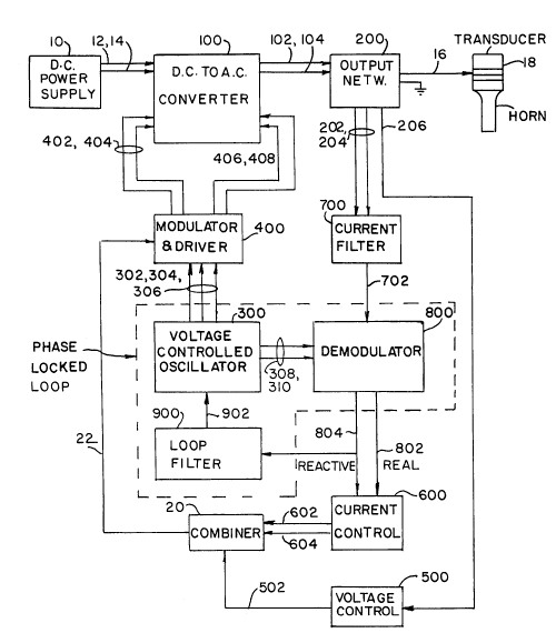
Referring now to the figures and FIGURE 1 in particular, a simplified block
diagram is shown for explaining, in a general manner, the architecture of the new
and improved ultrasonic power supply. A direct current power supply, numeral 10,using conventional means, provides rectified and filtered direct current power via
conductors 12 and 14 to a direct current to alternating current converter unit 100.
The converter unit 100 comprises semiconductor switches for converting the direct
current voltage from the power supply 10 to an ultrasonic frequency, typically 20
kHz, a common frequency used for operating high power ultrasonic welding
apparatus. The switching devices in the converter unit 100 are operated in a switch
mode manner (non-linear) to provide both the frequency generation (20 kHz) and
control of the output voltage using a pulse width modulation technique.
The output network 200 via conductors 102 and 104 receives the ultrasonic
frequency output voltage from the converter unit 100 and provides via conductor 16
the driving voltage and current to the ultrasonic transducer assembly 18. The output
network 200 transforms and matches the output impedance of the converter unit tothe impedance of the transducer assembly. The output network 200 comprises
electrical components forming a resonant circuit in conjunction with the transducer
assembly 18. The output network also provides input signals to certain control
circuits.
-10-
2Q~ 437~
The transducer assembly 18 comprises a stack of piezoelectric discs clamped
between metal masses, and a hom coupled ll ,er~to for coupling the vibrations
produced by the piezoelectric discs, responsive to applied electrical energy, to a
workpiece to be welded. The transducer assembly is of conventional construction
and is well known in the art.
The voltage controlled oscillator 300 is the main frequency and timing generatorfor the entire power supply and its control circuits. It comprises a voltage controlled
oscillator which operates at a harmonic frequency of the fundamental ultrasonic
frequency, 20 kHz in the present embodiment, and a digital frequency divider to
derive system reference signals.
A modulator and driver circuit 400 receives three input signals from the voltagecontrolled oscillator 300, designated by numerals 302, 304 and 306 corresponding to
two times the fundamental frequency (2fp), two times the fundamental frequency
180 degrees phase shifted (2fp), and the fundamental frequency (f p). The
modulator and driver circuit includes linear and digital circuits for generating signals
along conductors 402, 404, 406 and 408 for controlling the operation of the direct
current to alternating current converter 100. A bi-phase signal is generated by the
modulator which provides for the pulse width modulation of the converter unit 100.
The frequency of operation is responsive to the input from the voltage controlled
oscillator 300 and is controlled in time by an analog input signal from the voltage
control circuit 500 and the current control circuit 600. The output signals from the
modulator are amplified by drive stages and then used for controlling the switching
devices of the converter unit 100.
-11-
3 7 ~
The current filter circuit 700 is an electronic filter used for obtaining the
fundamental current signal (f p). An input signal res~l)sive to the operating
current is derived from the output network 200 via conductors 202 and 204. The
input signal contains the fundamental current frequency (f p) and the odd
harmonics of the fundamental frequency. The filter is unique in that it is a bandpass
filter for a range of frequencies around the fundamental frequency, but attenuates
the harmonic frequencies. At the same time, the filter is substantially phase
transparent for the fundamental frequency within the bandpass range, that is,
substantialîy no phase distortion occurs for the signal passing through the filter.
The current demodulator 800 is a synchronous type analog switch or ring
demodulator. The filtered signal from the current filter 700 along conductor 702 is
chopped by digital reference signals from the voltage controlled oscillator 300,conductors 308, 310. The resultant output signals are proportional to the real and
the imaginary components contained in the original current signal. These signalsconvey information as to the value of and the phase relation of the current
components relative to the fundamental frequency drive voltage. The real
component signal is applied as an input signal, conductor 802, to the current control
circuit 600, while the imaginary or reactive component signal, conductor 804, isapplied as input signal to the current control circuit 600 and to a loop filter circuit 900.
2~1~37~
The loop filter 900 is a low pass type filter. The reactive current signal from
conductor 804 is fed to the input of the loop filter. The output signal from the filter,
conductor 902, is used as the phase related control or feedback voltage for the
voltage controlled oscillator 300 for adjusting its frequency. In this manner, a phase
locked loop is created which tends to keep the voltage and current in phase witheach other at the switches of the direct current to altemating current converter 100.
This is accomplished by seeking the frequency for which the reactive current is at a
minimum. Maximum power transfer occurs when minimum stress is applied to the
switching devices of the converter unit 100. The filter is an integral part of the phase
locked loop. Its parameters dictate the overall rate of frequency compensation and
control the stability of the loop.
The cor"binalion of circuits, that is a voltage controlled oscillator 300,
demodulator 800 and loop filter 900, forming what is known as a phase locked loop
(PLL) has been disclosed broadly in the art heretofore, see for instance patent
publication DE 2,726,249, published December 14,1978, assigned to Otto Siebeck
GmbH, or U:S. Patent No. 4,642,581, dated February 10,1987, issued to J. J.
Erickson, entitled "Ultrasonic Transducer Drive Circuit".
The voltage control circuit 500 is used to regulate the overall motional voltagesupplied to the transducer 18. A signal corresponding to the motional voltage isderived in the output network 200. This motional voltage signal is applied to the
voltage control circuit 500 via conductor 206, amplified, and compared with a control
voltage. The result of this comparison is the input signal to the modulator and driver
circuit 400 via combiner 20, conductors 502 and 22. In this manner, the conduction
angle of the switching devices in the converter circuit 100 is controlled for
maintaining a constant motional voltage to the converter.
2Q~37~
During the start cycle, a ramp voltage is generated in the voltage control circuit
500 so as to increase the ou,tput amplitude of the signal to the modulator and driver
unit 400 at a controlled linear rate from zero to a maximum limit dictated by a voltage
control setting for causing the direct current voltage from the converter unit 100 to
increase also from zero to a maximum.
The current control circuit 600 is used for regulating the maximum amount of
current which the power supply delivers during the start and the run cycles. Both the
reactive and the real current components are received as input signals from
conductors 802 and 804, and combined in a manner to protect the power supply in
various modes of operation. The circuit includes a set of differential amplifiers for
limiting respectively the forward current and the reverse current to predetermined
values. The output signals, conductors 602 and 604, also are supplied as a
feedback signal to the modulator and driver circuit 400 via the combiner 20 for
controlling the conduction angle of the switching devices in the converter 100 and,
hence, to control the motional voltage to the transducer. During the start-up cycle,
the circuit may modify the start ramp voltage signal as a function of the transducer
characteristics .
-14-
2~376
Having described now the circuits in broad terms, the following description willmore closely discuss the individual circuits.
FIGURE 2 is a schematic circuit diagram of the direct current to alternating
current converter. It comprises essentially a full wave bridge rectifier and gate
driving networks for controlling the operation of the respective rectifier switches.
The circuit comprises four semiconductor sv.ilching devices 106, 108, 1 10 and 1 12,
each including a power MOSFET device 1 14 for switching the power and a Schottkydiode 116 connected in series with the drain lead for preventing the body diode in
the device 114 from conducting current in the reverse direction. A high speed diode
118 is coupled across the series connection of the MOSFET device 114 and diode
1 16 to conduct reverse current appearing at the swilcl ,ing device.
The switching devices are driven by respective drive stages 120, 122
responsive to the output signals from the modulator and driver circuit 400. The
resulting alternating current output appears at conductors 102 and 104. The
switching circuit essentially is a modulator wherein the output voltage is a function of
the puls~ width modulation. At any time, two switches will be conductive and twoswitches will be non-conductive. A circuit of this configuration termed
"Clamped-Mode Resonant Converter" is described in detail in the article entitled"Constant-Frequency Clamped-Mode Resonant Converters" by F. Tsai et al, IEEE
Transactions on Power Electronics, volume 3, number 4, October 1988, pp.
460-473, figure 2, p. 462.
-15-
201~i~76
-
As seen, the switches are separaled into two half bridge circuits and each half
bridge circuit shares a common gate drive netvJork 120, 122. Each gate drive
network includes circuit components for electrically isolaling each switch and to
provide proper level generation and waveform timing to prevent cross-conduction
during transitions. The waveforms are generated by the modulator and driver circuit
400.
The advantage of this converter circuit resides in the fact that amplitude
changes of the output voltage can be made rapidly without disturbing the phase
relations existing in the phase locked loop which is used to control the frequency of
operation of the converter circuit and, hence, the frequency of the altemating current
output. Also, the circuit enables the resonant load to be driven at a much greater
efficiency. Still further, power can be controlled in both directions, to and from the
load. Finally, energy management is good in that power delivered to the output
network and transducer during an ON period is continuous.
FIGURE 3 is a simplified schematic circuit diagram of the output network.
Since output networks, also known as impedance ",atcl,ing networks, are well
known and have been used heretofore, the circuit will be described only briefly. The
network 200 receives via conductors 102, 104 the alternating current for driving the
transducer 18. The output transformer 208 matches the voltage and current levelsbetween the converter circuit 100 and the transducer assembly 18.
-16-
3 7 i:3
The components in series with the primary v. indil ,9 of the transformer are selected
to cause the primary side together with the secondary side to which the transducer
18 is connected to be electrically resonant at the parallel resonant frequency of the
transducer. A current transformer 210 coupled to the primary side of the networkprovides across resistor 212 a signal commensurate with the current flowing to the
transducer. This signal is both linear and substantially phase transparent with the
current in the primary side and this signal, evident as a voltage across conductors
202 and 204, in turn, is used to control the current supplied to the transducer 18 and
for frequency tuning.
From the secondary winding of transformer 208 an output signal is developed,
conductor 206, which signal is commensurate with the motional voltage driving the
transducer 18, i.e. the voltage proportional to the amplitude of vibration. Thisvoltage is fed to the voltage control circuit 500 and used, in turn, for regulating the
motional output amplitude of the transducer 18.
FIGURE 4 is a simplified schematic circuit diagram of the current filter 700. The
filter is an electrical bandpass filter which will attentuate frequencies falling outside
the band frequencies, but which will pass signals within the selected frequency
band. One special feature of the filter resides in the characteristic that for the
frequency range within the pass band, the phase shift of a signal from input to output
will be minimal, i.e. the filter is phase transparent.
~01~37~
-
The pulsating output voltage from the direct current to alternating current
converter is naturally filtered by the output network 200 and transducer 18. Theoutput signal contains various frequency components, namely the fundamental
frequency (20 kHz) and odd harmonics of the fundamental frequency. This gives
rise to similar and related current signals. Of prime interest is the fundamental
frequency current signal. At resonance, the fundamental frequency current and
voltage will be in phase with one another. Hence, the first object of the filter is to
pass the fundamental frequency current signal but to attenuate the harmonic signals.
The current signal commensurate with the current flow between the network
200 and transducer 18 is supplied via conductors 202, 204 to the current filter circuit
700. The circuit, see FIGURE 4, comprises two stagger tuned parallel resonant
circuits. The operating frequency and Q (quality factor) of each tank circuit 704, 706
is selected to have equal and opposite phase slope within the frequency band of
interest. For instance, for a fundamental frequency of 20 kHz, tank circuit 704 may
be tuned for 19 kHz and circuit 706 for 21 kHz, providing a pass range and phasetransparency for the fundmental frequency of 20 kHz. The signals from the tank
circuits are then summed in a summing circuit 708 to provide an output signal along
conductor 702 containing only information with regard to the fundamental frequency
as harmonic frequencies above or below the selected band width were attenuated
by the resonant tank circuits. The signal along conductor 702, therefore, represents
a signal corresponding to the amplitude and phase of the fundamental frequency of
the current flowing between the converter 100 and the transducer 18.
-18-
20 ~ 437~
FIGURE 5 is a schematic circuit diagram of the demodulator 800. In order to
maintain the transducer 18 at its resonant operating point, the current and voltage
output from the converter 100 must be in phase. The current signal, filtered in circuit
700, is applied via conductor 702 to the demodulator 800 to obtain both the
magnitude and phase information of the input signal.
The demodulator comprises a set of synchronous type analog switches. The
analog output signal 702 from the filter 700 is applied to both analog switches 806
and 808, which are commercially available integrated circuit devices. Switch 806also receives a digital signal f'p via conductor 308 commensurate with the
fundamental operating frequency, but phase shifted by ninety degrees. Similarly,switch 808 receives a digital signal f p via conductor 310 commensurate with thefundamental operating frequency, but without phase shift. Therefore, the signal
provided by conductor 804 will represent the imaginary or reactive current
component flowing to the transducer 18, while the signal provided by conductor 802
will be commensurate with the real component value of such current. With no
imaginary current component present in the current flowing to the transducer 18, the
output signal of conductor 804 will be zero. If an imaginary component is present,
the output signal along conductor 804 will be a plus or a minus voltage signal.
-19-
20~376
FIGURE 6 is a schematic electrical circuit diagram of the loop filter. The filter
essentially is a low pass filter and is used to process the imaginary current
component signal from the demodulator 800. The harmonic frequency content is
blocked and an average direct current error voltage is obtained and sent as a
correction (control) signal to the voltage controlled oscillator input for adjusting the
frequency of the oscillator. The filter comprises an integrating circuit 904 which
receives the output signal, via conductor 804, from the demodulator as describedabove.
The integrator 904 has controlled time constants which govern the overall
response of the phase locked loop and which are selected for stability and rate
considerations. A phase and current shift will cause the integrating circuit capacitor
906 to charge or discharge. The resultant voltage will cause the voltage controlled
oscillator frequency to change in a manner to cause a reduction in phase shift. The
voltage at the integrator output, conductor 902, will settle and become stable when
the phase shift approaches zero (tuned condition). Changes in phase shift will
cause a change in output signal which is fed to the oscillator to cause a
corresponding frequency correction. The output voltage from the loop filter,
therefore, is a voltage signal representative of the phase relation between the
current and the voltage applied to the transducer 18 and such voltage signal will be
a constant direct current voltage when a substantially zero phase shift condition
prevails, that is, the voltage controlled oscillator provides the proper frequenGy for
precise parallel resonant operation of the transducer.
-20-
~Q s 437S
-
FIGURE 7 is a schematic electrical circuit diagram of the voltage controlled
oscill~tor. A specific circuit is shown, but other arrangements could be used for
providing the same function. The oscillator includes a commercial oscil~?tory timer
circuit 312, such as Texas Instruments No. 555, arranged to operate in an astable
mode. The components 314, 316, 318 and 320 are selected to cause the oscillator
to operate at a frequency of four times the parallel resonant frequency 4fp of the
transducer. The frequency of operation of the timer 312 is also a function of the
value of the direct current voltage signal supplied to its input control by conductor
902, the signal from the loop filter. Resistors 322, 324, 326 and 328 form a voltage
shifting and scaling network which couples the control or feedback voltage input to
the control signal pin on timer 312. As the voltage at the input pin of timer 312 is
made more positive, the frequency of the timer decreases and, conversely, a morenegative control voltage will cause the frequency to increase.
Variable resistor 326 is used to set the amount of frequency deviation which thecontrol voltage will effect. In this manner, a limit is set for the range of frequencies
(bandwidth) within which the power supply will operate. Variable resistor 314 isused to adjust the center frequency.
The output from the voltage controlled oscillator 312, operating at four times the
fundamental frequency, is sent to a D-type flip/flop 330 connected to form a divide
by two circuit. The frequency signal 4fp from the oscillator is thus divided by a
factor of two to yield two signals, namely 2fp conductor 302, and its
complementary,180 degrees shifted, signal 2fp, conductor 304.
~01~76
Two aJdilional D-type flip/flop circuits 332 and 334 are used to generate
r~ference signals. Flip/flop 332 again is connected as a divide by two circuit, the
signal 2fp being co,1nected to its input. The outputs from this flip/flop 332 are the
fundamental frequency signal fp apparent at conductor 306 and conductor 310
and the complementary signal fp. These latter signals are 180 degrees out of
phase with one another. The signal 2fp acts as a clocking signal for the flip/flop
334 and the signal f p acts as the data input. The result is that flip/flop 334
produces an output signal f'p conductor 308, which signal is the fundamental
frequency, but shifted by ninety degrees. The signals in digital form along
conductors 308 and 310 are coupled to the demodulator 800 as previously
described, whereas the signals of conductors 302, 304 and 306 are coupled to themodulator and driver circuit 400.
The voltage (amplitude) control circuit is shown in FIGURE 8. A parameter of
prime importance to an application of this type of ultrasonic apparatus is the
amplitude of mechanical vibration provided by the transducer and hom. As
described above, a motional amplitude responsive signal, conductor 206, FIGURE
3, is derived in the output network, which signal is proportional to the driving voltage
applied to the transducer. This voltage is known also as "motional voltage". Themotional voltage is scaled and rectified. It is then summed with a reference voltage
to produce an error signal. The error signal is amplified and fed to a combiner and
to the modulator and driver circuit input. This feedback loop has the purpose ofmaintaining a desired motional amplitude setting. Because the motional voltage is
sensed, the circuit arrangement is such as to maintain a set amplitude irrespective
of line voltage variations and of loading effects reflected on the power supply.
_ 2~437 :3
Provisions are made to vary the reference voltage either intemal or extemal to
the power supply. In this manner, the amplitude of vibralioil may be set by a control
potenlio",eter or by an exle,~al signal, such as a process derived signal. The
system has a fast response time so that an amplitude variation can be effected even
during a particular weld cycle. During the start-up period, the reference voltage
signal is modified by a ramp function generator. The result is that the motionalvoltage and the resultant amplitude of vibration starts from a rest condition and
increases at a set linear rate until the preset point of regulation is reached.
Therefore, the transducer is caused to increase its amplitude of vibration in anorderly manner at a linear rate, rather than in a stepwise fashion.
The motional voltage signal, conductor 206, is rectified by rectifier 504 and
filtered by capacitor 506. The resultant direct current signal is sent to an integrating
amplifier 508. At the amplifier 508, the direct current signal responsive to the driving
voltage applied to the transducer 18 is compared with a reference voltage setting.
The reference voltage value may be a set point signal from an amplitude adjusting
potentiometer 518, or a variable signal, such as a ramp signal originating at the
ramp voltage generator 510 comprising an amplifier 512 and capacitor 514 in
conjunction with a voltage source and series connected switch 516 having a "STOP"
position and a "RUN" position.
2Ç~14~7~i
-
If the amplitude responsive signal is lower than the reference voltage, the output
signal from the amplifier 508 will increase the signal level to the CO~lt ner 20 and to
the modulator and driver circuit 400 for causing the output voltage provided by the
converter to increase. If the amplitude responsive signal is greater than the
reference voltage, the output from the amplifier 508 will decrease and cause themotional voltage applied to the transducer to decrease.
For starting the power supply from rest, the ramp generator 510 is used to
modify the reference voltage from potentiometer 518. At rest, switch 516 is in the
"STOPr setting as shown. The ramp generator clamps the reference voltage to a
zero value. When the switch is moved to the ~RUN' position, the ramp generator
output slowly rises at a linear rate and allows the reference voltage to rise also. This
occurs until the clamp diode 520 is no longer conductive, at which condition thepower supply is running at a steady state condition. It will be understood, of course,
that the switch 516 will be an electronic switch.
-24-
20~437~
FIGURE 9 is a circuit diagram of the current control circuit 600. The current
control circuit components regulate and limit the normal output current levels
produced by the power supply. During a normal sequence of power supply
operation, there exist various conditions in which these circuit components comeinto operation.
During the operate or run time, the power supply may be required to deliver
more power than it can safely provide. The operating current level is sensed at the
output network 200, processed by the current filter 700 and by the real current
component circuit of the demodulator 800. The resultant signal is compared in the
current control circuit 600 with a reference signal defining maximum current. Any
resulting difference or error signal corresponding to excessive current is used to
control the modulator and driver circuit 400 after having passed through the
combiner 20. The action is to reduce the alternating current voltage amplitude
output from the converter 100 and, hence reduce and adjust the current to its preset
maximum value. This control is linear in its characteristic.
-25-
201~3~6
-
The transducer 18, moreover, is a mechanically resonant device and will store
energy. The device is bidirectional in that it will both use and generate energy, that
is electrical current. In order to control the amplitude of vibration of the transducer at
a fast rate, the power supply must be able to receive as well as generate a
maximum current. The output from the real current component portion of the
demodulator, conductor 802, will change its polarity and level corresponding to the
amount of current and its direction to or from the transducer. The output from the
current control circuit will control, via the combiner 20, the modulator and driver
circuit 400 to either decrease or increase the effective alternating current voltage
output from the converter 100 depending upon the direction of current flow to or from
the transducer.
During the start-up cycle, large reactive current components may be present in
the current path from the converter to the transducer. In this event, a sample of the
imaginary or reactive component signal from the demodulator, conductor 804, is
combined with the real component current signal. The result is a load line shaping
or modification of the current level set point to better protect the switching devices
from failure caused by excessive energy switching during periods of load transitions.
-26-
2~376
-
Also, during start-up, large mechanical homs may require excessive energy to
reach a set amplitude of vibration. In this case, if the current requirements are too
great for causing the transducer with horn to reach its set amplitude during an
allotted time interval, the current control circuit will modify the start cycle time by
automatically reducing the signal to the modulator and driver circuit 400. This
feature will lengthen the start up time and keep the power supply from reaching an
overload condition.
The real component of the current signal, conductor 802, from the demodulator
800 will have a value dependent on the current flow direction. Its polarity will be
positive if the current flow is toward the transducer 18 and will be negative if the
current flow is in the direction from the transducer. This real current component
signal is sent to two integrating amplifiers 605 and 606 together with a respective
reference signal. A signal corresponding to the maximum permissible forward
current is generated by potentiometer 608 and the signal corresponding to the
maximum permissible reverse current is generated by potentiometer 610.
If the actual forward current signal exceeds the reference forward signal value,the amplifier 605 will produce an output voltage signal to the combiner 20 and to the
modulator and driver circuit, conductor 602, to decrease the output of the powersupply by reducing the alternating current voltage from the converter. This condition
will either limit the rate of rise of the current to the transducer or reduce the current
to a predetermined safe level.
-27-
._ 201~37~
If, however, the reverse current signal exceeds the reference reverse signal value,
the amplifier 606 will produce an output voltage signal to the modulator, conductor 604, for
causing an increase of current flow from the power supply, i.e. raising the altemating
current voltage from the converter. This action will limit the rate of decrease of current flow
from the transducer 18 to a safe level.
A portion of the imaginary or reactive current component received from the
demodulator via conductor 804 is summed together with the real current component at
junction 612. This summing action results in that the total amount of forward current
during start up of the power supply is controlled if a mistuned condition prevails.
FIGURE 10 depicts the combiner circuit which combines, at junction 24, the output
signal from the voltage control circuit 502, the voltage control signal, with output signals
from the current control circuit provided either by conductor 602 or conductor 604 to
produce via buffer amplifier 26 a combined control signal at conductor 22 to the modulator
and driver circuit 400. This control signal serves as a composite control signal to regulate
the output voltage provided by the converter 100. If the transducer operates within
predetermined levels of current flow, only the amplitude control signal 502 will be effective
as output from the combiner 22. If the current flow to the transducer or from the
transducer is above the desired level, the voltage control signal is modified by the current
responsive signal as described.
-28-
' 20~37S
FIGURE 11 is a schematic circuit diagram of the modulator and driver circuit
which receives the frequency responsive signals from the voltage controlled
oscillator and the combined voltage control signal from the voltage control circuit and
the current control circuit. Therefore, the modulator and driver circuit 400 operates
on a voltage control signal and the signals generated by the voltage controlled
oscillator providing output signals for suitably controlling the operation of the direct
current to alternating current converter 100.
The timing signal from the conductor 302 (double frequency signal 2f p)
coming from the voltage controlled oscillator 300 is sent to an integrating amplifier
circuit 410 which causes a triangular shaped output signal with equal slopes. This
signal, in turn, is applied to a comparator circuit 412. The comparator circuit 412
also receives, via conductor 22, the steady state composite signal from the comb ner
22, representing a voltage control signal. The comparator is used to compare thecontrol voltage with the triangularly shaped signal. The output from the comparator
412isfedtoaNANDgate414andanANDgage416. TheNANDgate414also
receives the timing signal 2f p from conductor 302. The AND gate 416 receives
as its second input signal the signal from conductor 304 representing the signal of
double frequency of the imaginary current component 2f p. The output from the
NAND gate 414 and the output from the AND gate 416 are applied as inputs to a
respective flip/flop circuit 418 and 420, each of which receives also a signal fp
from conductor 306, representing a timing signal.
-29-
376
The output signals from flip/flop 418 and flip/flop 420 exhibit a variable phaserelationship with each other, varying from a minimum of zero degrees, which will be
minimum output voltage from the converter 100, to a maximum of 180 degrees,
providing maximum output voltage. The buffer amplifiers 422 form driving stages.The respective 180 degrees shifted output signals appearing across conductors 402
and 404, and conductors 406 and 408 are coupled to the driving stage transformers
120 and 122 of the converter circuit, see FIGURE 2. There~or~, the converter 100 is
caused to provide by pulse modulation a feedback controlled altemating current
output voltage, accurately controlled in respect to frequency, amplitude of motional
voltage and maximum current flow. Hence, the power supply has all the desired
attributes set forth at the beginning of the specification.
While there has been described and illusl~ate(l a preferred embodiment of the
invention, it will be apparent to those skilled in the art that various changes and
modifications may be made therein without departing from the broad principle of this
invention, which shall be limited only by the scope of the appended claims.
What is claimed is:
-30-