Note: Descriptions are shown in the official language in which they were submitted.
201~480
- 1 -
AN OPTICAL INTERCOMNECT AR~NGEMENT
- Backgrourld of the Invention
This invention relates to electrooptic waveguide circuits and, more
particularly, to methods and apparatus eor coupling energy between electrooptic
waveguide substrates.
Research on integrated optics has been going on for some years
now, with particular emphasis on developing effective and efficient electroopticwaveguide switches/modulators. Such devices are very attractive for signal
encoding, multiplexing, optical frequency shifting, signaling and, particularly, 10 switching. There is a large volume of literature on the subject of electrooptic
waveguide modulation. The following two references, which present tutorial
reviews, form a good starting point. Waveguide Electrooptic Modulators, Rod C.
Alferness, E:EE Transactions on Mierowave ~heory and 'lechni~lues, Vol. MTT-30, No. 8,
August 1982, pp. 1121-1137; and Guided-Wave Devices for Optical
Communication, Rod C. Alferness IEEE Joumal of Quannml Electronics, Vol. QE-17~
No. 6, June 1981, pp. 946-959. A further discussion of these articles will be made
hereinbelow with reEerence to the drawings.
,, Implementing one switch, or even realizing a number of switches on
'l a single substrate is only of marginal value. The key to utilization oE the
technology must lie in the ability to easily and effectively construct relatively large
switching networks. To achieve that, three issues must be addressed. The first
issue is the ability to create many switches on a single substrate. The second issue
is the creation of an efficient architecture for building an optical switch network
from individual switches and/or from smaller switch networks. The third issue isthe development of means for interconnecting the substrates that contain the
switches and the switch networks. ~-
The lattèr two issues need better solutions than the ones that are U
available in the prior art.
Transmission of information from one electronic circuit board to
another via an optical medium has been accomplished with fibers. This is often
referred to as the optical backplane approach. Generally, this approach involves
':
:. ,: ~:
*
.. .
' :.
2~54~0
- 2 -
the use of light emitters and light detectors at the transmitting and the receiving
ends of the transmission medium. It is an inefficient approach for interconnecting
boards or substrates of electrooptic waveguides that contain a modest amount of
logic (e.g., switches) per connection.
In the optical computing field, 3D interconnections are implemented
with fiber arrays (e.g., U.S. Patent No. 3,872,293 issued to E.L. Breen on March1~, 1975), or in "free space". In "free space", the connection pattern is fixed since
the optical signal paths are controlled in bulk by the medium. That, per se, is not
an insurmountable impediment. It is known to perform a perfect shufEle on an
incoming set of signals. The perfect shuffle permits an arbitrary interconnection to
be realized by the use of a sufficient number of interconnection stages.
Alas, the connection techniques that are used in free space optical
computing are not applicable to waveguide electrooptics because these techniquesbasically rely on emission of light by the sending elements and detection of light by
is the receiving element. In a sense, this is the same technique that is used in the
optical backplane. No specific match in polarization is generally necessary Eor the
detection function.
Interconnection in three dimensional space has also been employed
in the electronics arts (in contrast to optics), although in a different manner. For
example, in "Compact Layout of Banyan~FFT Networks" Proc. CMU Con.~ VLSI syst.
Computations, 1982, pp. 186-195, D.S. Wise described an arrangernent whereby a
crossover network can be decomposed in a manner that permits realization of the ~ -
overall circuit from a collection of circuit boards that are stacked and
interconnected in three dimensions. Of course, the spatial arrangement describedby Wise is useful only for the particular class of networks that he described; but
once he decided that such a spatial organi~ation is useful, no major impedimentswere presented for implernenting the desired electrical interconnection. Electronic
circuit wi}e connections for the described arrangement are quite conventional. -~
That is not the case with integrated optics where light travels in
controlled channels as described above. The polarization state of the light is very -
critical and the positioning alignment of the elements that emit light and the
elements that accept the light is exacting. ~ ~;
.. '".~, `` .
r ~ ~ ,
201~80
- 3 -
Summarv of the Invention
~- In accordance with the principles of our invention, an optical
crossbar switch is reali~ed by joining substrates, or plates, of electrooptic
modulators, essentially through butt coupling of the plates. More speci~lcally, a
S crossbar switch is realized by stacking a plurality of fan-out or splitter plates,
stacking a plurality of fan-in or combiner plates, rotating one of the stacks with
respect to the other stack, and joining the rotated and the unrotated stacks.
Each splitter plate accepts an injected optical signal and, under
voltage control electrooptic modulations on the plate, routes the injected signal to
one of M splitter outputs.
Each combiner plate accepts injected optical signal at each of N
combiner inputs and, under voltage control of electrooptic modulators on the plate,
routes a related input to the output of the plate. By stacking N splitter plates and
M combiner plates, and rotating one of the stacks, the arrangement yields the
capability to route any injected input on any splitter plate to any selected combiner
plate and to route the signal received at the input of the combiner plate to theplate's output.
The different light polarizations that are required for the two plate
stacks are obtained in our invention with different means. One such means is a
bireEringent half wave plate interposed between the splitter stack and the combiner
stack. The plate provides a rotation of 90 degrees in the spatial orientation of the
polarization plane of light. Another means is manufacturing the combiner plates
from a material that is compatible with the polarization plane orientation of the
3 light injected into the splitter plates and into the combiner substrates. For
example, for the important Lithium Niobate material system, when the splitter
. plates are manuEactured from an x-cut crystal, the combiner plates are
manufactured from a z-cut crystal. Still another means is including light
polarization converters at the outputs of the splitter plates, at the inputs of the
combiner plates, or both.
In accordance with one aspect of the invention there is provided an
arrangement comprising: an M plurality of output plates each having N output
3 ports delivering optical encrgy substantially along a line, said output plates being
substantially parallel to each other, thereby forming an array of output energy
'
`..~.~i~'
201~80
. ports; an N plurality oE input plates, each having M input ports for receiving optical
energy substantially along a line, said input plates being substantially parallel to
each other; and means for coupling the optical energy of output j of plate i in said
M plurality of output plates to input i of input plate j in said N plurality of input
S pla~es, where i is an integer in the range 1 to M and j is an integcr in the range 1
to N.
`1 A more in-depth understanding of our invention can be had by
perusing through the detailed describing and the drawings wherein:
Brief Dessription of the Drawin~
FIG. 1 illustrates the general structure of an electrooptic
switch/modulator;
FIG. 2 presents a block diagram of a waveguisle electrooptic routing
switch using fan-out/fan-in principles;
FIG. 3 depicts the layout of modulators on a plate that routes on
applied optical signal to one of eight outputs;
1 FIG. 4 shows the stacking and interconnection of input coupler
plates and output coupler plates to form an 8x8 crossbar switching network;
FIG. S presents a solution to a signal polarization problem in the
FIG. 4 arrangement, using a half wave plate;
FIG. 6 shows the use of focusing lens with the arrangement of FIG.
S;
FlG. 7 presents a solution using different cut crystals for the
combiner plates and the splitter plates;
FIG. 8 illustrates the structure of a polarization converter;
FIG. 9 depicts interconnections of combiner plates and splitter
plates that contain a polarization converter; and
FIG. 10 illustrates an embodiment where the spatial orientation of
the combiner plates is other than 90 with respect to the splitter plates.
A brief description of relevant portions of these articles is presented
herein in conjunction with FIG. 1 for the sake of completeness.
:~:
- ~.
:~
20~5~80
Integrated waveguide modulators of a form not unlike the one
shown in FIG. 1 can be created in various materials and accordance with various
techniques. A waveguide modulator can be realized, for example, with light
channels created in a Lithium Niobate substrate, such as channels 10 and 15 in
FIG. 1. The channels may be created by diffusing Ti into the substrate, thereby
causing the refractive index in the channels to be greater than in the surrounding
region. When the difference in refractive indices is large enough, light that isinjected into channel 10 at point 11 travels through the channel without dispersion
into region 20. Somewhere along its path, the light traveling in channels 10 and 15
passes through region 30 of the substrate. Within region 30, channels 10 and 15
are situated in close physical proximity to each other and are bordered by
electrodes ~1 and 42. By choosing an appropriate separation between the
waveguides and the interaction length, all of the light incident on one of the
waveguides exits in the other via distributed evanescent coupling. Thus, the light
traveling through channel 10 exits the substrate at point 17. In a similar fashion,
light may be injected into channel 15 at point 16. It exits at point 12. Applying a
voltage to the electrodes causes a phase shift in the light traveling through channel
10 within region 30. The phase shift reduces the coherent coupling between
waveguides 10 and 15. With an appropriate voltage the output optical signal at
port 17 reduces essentially to zero. The same conditions apply to light injectedinto channel 15.
The arrangement depicted in FIG. 1 is akin in its operation to a
cross-connected double-pole double-throw switch. When no voltage is applied to
electrodes 41 and 42, light injected into ports 11 and 16 exits at ports 17 and 12,
respectively. This is the "pass thru" connection. When no voltage is applied, the
light of channels 10 and 15 crosses over to the other channels and exits at ports 16
and 12, respectively. This is the "crossover" connection. Viewed another way,
when a detector is placed at one of the outputs and different signals are applied at
the two input ports, then the FIG. 1 circuit serves as a selector, combiner, or
multiplexer. Conversely, when a detector is placed at both outputs, and only oneinput has an applied input signal, then ~he FIG. 1 circuit serves as a demultiplexer.
Thus, the modulator of FIG. 1 can be a switch, a multiplexer, or a demultiplexer.
20~480
- Sa -
Waveguide electroop~ics switches, or couplers, can be used as cross-
coupled double-pole, double-throw switches, as described above. The need,
however, is to create a larger and more robust switch architecture. FIG. 2
presents one fulfilment of this need.
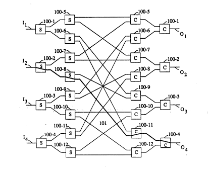
S FIG. ~ includes 24 electrooptic couplers, with 12 arranged as
dynamically controlled splitters and 12 arranged as combiners. Four primary inputs
Ii ~i=1,2,3,4) are connected to four first level splitters 100-1, 100-2, 100-3, 100-4,
and the two outputs of each of the first level splitters are each connected to asecond level of splitters 100-S through 100-12. The second level of splitters results
in sixteen outputs. The sixteen outputs of the second level of splitters are
connected to sixteen inputs of eight second level combiners 110-S through 110-12.
` The outputs of the eight second level combiners are connected to four first level
~, combiners that yield four primary outputs O, (i= 1,2,3,4). If one were to number
the sixteen outputs and the sixteen inputs in a manner that corresponds to the
numbering of the inputs and the outputs, the interconnection of the outputs to the
inputs in FIG. 2 can be defined by "output i is connected to input (i+4) mod 15".
Generalizing on FIG. 2, it can be said that the figure depicts a
routing switch arrangement having M=2m inputs and ~=2" outputs. Each input is
applied to a splitter that, through n successive binary fan-out stages, allows the
input to be connected to any one of N outputs. Each output in the set of N
splitter outputs that are developed for each input is connected to an input o~ adifferent one of N combiners. Each combiner has M inputs and m combining
binary fan-in stages that develop a single output. The values of M and N need not
be the same and they need not be binary.
To accomplish switching with the FIG. 2 arrangement, it is necessary
to switch actively only the splitters or the combiners. For example, each of thecombiners can be arranged to simply add the two inputs, and since only one~o~ the
'~ inputs would receive information, no switching is necessary in the combiner. On
,~ the other hand, by making both the splitters and the combiners active, insertion
loss and crosstalk can be minimized. When reducing the crosstalk and insertion
loss is important, such switching is the preferred approach. Thus, to switch a signal
from I~
2(~5
- 6 -
to 04, for example, path 101 must be enabled. That requires that couplers 100-2 and
100-9 should direct their received light downward, coupler 110-11 should select itS
lower input signal, and coupler 110-4 should select its upper input signal.
An (NxN) switch of the type described above requires a total of 2N(N-
S 1) couplers. This is almost double the number of switches that are required in aconventional (NxN) crossbar switch. However, the FIG. 2 architecture has a number
of important advantages. For example, the interconnections of the splitter couplers
and of the combiner couplers, among themselves, contain no crossovers. In
waveguide electroopdc technology, this is a clear advantage.
Although FM. 2 presents a useful architecture, it does leave the question
of how to create the splitter couplers and the combiner couplers, and how to connect
the splitter couplers to the combiner couplers.
As for the manufacture of the combiner and splitter couplers, in
accordance with the principles of our invention, the splitter couplers and the
15 combiner couplers are divided into sets, and the sets are manufactured as integral
units. A splitter coupler set is the collection of couplers to which a particular input
port of the FIG. 2 arrangement can send a signal. Similarly in connection with
combiner coupler sets. In the case of input I1, for example, the set includes splitter
couplers 100-1,100-5,and 100-6. Inaccordancewiththeprinciplesofour
20 invention, therefore, an entire coupler set is manufactured on a single plate.
FM. 3 illustrates the layout of a plate that routes one optical input to one
of eight outputs and thereby encompasses an entire combiner coupler. In operation,
an optical signal is injected in entry port 31. The signal enters the first level switch
(32) which directs the signal to either one of two outputs. We call this switch "a
25 splitter" because diagrammatically it looks like it splits the incoming path into two
outgoing paths. Each outgoing path of the first level splitter is connected to a second
level splitter. There are two second level splitters (33,34) and they produce four
outgoing paths. The second level output paths are connected to third level splitters.
The four third level splitters (35-38) have eight output paths.
The signal entering port 31 is injected into either splitter 33 or
splitter 34; and the splitter with the signal routes it to either one of its ontputs. Since
the state of the splitter without the signal is completely irrelevant, the second level
splitters share a common control signal. Similarly, the third level splitters share a
comrnon control signal. The optical signal of port 31 is routed in this manner to one
35 of the eight output paths.
~59~8~
- 7 -
Thus, with n splitter levels (n=3) and n control signals (n-3) the FIG. 3
plates routes the injected signal to one of 2n (2n=8) paths. The control pads that
control the routing, and the signals that are applied to the control pads are not shown
`~ in FIG. 3 for sake of simplicity. It is understood, however, that an actual
S implementation includes the necessary controls. Since the combiner couplers
arrangement is completely symmetric tO the splitter couplers arrangement, in
accordance with our invention the entire switch can be made up of identical plates.
Simply reversing the entry point of light converts an combiner coupler into a splitter
coupler.
As for the interconnection of the combiner couplers to the splitter
couplers, FIG. 4 depicts our novel arrangement for the plates of FIG. 3, which
realizes the switch architecture of FIG. 2 -- an 8x8 optical crossbar switch. InFIG. 4, the plates of the splitter couplers are stacked substantially parallei to each
other with the edges that contain the eight outputs being lined up with each other.
15 The result of such stacking is that a rectangular array of output ports is formed when
viewed at end-on. The rows of the array are formed from the collection of output¦ ports of each horizontal plate, and the columns of the array are formed from the
collection of output ports having the same relative position in each of the horizontal
plates. For a proper ali~nment, of course, the spacing between the combiner plates
20 must be adjusted to correspond to the spacing between the output ports of the splitter
plates, and vice-versa~ `
The arrangement of plates as shown in FIG. 4, once invented for the ~ ;
purpose of realizing the interconnection pattern of FIG. 2, presents no
implementation problem in the electronic arts. Just as Wise interconnected his
25 circuit boards to fo~n a Banyan Network, so would the FIG. 4 interconnection of
plates be realized. In the integrated waveguide electroopdc art, however, the
¦ interconnecdon is not simple because the polarizadon of light exiting the splitter
plates must be tnatched, in most waveguide material technologies, to the required
polarization of light that enters the combiner plates to rninimize the voltages
30 required to control the switches.
FIG. 5 presents one soludon in conformance with the principles of our
invention. In FIG. 5, the splitters and combiners of the FIG. 4 arrangement are
identical and, therefore, the crystal cut of the plates requires a particular polarization
mode of the light passing through the channels. Because of the different spatial35 orientation of the combiner and splitter couplers, a rotation in the polarization plane
t ot the light is necessary. To achieve this rotation, rhe combiner and spliner couplers
ii ,
~'
: æ~
- 8-
are separated somewhat from each other, and a half wave plate 150 is inserted
therebetween. The polarization axis of plate 150 must be adjusted properly (at 45
with respect to the plane of the plates) and when so adjusted, the polarizatdon of light
exiting the splitter couplers is rotated by 90 prior to its injection into the combiner
S couplers. Imaging lenses can be included on either or both sides of plate 150 for
more effective focusing of the light onto the combiner channels. That is, when it is
deemed that the coupling loss between the splitter plates and the combiner plates is
too great because of the spacing introduced by plate 150, one can separate the two
stacks stdll further by two focal lengths of a focusing lens and insert two such lens as
10 shown in FIG. 6. FIG. 6 is the front view of the stack arrangement. It should be
realized, of course, that the use of half wave plate 150 requires the orientation of the
combiner plates to be close to 90 away from the orientation of the splitter plates. If
one wishes to employ a magnetic means for polarization rotation, a Faraday rotator
, can be substituted for plate 150; and with such a rotator the 90 spatial orientation
15 would not necessarily have to be maintained.
In accordance with another aspect of our invention, the FIG. 2 structure
is created with butt coupling of the combiner and splitter couplers, as depicted in
FIG. 7.
Unlike the FIG. 5 realizadon, the combiner couplers and the splitter
20 couplers of the FIG. 6 realization are not identical. Specifically, the combiner
couplers and the splitter couplers are manufactured for different preferred light
polarizadons and, more specifically, for preferred light polarizations that are 90
rotated. The splitter plates can be manufactured, for example, for a preferred light
polarization (e.g., requiring minimum control voltage) that is perpendicular to the
25 large flat surface of the plates. The plane of polariza~ion of the incorning signal is
then arranged to be perpendicular to the large surface of the splitter plates. The
polarization of light exiting ~he splitter couplers and entering the combiner couplers
is consequently in a plane that is parallel to the large surface of the combiner plates.
.1 ~ For light to be accepted by the combiner couplers, that requires the combiner plates
, 30 of FIG. 6 to be manufactured from a matçrial with similar polarization mode
preference.
The different combiner and splitter plates can be created from different
~;~ materials, or from the same material. For example, in our preferred embodiment
Lithium Niobate substrates are used. One of the plates (e.g. the combiner plates) is
35 manufactured with an x-cut crystal orientation, while the other is manufactured with
a z-cut crystal orientation.
., .
~; .
4~
. - :
In accordance with still another aspect of our invention, butt coupling of
the plates is achieved nevertheless with the same material and the same crystal cut of
the material. In I J.S. Patent 4,384,760 issuecl on May 24, 1983, R. C. Alferness
discloses a novel electro-optic device that can controllably alter the polarization of
5 light that passes through the device. This device is also described by Alferness and
Buhl in "Waveguide electro-optic polarization transforrner", Appl. Phys. Lett. 38(9),
May 1, lg81, pp 655-657. FIG. 8 is essentially a copy of PIG. 2 in the
aforementioned patent. Briefly, the device described in FIG. 7 includes a light
channel 25, electrodes 22 and 22 which provide an input phase shift to the light10 within channel 25, electrodes 24 and 24 which provide mode conversion, and
electrodes 23 and 23 which provide an output phase shift. The input phase shift
electrodes change an injected light that is circularly or ellipdcally polarized into an ~ ~ -
linearly polarized light. The mode converter electrodes convert the polarized light
from one mode to another, and the output phase shift electrodes insure that the light
15 exiting the device is, again, linearly polarized.
FIG. 9 presents the front view of a plate that includes a polarization
converter at each output. With this converter, butt coupling of the plates as in FIG. 7
is accomplished with identically manufactured plates and without the need of a
separate polarization conversion means. It may be noted that the spatial phase shift
20 induced by the polarizadon converters in both the combiner plates and the splitter
plates is only 45. Of course, if one is willing to have combiner couplers that are not
identical to the splitter couplers, then one can insert polarizadon converters in only
one of the coupler ~ypes, and those converters would need to provide a 90 spatial
phase shift. Such polarization converters would not need to include the input phase
25 shift electrodes because, in the application of FIG. 9, the input signal is of a known
polarization.
The arrangement of FrG. 5 illustrates the condition where the combiner
plates and the splitter plates are at 90 to each other. That is neither a requirement
nor a limitation of our structure. The only requirement is that the light at the output
30 ports of the combiner plates, or splitter plates, should be efficiently coupled (i.e.,
with minimum loss) to the input ports of the splitter plates, or combiner plates.
Since the channels of the combiner plates are situated directly across from the
channels of the splitter plates, one can visualize the centers of the two sets of
channels to be connected by pins about which the plates can rotate. With no spacers
35 between plates, the structure is unstable, and can be collapsed so that the plates of
each set (combiners and splitters) are touching each other. This is shown in FIG. 10,
2~S~
,
diagrams A and B. Of course, the B structure is a more compact and physically :
stable implementation, but it requires a rotation of the polarization of light through
less than 90(oc). That can be accomplished with the plates used in the embodiment
. of FIG. 9, but with the input phase shift electrodes included and the voltage on the
S phase shift electrodes adjusted to provide the desired spatial phase shift.
--
'
:~:
. '' .
. ,,~ ,".
;' '~'''