Note: Descriptions are shown in the official language in which they were submitted.
CA 02017~79 1998-02-04
COMMUNICATION CIRCUIT FAULT DETECTOR
BACKGROUND OF THE INVENTION
This invention relates to a communication circuit fault detector for testing a
communication circuit.
The term communication circuit refers generally to a circuit that receives an
input data signal at one location and reproduces a substantially identical output data
signal at another location. Communication circuits are ubiquitous in data processing
systems, being used for communication between separate data processing equipment,
between separate printed circuit boards in the same data processing equipment, and
between separate components on the same printed circuit board.
The usual method of testing a communication circuit is to perform a loop test
by sending known test signals through the communication circuit, looping the test
signals back to their point of origin, and comparing the returned test signals with the
original test signals. Prior-art apparatus for this purpose comprises devices for
generating and comparing the test signals, and a switch that connects the output side
of the communication circuit to either its normal output line or a loop-back line.
During data communication, the switch is set to the normal output line position. To
test the communication circuit, normal data
FB923
2017~79
communication ls halted and the switch is moved to the loop-
back position; then a test signal sequence is sent through
the communication circuit, returned via the loop-back line,
and compared.
A problem with this system is that it is not possible
to test the communication circuit during normal operation;
hence tests are inconvenient to perform and faults cannot be
detected promptly.
SUMMARY OF TIIE INVENTION
An ob~ect of the present invention is accordingly to
test a communication circuit during normal data
communication.
A communication circuit fault detector has a sequence
generator for generating a test signal, and a memory circuit
for temporarily storing the test signal. A multiplexer
multiplexes the test signal and an input data signal into
the communication circuit. A timing generator drives the
communication circuit at a rate higher than the normal
communication rate. A demultiplexer demultiplexes the
output slgnal from the communicat1on circuit into an output
datA signal and a returned test signal. A cOmlParatGr
compares the returned test signal with the test signal
stored in the memory circuit, and generates a result signal
indicating whether the two signals match.
Accordingly, in one aspect, the present invention
relates to a communication circuit fault detector for
testing a data communication circuit during communication
of a data signal at a certain communication rate,
comprising: sequence generating means for generating an
original digital test signal including a bit sequence which
is separate from said data signal; a memory circuit coupled
to said sequence generator for storing said test signal; a
multiplexer, coupled to said sequence generating means and
said data communication circuit, for multiplexing said
original test signal and said data signal into said data
communication circuit; a timing generator, coupled to said
data communication circuit, for driving said communication
circuit at a rate faster than said certain communication
rate; a demultiplexer, coupled to said data communication
circuit, for demultiplexing an output signal from said data
communication circuit, thus generating a return digital
test signal; and a comparator, coupled to said
demultiplexer, for comparing said return digital test
signal with said original digital test signal and
generating a result signal indicating whether said return
digital test signal matches said original test signal.
In a further aspect, the present invention relates to
a communication circuit fault detector for testing a
transmitting circuit and a receiving circuit during
transmission and reception of a transmit signal and a
receive signal at a certain communication rate, comprising:
a timing generator, coupled to said transmitting circuit
~ ~ ~ 7 ~ ~ ~
and said receiving circuit, for driving said transmitting
circuit and said receiving circuit at a rate faster than
said certain communication rate; sequence generating means
for generating an original digital test signal, including a
bit sequence which is separate from said transmit signal; a
memory circuit, coupled to said sequence generator, for
storing said test signal; a first multiplexer, coupled to
said sequence generating means and said transmitting
circuit, for multiplexing said original test signal and
said transmit signal into said transmitting circuit; a
first demultiplexer, coupled to said transmitting circuit,
for demultiplexing an output signal from said transmitting
circuit, thus generating a loop-back test signal; a second
multiplexer, coupled to said first demultiplexer and said
transmitting circuit, for multiplexing said loop-back test
signal and said receive signal into said receiving circuit;
a second demultiplexer, coupled to said receiving circuit,
for demultiplexing an output signal from said receiving
circuit, thus generating a return digital test signal; and
a comparator, coupled to said second demultiplexer, for
comparing said return digital test signal with said
original digital test signal and generating a result signal
indicating whether said return digital test signal matches
said original digital test signal.
CA 02017~79 1998-02-04
BRIEF DESCRIPTION OF THE DRAWINGS
Fig. 1 is a block diagram illustrating data processing apparatus to which the
invention is applicable.
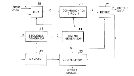
Fig. 2 is a block diagram of a communication circuit fault detector for testing
a uni-directional communication circuit.
Fig. 3 is a timing diagram illustrating the operation of the communication
circuit fault detector in Fig. 2 for the case n = 2.
Fig. 4 is a block diagram of a communication circuit fault detector for testing
a bi-directional communication circuit.
Fig. 5 is a timing diagram illustrating the operation of the communication
circuit fault detector in Fig. 4 for the case n = 1.
Fig. 6 is a timing diagram illustrating the operation of the communication
circuit fault detector in Fig. 4 for the case n = 3.
DETAILED DESCRIPI'ION OF THE INVENTION
The invention will be described by showing two embodiments of the
communication circuit fault detector of the present invention. The first, illustrated in
Figs. 2 and 3, tests a uni-directional communication circuit. The second, illustrated
in Figs. 4, 5, and 6, tests a bi-directional communication circuit.
Fig. I is a block diagram illustrating the general type of apparatus to which
3b
CA 02017~79 1998-02-04
the invention is applicable. A first data processing apparatus 1 communicates with a
second data processing apparatus 3 via a pair of signal lines indicated by arrows (a
and b). The first data processing apparatus 1 comprises a plurality of printed circuit
boards S which communicate with each other by further signal lines, also indicated
by arrows. Each signal line originates at a transmitting circuit 7 comprising, for
example, a first-in-first-out shift register, and terminates at a receiving circuit 9
which may likewise comprise a first-in-first-out shift register. The purpose of the
invention is to test the transmitting and receiving circuits 7 and 9 without halting
communication between the printed circuit boards 5, or between the first data
processing apparatus 1 and second data processing apparatus 3.
The printed circuit boards 5 contain components such as memory and
processor devices for performing data processing functions. Although not explicitly
shown in the drawing, these components may communicate with one another by
means of additional transmitting and receiving circuits, which can also be tested using
the present invention.
The first communication circuit fault detector to be described tests a uni-
dlrechonal commumcatlon clrcult,
FB923
which moves data in a single direction at a certaincommunication rate f, such as 9600 bits per second. The
communication circuit may include a single transmitting
circuit 7 or a single receiving circuit 9 in Fig. 1.
Alternatively, the communication circuit may comprise a
transmitting circuit, a receiving circuit, and their
interconnecting signal line, particularly when the
transmitting and receiving circuits are located on the same
printed circuit board.
With reference to Fig. 2, the communication circuit 11
is coupled to a timing generator 13 which generates first,
second, and third clock signals C, E, and G. The first
clock signal C has a frequency f/n equal to the
communication rate f divided by a positive integer n. The
second clock signal E has a frequency of 2-f. The third
clock signal G has the same frequency (f/n) as the first
clock signal.
The first clock signal C is supplied to a sequence
generator 15, which generates a test signal B comprising a
certain bit sequence, bits being generated at the rate f/n.
The first clock signal C is also supplied to a memory
circuit 17 which is coupled to the sequence generator and
temporarily stores the test signal. If it is only necessary
to store one test bit at a time, the memory circuit li may
comprise a simple latch. If it is necessary to store more
2~ 7~9 EB923
than one bit at a time, the memory circuit 17 may comprise a
first-in-first-out shift register.
The first clock signal C is furthermore supplied to a
multiplexer 19, which is coupled to the sequence generator
15 and the communication circuit 11, and also receives the
input data signal A to be passed through the communication
circuit 11. The multiplexer 19 is a standard two-to-one
multiplexer that multiplexes the input data signal A and the
test signal B into the communication circuit 11. The
multiplexer 19 selects the input data signal A when the
first clock signal C is in, for example, the low state,
selects the test signal B when the first clock signal C is
in the high state, and passes the selected signal to the
communication circuit 11 as a multiplexed signal D.
The second clock signal E is supplied to the
communication circuit 11 and drives the communication
circuit 11 at twice the communication rate f. Thus the
communication circuit 11 samples the multiplexed signal D at
intervals of 0.5/f, and produces an output signal F having a
bit rate of 2-f.
The third clock slgnal G is supplied to a der~lul~iplexer
21, wh~ch is cGupled to the commun,cation ~ircutt 1l and
demultiplexes the output signal F from the communication
circuit 11, producing an output data signal H and a returned
test signal I. When the third clock signal is in, for
. 2~17~7~ FB923
example, the low state, the demultiplexer 21 connects the
OUtpllt signal F to the output data signal line ll, while the
returned test signal I retains its previous value. When the
third clock signal is in the high state, the demultiplexer
21 connects the output signal F to the returned test signal
line I, while the output data signal H retains its previous
value.
The third clock signal G is a]so supplied to a
comparator Z3, which is coupled to the memory circuit 17 and
the demultiplexer 21. At each cycle of the third clock
signal G the comparator 23 compares the returned test signal
I with the test signal stored in the memory circuit 17 and
generates a result signal indicating whether the returned
test signal matches the stored test signal.
The operation of this communication circuit fault
detector will next be described for the case in which n = 2.
If the communication rate is 9600 bits per second, for
example, then the first and third clock signals have
frequencies of 4800Hz and the second clock signal has a
frequency of 19,2001~z. The sequence generator 15 produces
test signals at the rate 4800 bits per second. The
communic2tion circu~t 11 wl~l be shown as haYing a delay ~-f
one cycle of the second clock signal E. The memory circuit
17 will be a latch that stores one test bit.
With reference to Fig. 3, the input data signal A
~ FB923
comprises a series of bits (l, 2, 3, ...) and the test
signal B comprises a series of bits (a, b, c, ...). The
first clock signal C is a pulse signal comprising high
pulses with a width of 0.5/f. The sequence generator 15
generates a new test bit at the falling edge of each pulse
of the first clock signal C. The memory circuit 17 latches
each test bit on the rising edge of the first clock signal
C, producing as output the signal shown at J.
The multiplexer 19 selects the input data signal A when
the first clock signal C is low and the test signal when the
first clock signal C is high, thus producing the multiplexed
signal shown at D in Fig. 3. The communication circuit 11
samples the multiplexed signal D on each rising edge of the
second clock signal E and produces the sampled data, after
an internal delay of one clock cycle, as the output signal
F.
The third clock signal G is a pulse signal similar to
the first clock signal C, comprising high pulses with a
width of 0.5/f, but lagging the first clock signal C in
phase. The phzse lag in this case is 1.5 cycles of the
second clock E, compensating for the sampling delay and
internal delay of the communlcation circuit '~1. The
demultiplexer 21 demultiplexes the output signal F according
to the third clock signal G, producing the output data
signal 1l and returned test signal I.
7 ~
The comparator 23 operates on the falling edge of the
third clock signal G, sampling the returned test signal I and
the memory output J at this time, comparing them, and
producing a result signal that indicates whether they match.
The result signal can be furnished to a circuit, not shown in
the drawings, that initiates an error-handling action when the
returned test signal I and memory output J fail to match.
The testing operation described above in no way
interferes with normal data communication. The output data
signal H is the same as it would be if the multiplexer 19, the
demultiplexer 21, and the other test circuits were removed and
the communication circuit 11 were clocked at the normal rate
f. The test can accordingly be performed constantly during
normal communication, so that faults will be detected as soon
as they occur, greatly enhancing the reliability of the
communication circuit. The detector operates regardless of
whether the input data signal includes or excludes a
synchronization pattern.
Next a communication circuit fault detector will be
described for testing a bi-directional communication circuit
comprising a transmitting circuit for transferring data in one
direction and a receiving circuit for transferring data in the
other direction. For example, the communication circuit may
comprise the transmitting circuit 7 and the receiving circuit
9 in the second data processing apparatus 3 shown in Fig. 1.
.~
CA 02017~79 1998-02-04
With reference to Fig. 4, the transmitting circuit 31 and receiving circuit 33
are connected to a timing generator 35 that generates first, second, third, fourth,
fifth, and sixth clock signals M, O, Q, T, V, and X. The first and third clock
signals M and Q are similar to the first and third clock signals in Fig. 2, having
frequencies of f/n, where f is the normal communication rate and n is a positive
integer. The fourth and sixth clock signals T and X also have frequencies of f/n.
The first, third, fourth, and sixth clock signals are all pulse signals comprising high
pulses with a width of O.S/f. The second and fifth clock signals O and V have
frequencies of 2 f.
The first clock signal M is supplied to a sequence generator 15, a memory
circuit 17, and a first multiplexer 37 similar to the sequence generator 15, memory
circuit 17, and multiplexer 19 in Fig. 2. The first multiplexer 37 receives an input
transmit signal K and a test signal L from the sequence generator 15 and multiplexes
them into the transmitting circuit 31 by selecting the input transmit signal K when the
first clock signal M is low and the test signal L when the first clock signal M is high,
thus producing a fist multiplexed signal N.
The second clock signal O is supplied to the transmitting circuit 31, driving
the transmitting circuit 31 at twice the communication rate f. From the first
FB923
2017~
multlplexed signal N the transmitting circuit 31 thus
produces an output signal P with a bit rate of 2-f.
The third clock signal Q is supplied to a first
demultiplexer 39 which demultiplexes the output signal P
from the transmitting circuit 31, producing an output
transmit signal and a loop-back signal R.
The fourth clock signal T is supplied to a second
multiplexer 41. The second multiplexer 41 receives an input
receive signal S and the loop-back signal R from the first
demultiplexer 39 and multiplexes them into the receiving
circuit 33 by selecting the input receive signal S when the
fourth clock signal T is low and the loop-back signal R when
the fourth clock signal T is high, thus producing a second
multiplexed signal U.
The fifth clock signal V is supplied to the receiving
circuit 33, driving the receiving circuit 33 at twice the
communication rate f. From the second multiplexed signal U,
the receiving circuit 33 produces an output signal W with a
bit rate of 2-f.
The sixth clock signal X is supplied to a second
demultiplexer 43 which demultiplexes the output W from the
receiving circuit. 33 to produce an output recelve signal and
a returned test signal Y. The sixth clock signal X is also
supplied to a comparator 23 similar to the comparator 23 in
Fig. 2, which compares the returned test signal Y with the
11
2017~9 FB923
output Z from the memory circuit 17 and generates a result
signal indicating whether the two signals match.
The operation of this communication circuit fault
detector will be illustrated for two cases: one in which
n = 1, and another in which n = 3.
The n = 1 case is shown in Fig. 5. If the
communication rate is 9600 bits per second, then the first,
third, fourth, and sixth clock signals have frequencies of
960011z while the second and fifth clock signals have
frequencies of 19,200Hz. Here the memory circuit 17 is a
two-stage shift register comprising, for example, an input
latch and an output latch connected in series. The
transmitting circuit 31 and receiving circuit 33 are simple
latch circuits with no appreciable internal delay.
The input transmit signal K and test signal L are
multiplexed as shown in Fig. 5, producing the first
multiplexed signal N. The memory circuit 17 latches the
test signal L in its input latch on the rising edge of the
first clock signal M and transfers the test signal L to its
output latch on t-he falling edge of the first clock signal
M. The output of the memory circuit 17 is thus as shown at
Z in Fig. 5.
The transmitting circuit 31 samples the first
multiplexed signal N on the rising edge of the second clock
signal 0, the sampled value immediately becoming the output
P of the transmitting circuit 31. Using the third clock
signal Q, the first multiplexer 39 demultiplexes the output
signal P to an output transmit signal (not shown in Fig. 5)
and a loop-back signal R. The second multiplexer 41
multiplexes the loop-back signal R and the input receive
signal S according to the fourth clock signal T, producing a
second multiplexed signal U.
The receiving circuit 33 samples the second multiplexed
signal U on the rising edge of the fifth clock signal V, the
sampled value immediately becoming the output W of the
receiving circuit 33. Using the sixth clock signal X, the
second demultiplexer 43 demultiplexes the output signal W to
an output receive signal (not shown in Fig. S) and a returned
test signal Y.
The comparator 23 compares the returned test signal Y
with the output Z from the memory circuit 17, the comparison
being made on the falling edge of the sixth clock signal X.
Failure of the returned test signal Y and memory output Z to
match indicates a fault in either the transmitting circuit 31
or the receiving circuit 33.
This testing operation does not interfere with data
communication in either direction. Both the transmit signal
and the receive signal pass through as they would in the
absence of the fault detector circuitry. The detector
operates regardless of whether the transmit signal includes or
excludes a synchronization pattern.
The n = 3 case is illustrated in Fig. 6. If the
13
,~
~ FB923
communication rate is 9600 bits per second, then the first,
third, fourth, and sixth clock signals have frequencies of
32001~z while the second and fifth clock signals have
frequencies of 19,200Hz. The memory circuit 17 is again a
two-stage shift register, and the transmitting circuit 31
and receiving circuit 33 are simple latch circuits with no
appreciable internal delay.
There are two differen~e~ between the n = 1 case shown
in Fig. 5 and the n = 3 case shown in Fig. 6. One
difference is that in Fig. 6, the third and fourth clock
signals Q and T are offset in phase to compensate for
sampling delays and for the phase non-alignment of the loop-
back signal R and the input receive signal S. The other
difference is that in Fig. 6 both the input and output
latches of the memory circuit 17 are triggered by the rising
edge of of the first clock signal M, so that each test
signal bit spends one full first clock cycle in the input
latch of the memory circuit 17, then one full cycle in the
output latch. The output of the memory circuit 17 therefore
appears as shown at Z in Fig. 6.
~ side from these differences, the n = 3 case operates
in the same way as the n = 1 case, the comparator 23
detecting faults by comparing the returned test signal Y
with the memory output Z on the falling edge of the sixth
clock signal X in Fig. 6. Further description wlll be
14
Z01~79
FB923
omitted. As in the n = 1 case, there is no interference
with normal data communication.
The transmitting circuit 31 and receiving circuit 33 in
Fig. 4 have been described as simple latch circuits with no
internal delay, but they may also comprise first-in-first-
out shift registers of arbitrary length, the memory circuit
17 and the phase re]ationships of the clock signals being
modified accordingly.
The clock signals furnished to the multiplexers and
demultiplexers have been described as having steady, equal
frequencies, but with long first-in-first-out shift
registers, burst clocking can be employed by supplying
different clock frequencies at different times. The
multiplexer and demultiplexer burst rates may differ,
although the long-term average rates must still be equal.
Figs. 3, 5, and 6 have illustrated cases of n = 1, 2,
and 3, but it will be apparent that with a suitable memory
circuit 17 and suitable phase relationships among the clock
signals, n can be any positive integer. In particular, an
inexpensive low-speed sequence generator 15 can be used to
test communication circuits operating at a variety of higher
csmmunication rates.
Although the memory circuit 17 is shown in Figs. 2 and
4 as a separate component, it can be integrated with either
the sequence generator 15 or the comparator 23. A one-bit
~017~7~
~B923
memory can be reallzed as an input latch, trlggered by the
first clock signal, in the comparator 23. Alternatlvely, if
the sequence generator 15 uses a shift register as its
output circult, then a multiple-bit memory circuit 17 can be
realized by using the final bit position in the shift
register as the memory output, and the output from a
preceding bit position as the test signal.
Other modifications of an obvious nature can also be
made to the detectors described above without departing from
the spirit and scope of the invention, which should be
determined solely according to the appended claims.