Note: Descriptions are shown in the official language in which they were submitted.
-- 201901~
,
0 7548
Title: OPTICAL READ SYSTEM AND IMMUNOASSAY METHOD
BACKGROUND OF THE INVENTION
This invention relates to fluorometers and,
~lore particularly, it concerns a low-cost and yet highly
effective optical system for a dual channel,
-~ltraviolet-visible, fluorometer in an immunoassay
instrument and an associated method of fluorescence
spectroscopy.
Fluorometers have gained wide acceptance for
clinical analysis of blood and other biological fluids.
Conventionally, fluorometers employ an optical system
to subject a fluid sample, or a sample containing a
fluorescent dye or tag material, to light energy at a
first wavelength and cause emission of fluorescent light
at a longer wavelength from the sample. The intensity
of fluorescent emission is indicative of the presence or
quantity of a substance in the sample under investi-
gation. Because the amount of light absorbed and
emitted by such biological fluid samples is low,
conventional fluorometers are equipped with either one
or both of a high output ultraviolet light source and a
photomultiplier tube in order to achieve reliable test
results.
High output ultraviolet light sources such as
xenon arc lamps or lasers are not only expensive, but
also suffer from drawbacks such as producing excessive
heat, causing irreversible damage to specimens, creating
noise, bleaching fluorescent tag materials, and
re~uiring complex and expensive control systems. While
-
'- 201gOl~
--2--
- o it is known in the art to use a less expensive,
relatively low ultraviolet output, broadband light
source, such as a tungsten halogen lamp, and filter the
lamp output with an ultraviolet transmitting bandpass
; filter, the resulting filtered radiation is of such a
low level that the fluorescent light emitted by the
sample is difficult to detect. Heretofore, the dif-
ficulty of fluorescent light detection has been ad-
dressed exclusively by the use of an extremely sensitive
photomultiplier tube to detect the low levels of sample
emitted fluorescence. While providing for radiation
detection even at the photon counting level,
photomultiplier tubes are expensive and fragile and
necessitate relatively complex control circuitry.
In light of the foregoing, there is a need for
an improved optical fluorometer system which provides
the desired analysis without requiring the use of high
ultraviolet output light sources and photomultipliers.
20l9~15
--3--
O SU~IARY OF THE INVENTION
In accordance with the present invention, an
optical system for a fluorometer is provided by which
reliable dual channel fluoroanalysis is effected using
low cost components.
In a preferred embodiment of the present
invention, a low cost and yet highly effective dual
channel fluorometer, having excitation and emission
branches, incorporates a relatively low ultraviolet
output, tungsten halogen excitation source together with
solid state photodetectors to detect the low levels of
sample emitted light encountered in fluoroanalysis.
The attainment of reliable results with such components
is made possible by incorporating optics in the excita-
tion and emission branches that are approximately 90
percent transmissive in the ultraviolet region to
maximize throughput and by using solid state circuitry
together with a filter wheel having both light blocking
and light passing regions in a manner which fully
accounts for dark signals associated with the solid
state photodetectors and amplifiers.
In the practice of the present invention, a
sample holder or assay element containing a biological
fluid such as blood serum is placed above a read port of
the present optical system, illumination provided by the
tungsten halogen source and filtered through an excita-
tion branch bandpass filter is focused on the front
surface of the sample holder so as to cause the par-
ticular constituent under study, or a fluorescent dye or
tag material in the sample, to fluoresce. The emitted
fluorescence is collected and directed through an
emission branch bandpass filter and focused on a
photodetector. The present optical system also includes
a reference photodetector for receiving illumination
from the tungsten halogen source and providing a signal
which is used to compensate for variations in source
output.
20 1 90 1 ~
The excltatlon and emlsslon bandpass fllters are
carrled on a fllter wheel as a dlametrlcally opposed matched
palr of fllters. The fllter wheel also lncludes a palr of
dlametrlcally opposed opaque surfaces. Wlth the fllter wheel
ln one posltlon, the excltatlon and emlsslon fllters of a
matched palr of bandpass fllters are slmultaneously placed
along the excltatlon and emlsslon paths of the system. Wlth
the fllter wheel ln another posltlon, both the excltatlon and
emlsslon branches are slmultaneously blocked by the opaque
reglons for purposes of obtalnlng photodetector/ampllfler dark
slgnals, whlch lndlcate component drlft.
The output slgnals from each of the maln and
reference photodetectors are ampllfled, converted, digltlzed,
and processed by solld state clrcultry to produce a
measurement whlch ls lndlcatlve of the concentratlon of the
agent under lnvestlgatlon. The processlng ls accompllshed by
uslng an algorlthm based on four sequentlal photodetector
slgnals, namely, a reference photodetector dark slgnal, a
reference photodetector excltatlon slgnal, a maln
photodetector emlsslon slgnal, and a maln photodetector dark
slgnal. The measurement provlded by thls algorlthm ls treated
dlfferently by the mlcroprocessor based on the partlcular type
of assay element belng used.
The lnventlon may be summarlzed, accordlng to one
broad aspect, as an optlcal system for use ln analyzlng the
concentratlon of a constltuent ln a fluld sample or the llke
by lrradlatlng the sample wlth excltatlon energy wlthln a
flrst band of wavelengths, determlnlng the amount of radlant
- 76207-2
-- 2019015
energy emltted by the sample wlthln a second band of
wavelengths, and relatlng the amount of emltted radlatlon to
the concentratlon of the constltuent under lnvestlgatlon, sald
optlcal system comprlslng: a radlatlon source for provldlng
llght to exclte the sampleS excltatlon and emlsslon optlcal
branches at least one of whlch lncludes optlcal means hlghly
transmlsslve at the wavelengths correspondlng to the llght
emltted by said radlatlon sourceS solld state photodetector
means for recelvlng radlatlon along sald emlsslon branch and
provlding an output lndlcatlve of the sample emltted
radlatlonS means posltloned along sald excltatlon branch for
selectlvely fllterlng sald radlatlon source to provlde sald
excltatlon energy wlthln the flrst band of wavelengths and
means posltloned along sald emlsslon optlcal branch for
fllterlng radlatlon from the sample such that the spectral
response of sald photodetector means ls llmlted to wavelengths
wlthln the second band of wavelengths, sald fllter means
lncludlng at least one matched palr of excltatlon and emlsslon
bandpass fllters and means for blocklng the passage of llght
along each of sald optlcal branches, sald fllter means for
selectlvely fllterlng or blocklng havlng at least flrst and
second worklng posltlons, each of sald excltatlon and emlsslon
fllters off sald at least one matched palr belng located ln
the excltatlon and emlsslons branches, respectlvely, ln sald
flrst posltlon, and each of the excltatlon and emlsslon
branches belng blocked by sald blocklng means ln sald second
posltlon.
The lnventlon may be summarlzed, accordlng to
- 4a -
76207-2
201~
another broad aspect, as an optlcal sy~tem for use ln a
fluorometrlc devlce adapted to analyze the concentratlon of a
constltuent ln a fluld sample or the llke by lrradlatlng the
sample wlth excltatlon energy wlthln a flrst band of short
wavelengths, determlnlng the amount of fluorescent radlant
energy emltted by the sample wlthln a second band of longer
wavelengths, and relatlng the amount of emltted fluorescent
radlatlon to the concentratlon of the constltuent under
lnvestlgatlon, sald optlcal system comprlslng: a tungsten
halogen source low ln ultravlolet content for provldlng llght
to exclte the sample; excltatlon and emlsslon optlcal branches
each lncludlng optlcal means hlghly transmlsslve ln the
ultravlolet reglon of the spectrum; a solld state photodlode
for recelvlng radlatlon along sald emlsslon branch and
provldlng an output lndlcatlve of the sample emltted
fluorescence; means posltloned along sald excltatlon branch
for selectlvely fllterlng sald radlatlon source to provlde
sald excltatlon energy wlthln the flrst band of short
wavelengths and means posltloned along sald emlsslon optlcal
branch for fllterlng radlatlon from the sample such that the
spectral response of gald photodetector means 18 llmlted to
wavelengths wlthln the second band of longer wavelengths.
The lnventlon may be summarlzed, accordlng to yet
another broad aspect, as a method for fluorescence
spectroscoplc analysls of a blologlcal fluld sample uslng an
optlcal system havlng a source of lllumlnatlon, excltatlon and
emlsslon optlcal branches, a reference photodetector for
recelvlng flltered excltatlon radlatlon, a maln photodetector
- 4b -
76207-2
20 1 90 1 5
for recelvlng flltered sample emltted fluorescence, and means
for selectlvely fllterlng or blocklng sald excltatlon and
emlsslon optlcal branches, comprlslng the steps of: developlng
a reference photodetector dark slgnal (F), developlng a
reference photodetector excltatlon slgnal (R), developlng a
maln photodetector emlsslon slgnal (S), developlng a maln
photodetector dark slgnal (D), and processlng sald slgnals to
produce a fluorescence measurement (N) where:
N = (S-D)/(R-F)G
and where (G) ls the galn of the maln photodetector slgnals.
A prlnclpal ob~ect of the lnventlon, therefore, ls
the provlslon of a low-cost and yet rellable optlcal system
for a multl-channel fluorometer. Another ob~ect of the
present lnventlon 18 the provlslon of such an optlcal system
whlch ls partlcularly sulted for use ln an lmmunoassay
lnstrument. Yet stlll another ob~ect of the present lnventlon
18 the use of solld state photodetectors and clrcultry ln a
manner whlch compensates for the nolse and dark slgnals
lnherent ln such photodetector/ampllflers. Other ob~ects and
further scope of appllcablllty of the present lnventlon wlll
become apparent from the detalled descrlptlon to follow, taken
- 4c -
76207-2
~ 2019~15
--5--
O in conjunction with the accompanying drawings in which
like parts are designated by like reference characters.
201901~
--6--
0 BRIEF DESCRIPTION OF THE DRAWINGS
The novel features that are considered charac-
terisitic of the present invention are set forth with
particularity herein, both as to their organization and
method of operation, together with other objects and
advantages thereof, and will be best understood from the
following description of the illustrated embodiments
when read in connection with the accompanying drawings
wherein:
Fig. 1 is a fragmentary cross section illustra-
ting the optical system of the present invention;
Fig. 2 is a reduced bottom view representingthe filter wheel of the present optical system;
Fig. 3 is a schematic cross section illustrat-
ing the radiant energy throughput of the present optical
system;
Figs. 4A-C are reduced top plan views represen-
ting the sequential positions of the filter wheel during
the use of a first pair of matched bandpass filters;
Figs. 5A-C are reduced top plan views illustra-
ting the sequential positions of the filter wheel during
the use of a second matched pair of bandpass filters;
Fig. 6 is a schematic block diagram illustra-
ting the solid state circuitry of the present optical
system;
Fig. 7 is a schematic chart representing the
spectral output of a conventional tungsten halogen
source; and
Fig. 8 is a schematic chart comparing the
signal to noise ratios of a photomultiplier tube and a
photodiode/amplifier combination.
_7_ 201901~
O DETAILED DESCRIPTION OF THE PREFERRED EMBODIMENT
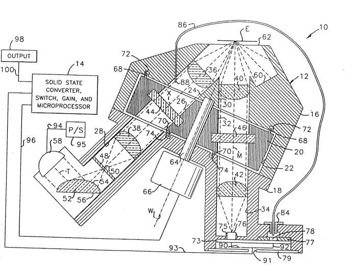
In Fig. 1 of the drawings, the optical system
of the present invention in generally designated by the
reference numeral 10 and shown to include as major
components: an optics module or head generally desig-
nated by the reference numeral 12 and a solid stateprocessing and control system 14. Optics module 12
reads a biological sample located generally at E, a
location light sealed from other components of the
instrument which are not shown.
The optics module 12 includes an upper housing
section 16 fixedly connected to a lower housing section
18 in a light tight manner. A filter wheel 20 is
rotatably supported within a corresponding cylindrical
cavity 22 in the upper housing section 16.
With the filter wheel 20 in the position shown
in Fig. 1, an excitation optical path having an optical
axis (X) is defined by a first rectangular opening 24 in
the upper housing section 16, a second rectangular
opening 26 in the filter wheel 20, and a third rectangu-
lar opening 28 in the lower housing section 18. Each of
the openings 24, 26, and 28 have substantially the same
dimensions and are coaxial with the excitation optical
axis (X). Similarly, an emission optical path having an
optical axis (M) is made up of a first rectangular
opening 30 in the upper housing section 16, a second
rectangular opening 32 in the filter wheel 20, and a
third rectangular opening 34 in the lower housing
section 18. Each of the rectangular openings 30, 32,
and 34 have substantially the same dimensions and are
coaxial along the emission optical axis (M).
Aspheric optical lenses 36, 38, 40, and 42 are
mounted within and normal to the longitudinal axis of
each of the rectangular openings 24, 28, 30, and 34,
respectively. A first matched pair of excitation and
emission bandpass filters 44 and 46 are supported in
the cylindrical openings 26 and 32 of the filter wheel
- ` 2û19~
~ -8-
o 20 normal to the excitation and emission optical axis
(X) and (M), respectively. A rectangular opaque element
48 having a small sized rectangular aperture 50 at its
center is mounted within the rectangular opening 28
transverse to the excitation optical axis (X).
Adjacent the lower end of the rectangular
opening 28 in the lower housing section 18 is a reflect-
ing and focusing element 52 having a convex refracting
front surface 54 and a mirrored plano rear surface 56.
The element 52 is positioned at an angle of 45 with
respect to the excitation optical axis (X). The lower
housing section 18 supports a replaceable tungsten
halogen bulb and integral reflector unit 58 so as to
provide radiant energy along an optical axis (T) at a
right angle with respect to the excitation optical axis
(X) and at 45 with respect to the planar rear surface
56 of the focusing and reflecting element 52.
The upper housing section 16 includes a light
trap 60 adjacent the rectangular opening 30 and opposite
the rectangular opening 24. The openings 24 and 30 and
the light trap 60 intersect at their upper ends and form
a large opening or read port 62 in the top surface of
the upper housing section 16.
The filter wheel 20 is mounted on a shaft 64
for rotation about an axis (W) which bisects the 45
angle (A) (Fig. 3) between the excitation path optical
axis (X) and the emission optical axis (M). The shaft
64 is journaled for rotation in the upper and lower
housing sections 16 and 18 in a conventional manner and
is rotatably driven by a bi-directional stepper motor
66.
The filter wheel 20 further includes upper and
lower cylindrical flanges 68 (Figs. 1 and 2) and 70
(Figs. 1, 4, and 5) which are received by corresponding
cylindrical recesses 72 and 74 in the upper and lower
housing sections 16 and 18, respectively. The cylin-
drical flanges 68, 70 and recesses 72, 74 form a light
~ 9 20~ 5
o baffling arrangement or labyrinth which optically
separates the excitation and emission optical paths and
keeps unfiltered illumination from leaking around the
filter wheel 20.
The optical system 10 further includes a main
photodetector 76 and a reference photodetector 78, each
being a conventional photodetector such as a silicon
photodiode. Both photodetectors are mounted on a common
circuit board 73 which sits in cavity formed in the
housing section 18 at the end of the emission branch of
the read head. Photodetector 76 is light sealed from
the emission branch by a light seal 75. Reference
photodetector 78 receives light from a remote section of
the excitation branch via a fiber optic 86 which is
coupled to housing 18 via a coupling 84. A light seal
77 prevents any stray light from fiber optic 86 from
entering the main photodetector 76.
Outputs from photodetectors 76 and 78 are feed
to control system 14 via lines 90 and 92, respectively,
which, for convenience, are combined as a single line 93
that passes through a single hole 91 in a cover plate
79 placed over the cavity in which the board 73 sits.
In this manner, both photodetectors are isolated from
stray light signals and experience more or less the same
environment. In addition, cover plate 79 preferably
forms part of a metallic enclosure for the photodetec-
tors to isolate them from electromagnetic interference.
The solid state control and processing cir-
cuitry 14 ta preferred embodiment of which is shown in
detail in Fig. 6) receives the output signals of
photodetectors 76 and 78 along lines 90 and 92, respec-
tively. The solid state circuitry 14 provides control
signals to the stepper motor 66 along line 96 while
light source 58 is connected to a power supply 95 via
line 94. An output device 98 such as an optical display
or printer outputs concentration levels from the solid
state circuitry 14 along a line 100.
.
20lsal~
--10--
0 As shown in Fig. 2 of the drawings, the filter
wheel 20 (shown in phantom lines) includes not only the
matched pair of excitation and emission bandpass filters
44 and 46 (Fig. 1), but also a second matched pair of
bandpass filters 102 and 104 and a pair of diametrically
opposed opaque regions or inserts 106 and 108. The
bandpass filters 44, 46, 102, and 104 are shown in solid
lines while the remaining portions of the filter wheel
20 are shown in phantom lines to make it clear that each
of the bandpass filters slants downwardly from the
exterior circumference of the wheel toward the base of
the shaft 64. Although the filter wheel 20 itself is of
a generally cylindrical design, each of the bandpass
filters 44, 46, 102, and 104 rotates about the axis (W)
in a substantially inverted conical path. In accordance
with the preferred embodiment shown in Figs. 1 and 3
where the excitation optical path and emission optical
path intersect at an acute angle (A) of 45, more or
less. The apex angle of the inverted cone corresponding
to the surface defined by each of the bandpass filters
is 135, more or less. As such, the planar upper and
lower surfaces of each bandpass filter are oriented
normal to the collimated light in each of the excitation
and emission optical paths or branches. Since the
filtering properties of each of the bandpass filters 44,
46, 102, and 104 vary with respect to the incidence
angle of the illumination to be filtered, shifts in the
central wavelength are minimized by having the filters
oriented normal to the optical path and located within
a section of the optical branch where the light is
collimated.
In accordance with the preferred embodiment,
each of the bandpass filters 44 and 46 are made entirely
of Schott absorbing glass with the excitation filter 44
passing light of a narrow bandwidth around 360 nm, and
the emission filter 46, which has a neutral density
evaporative coating, passing light of a narrow
201901~
0 bandwidth about 450 nm. In accordance with the same
embodiment, the excitation and emission bandpass filters
102 and lOs are constructed in a conventional manner as
filter packs of absorbing glasses and six cavities of
evaporative optical bandpass filters with the absorbing
glass being used primarily as a highpass filter while
the bandpass cavities are used for the specific bandpass
and sharp cutoffs. The excitation filter 102 is
designed to transmit light in a narrow bandwidth between
545 and 555 nm, while the emission bandpass filter 104
lo transmits light having wavelengths in the narrow
bandwidth from about 575 to 585 nm. It is preferred
that the diametrically opposed opaque regions 106 and
108 are defined simply by opaque sections of the filter
wheel 20 between the filters 44 and 102 and 46 and 104,
respectively. However, it is contemplated that the
opaque surfaces 106 and 108 can be opaque inserts placed
within cylindrical openings in the filter wheel 20 in
much the same way as the bandpass filters. In accor-
dance with the same preferred embodiment, the tungsten
halogen bulb and reflector unit 58 is a 35 watt tungsten
halogen bulb and integral reflector which is commercial-
ly available at low cost. The integral reflector
operates in a conventional manner to reverse the
direction of rearwardly traveling radiation from the
bulb filament, form a substantially collimated beam
which merges with the direct radiation from the bulb
filament, thereby making the most efficient use of the
output of the lamp, and is IR transmissive to remove
heat from the system. As shown in Fig. 7 of the
drawings, such a tungsten halogen bulb provides both
ultraviolet and visible radiation output. The power
output spectrum of the lamp can be calculated for
purposes of estimating and optimizing optical power
using Planck's blackbody formula.
With reference to Fig. 3 of the drawings,
combined ultraviolet and visible radiation output O from
2019015
-12-
0 the lamp and reflector combination 58 is folded and
simultaneously focused onto the aperture 50 by the
reflecting and refracting element 52. The illuminated
aperture 50, forming an object for analytical purposes,
is imaged by the pair of aspheric lenses 38 and 36 onto
a plane coincident with the signal layer of an assay
element or sample (E). The aspheric lens 38 collects
and collimates the ultraviolet and visible radiation
which passes through the aperture 50 so that it is
directed normal to the lower planar surface of the
bandpass filter 44. As such, the filtering capabilities
of the excitation bandpass filter 44 are maximized.
The filter 44 blocks the passage of substantially all
radiation having a wavelength of 390 nm or greater and
allows the passage of radiation (U) of a narrow bandwid-
th about 360 nm with a peak transmittance at approximat-
ely 370 nm. The aspheric lens 36 collects the radiation
(U) and converges it at a point (P) coincident with the
signal layer of the assay element (E). The focused
excitation radiation (P) produces specular reflection
(J) and diffuse reflection and fluorescence (H).
In order to optimize specular light control and
to reduce space requirements, the aspheric lenses 36,
38, 40, and 42 are shaved or trimmed to be rectangular
in shape so that the excitation light aimed at the assay
element (E) does not come in at too small of a raking
angle (B) with the lowest projected ray being at about
37 with respect to the assay element plane and the
angle (C) of the lowest ray of specularly reflected
light being about 33. In an effort to detect the
diffuse fluorescence given off by the assay element (E)
and to minimize spurious specular reflection signals,
the excitation optical path is directed at 45 with
respect to the plane of the assay element (E) while the
emission or detection optical path lies normal to the
plane of the assay element and the light trap 60 is
positioned to catch and absorb the specularly reflected
2~19015
-13-
0 radiation (J). Additionally, the interior surfaces of
the housing sections 16 and 18 and all of the surfaces
of the filter wheel 20 (excluding the bandpass filters)
are anodized, painted or colored flat black so as to
eliminate spurious light.
The aspheric lens 40 collects and collimates
the diffuse reflection and fluorescence (H) from the
assay element (E). The collection lens 40 is trimmed
such that the entire lens misses the specular reflec-
tions (J) off the surface of the sample element.
The emission filter 46 transmits diffuse
fluorescence (V) while rejecting or blocking any
diffusely reflecting excitation wavelengths and any
specular component (J) which may find its way into the
collection path. In accordance with the preferred
embodiment wherein the emission bandpass filter 46 is
made entirely of Schott absorbing glass, the filter 46
blocks all wavelengths of less than 425 nm and passes
a narrow bandwidth of light having a wavelength about
450 nm with a peak transmittance at about 470 nm. The
excitation and emission bandpass filters 44 and 46 are
chosen to have bandpass and absorption or "blocking"
properties for proper isolation between excitation and
emission wavelengths. Measured quantitatively, the
"blocking" factor or the ratio of incident white light
to transmitted light of the filters 44 and 46 is 10 8-
The diffuse fluorescence (V) transmitted by thebandpass filter 46 is collected and focused on the
photodetector 76 by the aspheric lens 42. To maximize
the signal at the wavelengths of interest, that is in
the ultraviolet region of the spectrum, all of the
aspheric lenses 36, 38, 40, and 42 are made of an
optical material, such as optical plastic, which is
highly transmissive at the wavelengths of interest. For
example, commercially available lenses formed of Rohm
and Haas UVT 100 Acrylic provide the desired transmit-
201g~1~
-14-
0 tance. For cost purposes, each of these lenses are of
identical construction and of conventional design.
To normalize readings to account for changes in
both the output wavelength or intensity of the tungsten
; bulb 58, optical fiber pickoff 88 is placed downstream
of the excitation filter 44 to provide a portion of the
filtered excitation light to the reference photodetector
78. As such, the output signal of the reference
detector 78 corresponds to the characteristics of the
excitation light and is used in the signal processing
algorithm to compensate for variations in bulb output.
Figs. 4A-4C depict the three sequential
positions of the filter wheel 20 during a fluorescence
analysis measurement cycle employing the first matched
pair of bandpass filters 44 and 46. Figs. 5A-5C
illustrate the three sequential positions of the filter
wheel 20 during analysis utilizing the second matched
pair of bandpass filters 102 and 104. The first and
third positions of the filter wheel 20 in both of the
sequences of Figs. 4A-4C and Figs. 5A-5C are the same.
In other words, the filter wheel 20 is in the same
position at the beginning and end of each of the
measurement cycles no matter which matched pair of
bandpass filters is being used. As shown in Figs. 4A,
4C, 5A, and 5C, the filter wheel 20 begins and ends a
measurement cycle in a position with the opaque surface
106 blocking the excitation optical path and the opaque
surface 108 blocking the emission optical path. To get
to the position shown in Fig. 4B, the filter wheel 20 is
rotated 60 counterclockwise by the stepper motor 66.
In the position shown in Fig. 4B, the excitation
bandpass filter 44 is in the excitation optical path
and the emission bandpass filter 46 is in the emission
optical path (Figs. 1-3). The filter wheel 20 is
brought to the position shown in Fig. 4C from the
position shown in Fig. 4B by driving the motor 66 so as
to rotate the filter wheel 60 in a clockwise direction.
-- 2019015
-15-
o Figs. 5A and 5C show the filter wheel 20 in the same
positions shown in Figs. 4A and 4C. The filter wheel 20
is brought to the position shown in Fig. 5B by having
the stepping motor 66 rotate the filter wheel 60
clockwise. In the position shown in Fig. 5B, the
excitation bandpass filter 102 is located in the
excitation optical path and the emission bandpass filter
104 is located in the emission optical path. The arrow
labeled (0) in each of Figs. 4A-4C and 5A-5C represents
the collimated combination of ultraviolet and visible
radiation provided by the collecting and collimating
lens 38. The arrow labeled (V) in Fig. 4B represents
the emission radiation transmitted through the filter 46
to be collected and focused by the lens 42 onto the main
photodetector 76 (Fig. 3). The arrow labeled (Z)
represents the radiant energy which is transmitted by
the bandpass filter 104 to be collected and focused on
the main photodetector 76 by the aspheric lens 42.
As shown in Fig. 6 of the drawings, the solid
state control and processing circuitry 14 of Fig. 1
includes a pair of current-to-voltage converters 110 and
112, a programmable switch 114, a programmable gain 116,
a dual slope analog-to-digital converter 118, and a
microprocessor 120. Generally, in the process for
fluorescent spectroscopy in accordance with the present
invention, current signals SC,Dc (main channel signals),
and FC,Rc (reference channel signals) from each of the
photodetectors 76 and 78, respectively, are amplified
and converted to voltage signals Sv, Dv, Fv, Rv by
passing through the converters, for example, trans-
impedance amplifiers, 110 and 112. The programmableswitch 114 provides one of the voltage signals Sv, Dv,
Fv, Rv at a time to the programmable gain amplifier 116
having an amplification which is selectable in factors
of 2 over a range from lX to 128x to produce gain
outputs gFv, gRv, GSv, GDV. The gain for each photo-
diode, (G) for the main photodiode 76 and (g) for the
-16- 2019015
0 reference photodiode 78, is selected separately. Each
of the outputs gFv, gRv, GSV, GDV from the programmable
gain 116 is fed sequentially to the dual slope A/D
converter 118 and converted to respective digital
signals (F), (R), (S), (D). The dual slope converter
118 includes, for example, a capacitor which is charged
by a signal for 700 ms. After this period, the
capacitor is discharged to a specific value. The time
required for this discharge is precisely counted. The
value of this precise count represents a digital value
corresponding to the analog input signal. The digital
values (F), (R), (S), (D) are transmitted one at a time
to the microprocessor 120 for data reduction.
More particularly and with reference again to
Figs. 4A-4C of the drawings, a fluorescence measurement
cycle employing the pair of bandpass filters 44 and 46
begins with the filter wheel in the position shown in
Fig. 4A. In this position the opaque region 106 blocks
the transmission of excitation illumination so that the
current signal Fc developed by the reference channel 78
is indicative of reference channel photodetector and
amplifier dark signals. Next, the stepper motor 66 is
driven by the microprocessor 120 so that the filter
wheel 20 assumes the position shown in Fig. 4B. In this
position, the excitation and emission bandpass fil~ers
44 and 46 are located in the excitation and emission
optical paths. As such, the reference photodetector 78
provides the current signal Rc corresponding to the
reference channel excitation signal plus dark signal,
and the main photodetector 76 provides the current
signal Sc representing the main channel emission signal
plus dark signal. Next, the microprocessor 120 drives
the stepper motor 66 so as to rotate the filter wheel 20
to the position shown in Fig. 4C. In this position, the
opaque region 108 blocks the transmission of illumina-
tion along the emission optical path so that the currentoutput Dc of the main photodetector 76 corresponds to a
- 2019015
-17-
o main channel dark signal. This cycle is repeated for
each measurement point associated with the bandpass
filters 44 and 46. A similar cycle providing for~the
development of the four photodiode current signals Fc,
Rc, Sc, and Dc but employing the filter wheel positions
shown in Figs. 5A-5C is preformed for each measurement
point employing the bandpass filter pair 102 and 104.
The start of each measurement cycle during which a
single signal is converted occurs within 250 ms of the
last cycle to minimize the effects of noise and long
term drift.
In the microprocessor 120 data reduction
provides a fluorescence measurement number N = (S-D)/(R-
F)G where (S) is the main channel emission signal, (D)
is the main channel dark signal, (R) is the reference or
fiber channel excitation signal, (F) is the reference or
fiber channel dark signal, and (G) is the gain of the of
the main detector channel.
The optical system 10 of the present invention
is particularly suited for use as a fluorometer in an
immunoassay instrument for determining antigen or
antibody concentrations using either multilayer (MTM) or
capillary (CAP) type assay elements. Capillary type
assay elements provide a diffusely fluorescent signal
which differs in wavelength from the excitation wave-
length by about 90 nm. In response to excitationradiation, each of the multilayer and capillary type
assay elements behaves like a Lambertian source and
provides a diffuse fluorescence signal whose compliance
with the Lambertian rules depends on the character of
the assay element being measured.
When analyzing a multilayer competitive type
assay element in which the conjugate, the fluorescently
labeled antibody, antigen, etc., is excited and emits
an output signal that varies in inverse relation to the
concentration of the analyte present, the multilayer
assay element is subjected to an initial fluorescence
2019~15
-18-
0 measurement cycle utilizing the opaque surfaces 106 and
108 and the matched pair of bandpass filters 102 and 104
(Figs. 5A-5C) before the fluid sample is added to the
assay element so as to produce a dry fluorescence
measurement. Then, the fluid sample is added to the
multilayer assay element, and this wet assay element is
read using the same fluorescence measurement cycle
(Figs. 5A-SC). The wet measurement is divided by the
initial dry measurement to produce a normalized multi-
layer assay element measurement which is fitted to a
calibration curve to find the corresponding analyte
concentration. Thus, when analyzing a multilayer assay
element (MTM) there is no signal differentiation. Any
background fluorescence produced by the fluid sample
itself is so insignificant in comparison to the main
fluorescent signal given off by the fluorophore adjacent
the front surface of the assay element that the back-
ground fluorescence can be ignored. For example, the
fluorescence signal produced by a blood serum sample at
the wavelength at which the element is being read is
very low and the volume of blood serum at the reading
layer of the assay element is so small that any back-
ground fluorescence contribution of the blood serum can
be neglected.
When analyzing a capillary type assay element
(CAP) in which the amount of enzyme is measured to
determine the concentration of species under assay, a
new fluorophore, such as rhodomine which does not effect
fluorescence measurements taken using the bandpass
filters 44 and 46 (Figs. 4A-4C), is added to the assay
element. It is preferred to add this new fluorophore to
the assay element substrate. However, it is contempla-
ted that this new fluorophore can be added to the fluid
sample. Fluorescence measurements are delayed a
predetermined time, for example 2~ minutes, after which
it is known that the fluorescence measurements are
changing at a fixed linear rate. Following this delay,
2019~1~
--19--.
o multiple measurements are taken at fixed intervals, such
as one minute intervals, using the opaque regions 106
and 108 and the bandpass filters 44 and 46 (Figs. 4A-
4C) and the slope of these measurement is determined.
Next, a new fluorophore fluorescence measurement is
taken using the opaque surfaces 106 and 108 and the
bandpass filters 102 and 104 (Figs. 5A-5C) and the slope
of the initial four measurements is divided by this new
fluorophore measurement to produce a normalized slope
value. This normalized slope value is related to the
concentration of the analyte under study through a
predetermined calibration curve. Background
fluorescence signals produced by the fluid sample itself
are insignificant.
In addition to the above measurements, rate
studies using, for example, MTM or CAP assays are done
by taking a series of readings at predetermined or, at
least, determinable spaced intervals.
Although it is not shown in the drawings, it is
to be understood that the microprocessor 120 monitors
the filter wheel position by monitoring the output
signals of the reference photodetector 78 and keeping
track of the rotations of the stepper motor 66.
Further, it is contemplated that the microprocessor 120
may receive additional input such as type of assay
element, filter wheel position, etc. from conventional
sensor elements such as additional photointerruptors,
proximity switches, or digital input provided by a
system user via a keyboard, numeric keypad, or touch
screen. Such input devices may form part of the optical
system, fluorometer, or analytical instrument.
Given the following equation:
P(s) = P(a) x T(1)2 x T(f) x n/(4~)
where P(s) is the power on the slide or assay element,
P(a) is the power out of the lamp in the actinic
region (53 mW MTM, 14 mW CAP),
201901~
-20-
0 T(l) is the transmission of the aspheric lenses
(0. 90),
T(f) is the transmission of the excitation filter
(0.50 MTM, 0.30 CAP), and
n is the collection solid angle of the lens (0.3).
An example optical system in accordance with
the present invention provides a P(s) ~ 550~Watts for an
MTM assay and a P(s) - 81~Watts for a CAP assay.
Also given that the minimum output of an MTM
assay element is P(e) ~ P(s) x lE-6 and for a CAP assay
element is P(e) ~ P(s) x lE-4
where P(e) is the emission signal. Then, the
power on the main photodetector of the same example
optical system is:
P(d) = P(e) x T(1)2 x T(f2) x n/(4~)
Where P(d) is the power on the detector,
T(f2) is the transmission of the emission
filter (0.50 MTM, 0.08 CAP).
Using the above equation, the minimum power on
the main photodetector developed by an MTM assay is P(d)
~ 5E-12W (5 picowatts) and by a CAP assay is P(d) - 7E-
llW (70 picowatts).
With the above values, the theoretical perfor-
mance for the present detector circuitry at 5 picowatts
of signal yields ~ 400/1 Signal to Noise Ratio (S/N),
and at 70 picowatts of signal yields ~5000/1 S/N.
As shown in Fig. 8 of the drawings and assuming
the same timing parameters, the signal to noise ratio
of a conventional silicon photodiode, such as the main
photodetector 76 of the present invention, is equal to
or greater than the signal to noise ratio of a conve-
ntional photomultiplier tube (PMT) in a signal region of
about 7 to 3,000 picowatts. Even though conventional
wisdom in the fluorometer art has been to use a photomu-
ltiplier tube for sensing low levels of sample emitted
fluorescence encountered when using a low ultraviolet
light producing source, the optical system of the
201901~
-21-
O present invention beneficially employs a tungsten
halogen bulb and solid state detectors. This is made
possible because the present optical system provides an
emission light signal of from about 7 to 3000 picowatts.
This relatively high level emission light signal
corresponds to a more than adequate signal to noise
ratio for the photodiode 76. As such, the use of solid
state photodetectors and a low cost low ultraviolet
output light source in the optical system of the present
invention provides for a low cost optical system without
compromising the reliability of the test results.
The expected signal region associated with
the use of a multilayer assay element ranges from about
4 to 3000 picowatts. The expected signal region using
a capillary type assay element ranges from about 100 to
3000 picowatts. The difference in MTM and CAP signal
regions is due in part because the fluorescence in the
multilayer element is due to the presence or absence of
tagged antigens or antibodies, while the fluorescence in
a capillary element comes from an enzyme amplification.
Thus, it will be appreciated that as a result
of the present invention, a highly effective optical
system for use in a fluorometer is provided and by which
the stated objectives, among others, are completely
fulfilled. It is contemplated that modifications and/or
changes may be made in the illustrated embodiment
without departure from the invention. For example,
while a filter wheel having two matched pairs of
bandpass filters is demonstrated in the illustrated
embodiment, a filter wheel having a greater or lesser
number of pairs of bandpass filters may be used.
Further, it will be apparent to those skilled
in the art from the foregoing description and accompany-
ing drawings that additional modifications and/or
changes may be made, again without departure from the
invention. Accordingly, it is expressly intended that
the foregoing description and accompanying drawings are
,~
- 2019015
-22-
O illustrative of a preferred embodiment only, not
limiting, and that the true spirit and scope of the
present invention be determined by reference to the
appended claims.