Note: Descriptions are shown in the official language in which they were submitted.
20 1 9525 P7786
-- 1 --
BACKGROUND OF THE INVENTION
.
1. Field of the invention:
The present invention relates to a switching
power supply device for supplying a stabilized DC
voltage to an industrial or household electronic
apparatus.
2. Description of the prior art:
Recently, in the field of manufacturing
electronic apparatuses, greater attention has been
directed toward cost reduction, compactness, higher
equipment performance, and energy saving. Accordingly,
strong needs exist for a switching power supply device
which is more compact and has higher output stability
and higher operating efficiency.
Among conventional switching power supply
devices, a self-excited flyback type switching power
supply device has been widely used, because it consists
of fewer parts and can be manufactured at a relatively
low cost. It is known, however, that the switching
frequency of such a device fluctuates depending upon
degree of the output current, with the result that
interferences occur in the operation of an associated
electronic apparatus and that a larger size rectifying
and smoothing circuit is required.
In an attempt to overcome such problems with
the prior art devices, a switching power supply device
of the regenerative control type has been proposed.
Figure 7 shows a switching power supply device of such
at type. The device of Figure 7 comprises a DC power
201 9525
P7786
-- 2 --
source 1, a transformer 3, switching elements 4 and 14,
a diode 5, a synchronizing oscillation circuit 6, a
rectifying diode 7, a smoothing capacitor 8, a secon-
dary switching element 14, and a control circuit 15.
The DC power source 1 rectifies an AC voltage
and smoothes the resulting DC voltage. Alternatively
it may consist of a battery or the like. The positive
and negative terminals of the DC power source 1 are
connected to input terminals 2 and 2', respectively.
The transformer 3 has: a primary winding 3a connected
at one terminal to the input terminal 2 and at the
other terminal to the input terminal 2' through the
switching element 4; a secondary winding 3c connected
at one terminal to an output terminal 10' and at the
other terminal to an output terminal 10 through the
rectifying diode 7; and a bias winding 3b connected at
one terminal to the input terminal 2' and at the other
terminal to the synchronizing oscillation circuit 6.
The switching element 4 turns ON or OFF in response to
ON/OFF signals which are supplied at the control termi-
nal from the synchronizing oscillation circuit 6,
thereby applying the input voltage to the primary
winding 3a and interrupting the voltage. The synchro-
nizing oscillation circuit 6 actuates the switchingelement 4 to turn ON and OFF respectively for
predetermined ON and OFF periods of time. The OFF
period continues until the polarity of the induced
voltage of the bias winding 3b is inverted. This
repeated ON/OFF cycle causes continuous oscillation.
The energy accumulated in the transformer 3
during an ON period of the switching element 4 is
201 9525
P7786
-- 3 --
released from the secondary winding 3c through the
rectifying diode 7 or the switching element 14 to the
smoothing capacitor 8 during an OFF period of the
switching element 4. After the above-mentioned energy
release, a secondary current is caused to flow
reversely from the smoothing capacitor 8 to the
secondary winding 3c through the switching element 14.
The period of this reverse flow is controlled by the
control circuit 15. The rectifier diode 7 is connected
at its anode to one terminal of the secondary
winding 3c and at its cathode to the output
terminal 10. The smoothing capacitor 8 is connected
between the output terminals 10 and 10'. The induced
voltage appearing across the secondary winding 3c is
rectified by the rectifying diode 7, and then smoothed
by the smoothing capacitor 8 to provide an output
voltage. The control circuit 15 compares the voltage
appearing across the output terminals 10 and 10' with
an internal reference voltage in order to vary the
above-mentioned flow period of the secondary current
through the secondary switching element 14.
The operation of the power supply device is
described with reference to Figure 8. In Figure 8, (a)
shows the waveform of a voltage VDs appearing across
the switching element 4; (b) the primary current ID
flowing through the primary winding 3a; (c) the wave-
form of driving pulse VG1 output from the synchronizing
oscillation circuit 6; (d) the secondary current ID
flowing through the secondary winding 3c; and (e) the
waveform of a driving pulse VG2 for the secondary
switching element 14. The hatched portions in (e) of
Figure 8 indicate reverse flow periods for causing the
201 9525
P7786
-- 4
secondary current Io to reversely flow in the secondary
winding 3c.
A magnetic flux develops in the transformer 3
as the primary current ID flows through the primary
winding 3a during an ON period of the switching
element 4 which period is determined by the
synchronizing oscillation circuit 6, so that energy is
accumulated in the transformer 3, whereupon an induced
voltage develops in the secondary winding 3c. It is so
arranged that the rectifying diode 7 is reversely
biased by the induced voltage and that the switching
element 14 remains in its OFF-position. When the
switching element 4 turns OFF in response to an OFF
signal from the synchronizing oscillation circuit 6, a
fly-back voltage develops in the primary winding 3a,
and, simultaneously, a fly-back voltage is induced in
the secondary winding 3c in such a direction that the
rectifying diode 7 is forward biased. Accordingly, the
energy accumulated in the transformer 3 is released as
a secondary current Io through the secondary
winding 3c, which is then smoothed by the smoothing
capacitor 8 and supplied as an output voltage to the
output terminals 10 and 10'. In this case, the
switching element 14 is actuated to turn ON by the
control circuit 15, but there occurs no particular
operation change, through whichever the diode 7 or the
switching element 14 the secondary current may flow.
When all the energy accumulated in the
transformer 3 is released until the secondary current
becomes zero, the voltage appearing across the
smoothing capacitor 8, that is, output voltage, is
20 1 9525
- P7786
-- 5 --
applied to the secondary winding 3c through the
switching element 14 which has been already in ON
state, and accordingly the secondary current flows
reversely from the smoothing capacitor 8, so that a
magnetic flux is generated in the reverse direction in
the transformer 3, thereby causing energy to be accumu-
lated therein. In this condition, there is no change
in the polarity of the induced voltage developing in
each winding of the transformer 3, therefore, there is
no change in the fly-back voltage in the bias winding
3b. Accordingly, the synchronizing oscillation circuit
6 causes the switching element 4 to remain in the OFF
state.
As mentioned above, the ON period of the
switching element 14 is controlled by the control
circuit 15. When the switching element 14 becomes OFF,
the induced voltage in each winding of the
transformer 3 is inverted in polarity. Therefore, the
induced voltage developing in the secondary winding 3c
causes the rectifying diode 7 to be reversely biased.
Since the switching element 14 is in the OFF state, the
secondary winding current does not flow. In the
primary winding 3a, the induced voltage develops in
such a direction that the voltage at the terminal to
which the switching element 4 is connected is negative,
and, on the other hand, the voltage at the terminal to
which input terminal 2 is connected is positive.
Therefore, the primary current flows in such a
direction that the DC power source 1 is charged through
the diode 5, so that the energy accumulated in the
transformer 3 during the OFF period is supplied to the
DC power source 1 (i.e., the power regeneration is
2019525
P7786
-- 6
conducted). At this time, the polarity of the induced
voltage developing in the bias winding 3b is also
inverted, and accordingly the synchronizing oscillation
circuit 6 actuates the switching element 4 to turn ON.
In this case, there is no particular operational
change, through whichever the diode 5 or the switching
element 4 the primary current may flow.
When all the energy accumulated in the
transformer 3 during the OFF period is released until
the primary current is reduced to zero, the primary
current flows from the DC power source 1 through the
switching element 4 which has been already in the ON
state, so that the transformer 3 is charged in the
direction contrary to the that of the above-mentioned
discharge, with the result that a magnetic flux
develops in the transformer 3 and energy is thus
accumulated therein. In this condition, there is no
change in the polarity of the induced voltages
developing in each windings of the transformer 3, and
accordingly the synchronizing oscillation circuit 6
maintains to control the switching element 4 to be kept
in the ON state.
When the switching element 4, the ON period
of which is determined by the synchronizing oscillation
circuit 6, is actuated to turn OFF, the energy accumu-
-lated in the transformer 3 is released as the secondary
current through the secondary winding 3c. Cycles of
these operations are repeated so that the output
voltage is continuously supplied across the output
terminals 10 and 10'.
20 1 9525
P7786
-- 7
The manner of performing the steady control
of the output voltage will be described. In Figure 8
showing the waveforms at various portions of the power
supply device of Figure 7, the OFF period (between
times tl and t3) of the driving pulse VGl in the
synchronizing oscillation circuit 6 is represented by
ToFF~ the reverse flow period (between times t2 and t3)
of the secondary current Io is represented by T'OFF,
the ON period (between times t3 and t5) is represented
by ToN~ and the regenerative period (between times t3
and t4) of the primary current ID is represented by
T'ON. Then, the current IoUT output from the output
terminals 10 and 10' can be expressed by:
1 1 ToFF
OUT X x X (ToFF~ 2T OFF) (1)
2 LS T
The output voltage VOuT can be expressed by:
NS TON
VouT = VIN x x --
Np TOFF
NS T'ON
= VIN x x
Np T OFF
NS ToN ~ T~ON
VIN x x (2)
Np ToFF - T'OFF
20 1 ~525
P7786
-- 8 --
The oscillation frequency f is expressed by;
f = = (3)
TON + ToFF T
In the above expressions, NS represents the number of
turns of the secondary winding 3c; Np represents the
number of turns of the primary winding 3a; LS
represents the inductance of the secondary winding 3c;
and VIN represents the input voltage supplied from the
DC power source 1.
The ON period TON is kept at a constant value
determined by the synchronizing oscillation circuit 6.
If the output voltage VOUT is constant, therefore, the
OFF period ToFF is constant, and the oscillation
frequency f is also constant. However, the reverse
flow period T'OFF may be varied by the secondary
switching element 14 controlled by the control circuit
( /2) VOUT (l/LS) (ToFF/T) in the expressiOn
(1) is constant when the output voltage Vt is constant.
Even if the output current IouT is varied, therefore,
it can be controlled by changing the reverse flow
period T'OFF. Even if the input voltage VIN is varied,
moreover, it can be controlled by changing the reverse
flow period T'OFF, as seen from the expression (2).
Therefore, the output voltage VOUT can be controlled so
as to be always kept constant by changing the reverse
flow period T'OFF. The reverse flow period T'OFF can
be changed by controlling the ON period of the
switching element 14 which is controlled by the control
circuit 15.
201 9525
P7786
_ 9
Figure 9 shows various waveforms obtained
when the output current IouT is changed. In Figure 9,
solid lines indicate waveforms obtained when the output
current IoUT flows at the maximum level from the output
terminals lO and 10', or at the so-called m~x;mum load
period, and broken lines indicate waveforms obtained
when the output current IouT is zero, or at the so-
called no-load period. When the input voltage is
constant, the ON period TON is constant, and
accordingly flux variation range a B is always constant.
In such a regenerative control type switching
power supply device, when the switching element 4 turns
OFF, a surge voltage occurs due to the leakage
inductance in the transformer 3. At the maximum load,
the level of the surge voltage is approximately the
same extent as in a conventional self-excited fly-back
type switching power supply device, and, at a light
load, the level of the surge voltage is greater than
that caused in such a self-excited fly-back type power
supply device because the peak value of primary current
is considerably higher immediately before the turn OFF.
The conventional regenerative control type switching
power supply device provides an advantage that because
of its ability to regenerate energy at the turn ON of
the switching element 4, even when a snubbing capac-
itor is connected between the both terminals of the
switching element 4, the surge voltage at the turn-on
can be efficiently restrained without involving any
turn-on loss. However, the resonance energy due to the
capacitor and the leakage inductance of the
transformer 3 is considerably great, so that ringing
waveforms are superposed over another throughout each
201 9525
- P7786
-- 10 --
OFF period, which becomes a source of noise. The
addition of a larger snubbing capacitor becomes a
greater hindrance to realization of a higher switching
frequency for compactness of the power source.
When the input DC power source is obtained
from an AC power source through a rectifying and
smoothing circuit, it is usual that the rectifying and
smoothing circuit is of the capacitor input type which
comprise a smoothing element and a capacitor and that
the capacitor is used as an input capacitor which
serves as a DC power source. Generally, it is desired
that power supply devices have a higher efficiency and
be small in size, and on the other hand the output
holding time is required to be set in order to protect
electronic apparatuses as a load from possible troubles
such as momentary interruption of input power. In the
prior art arrangement, the output holding time depends
largely upon the static capacitance of the input
capacitor, and, therefore, the static capacitance is
determined by both the power capacity of the power
source and the output holding time. For this reason,
even when there is a sufficient ripple withstand
capacity, there are cases where use of a larger input
capacitor is required. In addition, the conducting
period of the input current from the AC power source is
shorter in the stage of steady operation so that the
peak value of the input current becomes larger, thereby
causing the problem in that the power factor and
efficiency substantially drop.
20 1 9525
- P7786
-- 11 --
SU~IARY OF THE INVENTION
The switching power supply device according
to the invention, comprises a DC power source, and a
transformer having at least primary and secondary
windings, and further comprises: a first switching
means which is connected in series with said primary
winding, this series circuit being connected to the
terminals of said DC power source; a second switching
means; a capacitor which is connected in series with
said second switching means, this series circuit being
connected to the terminals of said primary winding; a
rectifying and smoothing circuit for rectifying and
smoothing a flyback voltage which generates in said
secondary winding and for outputting a resulting DC
voltage; and a drive means for driving alternately said
first and second switching means with predetermined ON-
OFF periods.
The switching power supply device according
to the invention may further comprise at least one
resonance capacitors which are connected respectively
to the terminals of at least one of said first and
second switching means and said primary and secondary
windings.
The switching power supply device according
to the invention comprising a transformer having at
least primary and secondary windings, and further
comprises: a rectifying circuit for receiving and
rectifying an AC voltage, said rectifying circuit
comprising at least one rectifying element; an input
capacitor means for smoothing the output of said
201 9525
P7786
- 12 -
rectifying circuit: a first switching means which is
connected in series with said primary winding, this
series circuit being connected to said input capacitor
means; a second switching means; a capacitor which is
connected in series with said second switching means,
this series circuit being connected to the terminals of
said primary winding; a rectifying and smoothing
circuit for rectifying and smoothing a flyback voltage
which generates in said secondary winding and for
outputting a resulting DC voltage; and a drive means
for driving alternately said first and second switching
means with predetermined ON-OFF periods.
At least one of said first and second
switching means may comprise a switching element and a
diode means which are connected in parallel.
Alternatively, said transformer further has a
bias winding, and said driving means comprises: a first
control means for driving said first switching means,
said first control means being connected to said bias
winding; and said and a second control means for
driving said second switching means, said second
control means being connected to the output terminals.
Thus, the invention described herein makes
possible the objectives of:
(1) providing a switching power supply device which can
efficiently inhibit any possible surge voltage and/or
ringing waveform at the turn-off of the switching
element, without detriment to the advantageous
characteristics of the regenerative control type
201 ~525
P7786
- 13 -
switching power supply device such that variations in
switching frequency due to changes in load can be
suppressed;
(2) providing a switching power supply device which can
effectively reduce any possible switching noise; and
(3) providing a switching power supply device which can
reduce the static capacitance of the input capacitor
without shortening the output holding time and thus
broaden the conduction period of the input current.
BRIEF DESCRIPTION OF THE DRAWINGS
This invention may be better understood and
its numerous objects and advantages will become appar-
ent to those skilled in the art by reference to the
accompanying drawings as follows:
Figure 1 is a circuit diagram of a power
supply device according to the invention.
Figure 2 shows waveforms at various portions
of the device of Figure 1.
Figure 3 is another circuit diagram of a
power supply device according to the invention.
Figure 4 is a further circuit diagram of a
power supply device according to the invention.
20 1 9525
P7786
- 14 -
Figure 5 is a graph showing the variation of
the input and output voltages of the device of
Figure 4.
Figure 6 shows waveforms of the input voltage
and the input current of the device of Figure 4.
Figure 7 is a circuit diagram of a
conventional power supply device.
Figures 8 and 9 show waveforms of various
portions of the device of Figure 7.
DESCRIPTION OF THE ~K~ KK~ EMBODIMENTS
According to the invention, even if the
potential of the first switching means is raised as a
result of the turn-off of the switching means, the
potential is clamped by the second switching means and
the capacitor, and accordingly the occurrence of any
surge voltage is inhibited. In addition, since the
second switching means is ON at that time, the voltage
present across the capacitor is applied to the primary
winding of the transformer, there being little or no
possibility of ringing occurrence.
According to the invention, the resonance
capacitor connected to the switching means or to the
both terminals of the switching means resonates with
the leakage inductance of the transformer during the
turn-on or turn-off operation, thereby lowering the
rate of variation of the operating voltage, so that the
level of switching noise can be reduced.
201 9525
P7786
- 15 -
Moreover, the energy accumulated in the
capacitor connected in series with the second switching
means to the terminals of the primary winding of the
transformer is released from the secondary winding
through the transformer during each ON period of the
second switching means, and therefore, longer output
holding time can be obtained as compared with the prior
art arrangement.
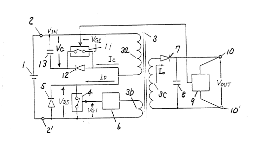
Figure 1 shows a switching power supply
device according to the invention. In Figure 1,
elements equivalent to those in Figure 7 are designated
by like reference numerals, and their detailed
description is omitted. The device of Figure 1
comprises a DC power source 1, a transformer 3, a
switching element 4, a diode 5, a rectifying diode 7, a
synchronizing oscillation circuit 6, a smoothing
capacitor 8, and a control circuit 9. The switching
element 4 and the diode 5 are connected in parallel,
and constitute the first switching means. The
switching element 4 is controlled by the synchronizing
oscillation circuit 6. The rectifying diode 7 and the
smoothing capacitor 8 constitute the rectifying and
smoothing circuit. The transformer 3 comprises a
primary winding 3a, a secondary winding 3c, and a bias
winding 3b. The device of Figure 1 further comprises
another switching element 11 which is controlled by the
control circuit 9, another diode 12, and a
capacitor 13. The switching element 11 and the
diode 12 are connected in parallel, and constitute the
second switching means. The control circuit 9 has
input portions connected respectively to output
terminals 10 and lO'. The input portions of the
20 1 9525
P7786
- 16 -
control circuit 9 are electrically separated from the
output portions connected to the switching element 11.
The operation of the switching power supply
device will be described with reference to Figure 2 in
which waveforms at various portions of the device are
shown.
In Figure 2, (a) shows the waveform of a
voltage VDs present across the switching element 4; (b)
a primary current ID flowing through the switching
element 4 or the diode 5; (c) the waveform of a driving
pulse VGl output from the synchronizing oscillation
circuit 6; (d) a primary current Ic flowing through the
switching element 11 or the diode 12; (e) the waveform
of a driving pulse VG2 for the switching element 11;
(f) a secondary current Io flowing through the
secondary winding 3c; and (g) the variation in the
magnetic flux ~ of the transformer 3.
As the primary current ID flows through the
primary winding 3a during an ON period of the switching
element 4 which period is determined by the synchro-
nizing oscillation circuit 6, a magnetic flux develops
in the transformer 3 so that energy is accumulated in
the transformer 3, whereupon an induced voltage
develops in the secondary winding 3c. The secondary
winding 3c is wound in such a manner that the
rectifying diode 7 is reversely biased by this induced
voltage. It is so arranged that the diode 12 in the
primary side is reversely biased by this induced
voltage, and also that the switching element 11 is
controlled so as to remain in its OFF-position under
201 q525
P7786
- 17 -
this condition. When the switching element 4 turns OFF
in response to an OFF signal from the synchronizing
oscillation circuit 6, a flyback voltage develops in
the primary winding 3a, and the diode 12 is forward
biased. Simultaneously, a flyback voltage is induced
also in the secondary winding 3c in such a direction
that the rectifying diode 7 is forward biased.
Accordingly, the energy accumulated in the
transformer 3 is released as a primary current Ic
through the primary winding 3a and the diode 12 and
also as a secondary current Io through the secondary
winding 3c. The primary current Ic is then smoothed by
the capacitor 13 to be supplied as a DC voltage Vc, and
the secondary current Io is smoothed by the smoothing
capacitor 8 to be supplied as an output voltage to the
output terminals 10 and 10'. In this case, the
switching element 11 is actuated to turn ON by the
control circuit 9, but there occurs no particular
operation change, through whichever the diode 12 or the
switching element 11 the primary current Ic may flow.
When capacitance components such as a
parasitic capacitance are not considered, the energy
accumulated in the transformer 3 begins to be released
first from the primary winding 3a under the influence
of the leakage inductance, at the voltage reverse in
each windings of the transformer 3 caused by the OFF
operation of the switching element 4. That is, the
primary current Ic begins to flow with the initial
value which coincides with the final value Ip of the
primary current current ID, while the secondary
current Io rises from zero. In this case, the magnetic
flux ~ in the transformer 3 decreases linearly, because
201 ~525
P7786
- 18 -
the accumulated energy in the transformer 3 is released
while the DC voltage Vc is applied to the primary
winding 3a. Accordingly, the primary current Ic
decreases monotonously until it is finally reduced to
O Amp. Thereafter, since the switching element 11 is
in the ON state, the discharge current from the
capacitor 13 begins to flow to the primary winding 3a
through the switching element 11. Since the DC
voltage Vc is applied to the primary winding 3a, the
10 rectifying diode 7 is forward biased, so that the
secondary current Io continues to flow.
After the energy accumulated in the
transformer 3 has been completely released while the
15 switching element 4 is ON, the DC voltage Vc remains to
be applied by the switching element 11, whereby the
transformer 3 is reversely excited and energy is
accumulated therein in the inverse direction. When the
switching element 11 is turned OFF by the control
20 circuit 9, the voltages of the windings of the
transformer 3 are inverted, and the rectifying diode 7
is reverse-biased, so that the flow of secondary
current Io is ceased. Thus, the induced voltage in the
primary winding 3a has a direction such that the
polarity at the terminal to which the switching
element 4 is connected is negative and the polarity at
the terminal to which the input terminal 2 is connected
is made positive. Accordingly, primary current ID
flows through the diode 5 in a direction that the DC
power source 1 is charged, whereby the energy
accumulated in the transformer 3 during the OFF period
is supplied to the DC power source 1 for power
regeneration. In this case, the polarity of the
201 ~525
- P7786
-- 19 --
induced voltage developing in the bias winding 3b is
also inverted, and, accordingly, the synchronizing
oscillation circuit 6 actuates the switching element 4
to turn ON; it is noted, however, that there is no
particular change in operation, through whichever the
switching element 4 or the diode 5 the primary
current ID may flow.
When all the energy accumulated in the
transformer 3 during the OFF period is released until
the primary current is reduced to zero, the primary
current ID flows from the DC power source 1 through the
switching element 4 which is already in the ON state,
in the direction opposite to the direction of the
discharge, so that magnetic flux develops in the
transformer 3, thereby accumulating energy therein. In
this condition, there is no change in the polarity of
the induced voltage developing in each windings of the
transformer 3, and the switching element 4 is kept in
the ON state by the synchronizing oscillation
circuit 6. When the switching element 4 operating in
ON intervals as determined by the synchronizing
oscillation circuit 6 is turned OFF, the energy
accumulated in the transformer 3 is released through
the primary winding 3a to the capacitor 13, and is also
released as the secondary current Io through the
secondary winding 3c to the output. Through repetition
of cycles of these operations the output voltage is
continuously supplied from the output terminals 10 and
10'.
The manner of performing the steady control
of the output voltage in the device of Figure 1 will be
201 ~525
- P7786
- 20 -
described. In Figure 2 showing the waveforms at
various portions of the power supply device of
Figure l, the OFF period (between times tl and t3) of
the driving pulse VGl in the synchronizing oscillation
circuit 6 is represented by ToFF~ the period (between
times t2 and t3) of reverse-exciting the transformer 3
is represented by T'OFF, the ON period (between
times t3 and t5) is represented by ToN~ and the
regenerative period (between times t3 and t4) of the
primary current ID is represented by T'ON.
During the steady operation of the switching
power supply device of the embodiment, there is little
or no fluctuation in the DC voltage Vc because the
capacity of the capacitor 13 is sufficiently large.
The primary current Ic in the OFF period which is a
ripple current is equal in both the charging and
discharge periods, with the average current of 0 Amp.
Therefore, the energy which is emitted from the
secondary winding 3c and supplied from the output
terminals lO and lO' is equal to the difference between
the energy accumulated in the transformer 3 during the
ON period and the energy supplied to the DC power
source l for regeneration during the period T'ON The
DC voltage Vc is expressed by the following expression:
TON
Vc = X VIN
ToFF
T'ON
= X VIN
T OFF
201 9525
- P7786
- 21 -
This becomes when, in the operation for stabilization
of the output voltage as already described with respect
to the prior art regenerative control type switching
power supply device, the DC voltage Vc is considered to
be a no-load output voltage.
Further, from the fact that the output
voltage VOUT in the switching power supply device of
the embodiment is obtained by rectifying the flyback
voltage of the secondary winding 3c, the following
relation is obtained:
NS
VOUT X Vc
Np
Thus, it will be found that the output voltage VOUT can
be regulated by adjusting the DC voltage Vc. For
example, when the output current IoUT has been
decreased and in turn the output voltage VOUT has
risen, the ON period of the switching element 11 (i.e.,
the OFF period ToFF of the switching element 4) is made
longer by the control circuit 9, so the amount of
outgoing charge in the capacitor 13 becomes greater
than the amount of incoming charge, with the result
that the DC voltage Vc is reduced. As the DC
voltage Vc decreases, the output voltage VOUT also
decreases, and the voltage Vc developed in and applied
to the windings of the transformer 3 drops. Therefore,
the gradient of the primary current IC is moderated so
that the DC voltage Vc finally reaches a level at which
the output voltage VOUT becomes a predetermined value.
That is, the output voltage VOUT can be stabilized by
201 9525
P7786
- 22 -
regulating the ON period of the switching element 11.
Primarily, there is no much room for variation of the
DC voltage Vc for the purpose of correcting the
fluctuation (load regulation) of the output
voltage VOuT due to the fluctuation of the output
current IOUT If the ON period TON is constant,
therefore, the OFF period ToFF is little liable to
variation, and the switching frequency and magnetic
flux variation range ~ B are generally constant as
well. General aspects in this regard are shown by
broken lines in Figure 2.
Another embodiment of the invention will
described with reference to Figure 3. The embodiment
of Figure 3 has a similar construction as that of the
embodiment of Figure 1 except that a capacitor 16 is
connected in parallel with diode 5 and another
capacitor 17 is disposed so as to bridge the terminaLs
of the secondary winding 3c. The capacitors 16 and 17
function as resonance capacitors. By connecting the
resonance capacitor 16 to the switching element 4 as
shown in Figure 3, it is possible to moderate possible
rapid rise of the voltage waveform at each turn-off of
the switching element 4. The switching power supply
device of the embodiment has a similar power
regeneration as that of the afore-described prior art
regenerative type switching power supply device. The
electric charge accumulated in the resonance
capacitor 16 is supplied to the DC power source 1 for
power regeneration during the turn-off period of the
switching element 11, and therefore it is not reduced
to a turn-on loss at the switching element 4. The
resonance capacitor 17 connected to both terminals of
201 9525
- P7786
- 23 -
the secondary wiring 3c can suppress a surge voltage
which may develop across the rectifying diode 7 with
the steep decrease to O Amp. of the secondary
current Io at the turn-off of the switching element 11.
Operations other than those in transition stages are
the same as those before described with respect to the
embodiment of Figure 1, and therefore their description
is omitted.
The addition of these resonance capacitors
has the effect that in transition stages, there will
occur changes in the output impedance of each windings
of the transformer 3 and, more particularly, during the
OFF period of the switching element 4 there will be
some change in the initial value of the current in each
windings. However, this little affects the control
operation, and rather produces an advantage in that the
peak value of the primary current IC during the OFF
period is lowered so that current loss is lowered as a
whole.
The resonance capacitor 16 may be connected
to both terminals of the primary windings 3a or both
terminals of the switching element 11. In either case,
similar excellent effects can be obtained as well. The
resonance capacitor 17 may be connected to both
terminals of the rectifying diode 7, in which case
similar effects can be obtained as well.
In the above-described embodiments, the ON
period TON is fixed, and the output voltage VOuT is
stabilized by regulating the OFF period TOFF-
Alternatively, the OFF period ToFF is fixed, and the
201 9525
- P7786
- 24 -
output voltage VOuT is stabilized by regulating the ON
period ToN~ Further, it is also possible that the
switching cycle (ToN + ToFF) of both the switching
elements 4 and 11 is fixed, and the output voltage VOuT
is stabilized by regulating the ON/OFF ratio. In any
of the above mentioned ways, the invention can be
carried out with same effect.
Figure 4 shows a further switching power
supply device according to the invention. The
embodiment of Figure 4 comprises a full-wave rectifier
circuit 19, an input capacitor 20 which is connected to
the outputs of the full-wave rectifier circuit 19, and
a control drive circuit 21. The embodiment of Figure 4
is so constructed that the DC power source can be
obtained by rectifying and smoothing AC power, and the
other components of this embodiment may be constructed
in the similar manner with those of the embodiment of
Figure 1. Namely, if the input capacitor 20 is taken
as the DC input power source 1 in Figure 1, the manner
of the operation of the third embodiment is the same as
that in the first embodiment. The control drive
circuit 21 may be constructed so that it includes the
bias winding 3b of the transformer 3, the synchronizing
oscillation circuit 6, and the control circuit 9 in
Figure 1, or alternatively it may be a circuit which
can execute such other output voltage stabilizing
methods described above. Therefore, the description of
the operation to this embodiment is omitted, and the
manner of obtaining an output holding time which is
longer as compared with that obtained in the
conventional arrangement will be described with
reference to Figure 5.
201 9525
P7786
- 25 -
In Figure 5, VOl is a set value of the DC
output voltage VOuT; Vo2 is the allowable lower limit
of the DC output voltage VOuT; Vil is a value of the DC
input voltage VIN during the steady operation; Vi2 is
the stabilized lower limit of the DC input voltage VIN
at which the control drive circuit 21 outputs to the
switching element 4 a driving pulse which has the
maximum ON/OFF ratio; and Vi3 is the halt voltage at
which the control drive circuit 21 halts. The output
holding time is a period of time from the stop of
energy supply from the AC power source and until the DC
output voltage VOuT drops to a level below the
allowable lower limit V02.
When the input is interrupted, the DC input
voltage VIN begins to drop from the value Vil, but
until it reaches the stabilized lower limit Vi2 the
output voltage VOuT maintains the set value VOl.
During this period, the operation of the embodiment is
similar to that of a conventional device. When the DC
input voltage VIN further drops to be lower than the
stabilized lower limit Vi2, the driving pulse from the
control drive circuit 21 to the switching element 4 is
fixed to the maximum ON/OFF ratio, and as the DC input
voltage drops, the output voltage VOuT begins to drop
from the set value VOl. In the conventional switching
power supply device, the output energy is supplied only
from the input capacitor 20. In contrast, according to
this embodiment, energy is also supplied from the
capacitor 13 during the OFF period of the switching
element 4, with the result that the DC input
voltage VIN and output voltage VOuT decrease at the
rates which are lower than those in the conventional
2019525
P7786
- 26 -
arrangement. In Figure 5, curves indicated by "A"
represent voltage variations in the present embodiment,
and curves indicated by "B" represents those in the
conventional arrangement. That condition continues
until the DC input voltage VIN becomes lower than the
halt voltage Vi3 so that operation is stopped. During
this course, the output voltage V0uT becomes lower than
the allowable lower limit Vo2. In this way, according
to the embodiment, the output holding time is longer
than that in the conventional arrangement.
According to the present embodiment, there-
fore, if the output holding time is to be maintained at
the same level as in the prior art device, the static
capacity of the input capacitor 20 can be decreased.
Figure 6 is a waveform diagram showing waveforms of the
DC input voltage VIN and input current Ii in the case
in which the static capacity of the input capacitor 20
is small (curves C), and the case in which the static
capacity is large (curves D). As is apparent from
Figure 6, if the input capacitor 20 which rectifies and
smoothes the AC power source can be reduced in size,
the conduction period of the input current Ii can be
lengthened so that the power factor can be improved.
Moreover, the efficiency of the device can be improved
by lowering the peak value of the input current Ii.
In the conventional regenerative control type
switching power supply device, the rectifying element
disposed at the secondary side of the transformer is
provided with the switching element, and the energy at
the secondary side is regenerated between the primary
and secondary sides of the transformer thereby
201 9525
P7786
- 27 -
stabilizing the output. In contrast, according to the
invention, a DC voltage obtained by rectifying and
smoothing a flyback voltage in the primary winding is
utilized, and the energy regeneration can be conducted
using a rectifying element which is not provided with a
switching means, whereby the output can be stabilized.
Therefore, according to the invention, without
detriment to the characteristic feature of the prior
art arrangement in that there is no fluctuation in the
switching frequency and the the magnetic flux variation
range caused by the load, the voltage present during
each OFF period of the primary side switching element
is always clamped to the sum of the input voltage and
the DC voltage, and it is thus possible to inhibit any
excessive surge voltage and/or ringing during each
turn-off period. Furthermore, the power regeneration
is carried out on the primary side only and not between
the primary side and the secondary side, so the power
regeneration can be effected efficiently without
producing loss of regenerated power due to the
transformer efficiency.
According to the invention, moreover, the
regenerative capability of the device permits the zero-
cross turn-on, and the addition of any resonance
capacitor for reducing possible turn-off loss and/or
high-frequency noise does not result in turn-on losses,
but rather inhibits ringing occurrences as already
mentioned, because the accumulated charge in the
capacitor is supplied to the input power source for
power regeneration. In particular, by the addition of
such a resonance capacitor on the secondary side of the
transformer, it is not only possible to protect the
201 9525
P7786
- 28 -
rectifying element against a surge voltage, but also
possible to lower the peak value of the primary winding
current during each OFF period. This naturally leads
to an improved efficiency and improved reliability.
Further, according to the invention, when a
DC input power source is to be obtained from an AC
power source through a rectifying circuit and an input
capacitor, the dependence on the static capacity of the
input capacitor for output holding time is reduced so
that the static capacity can be decreased, and the
conduction period of the input current from an AC power
source can be broadened. Also, the peak value of such
current can be suppressed. Thus, an excellent
switching power supply device which exhibits improved
power factor and improved efficiency can be obtained.
It is understood that various other modifica-
tions will be apparent to and can be readily made by
those skilled in the art without departing from the
scope and spirit of this invention. Accordingly, it is
not intended that the scope of the claims appended
hereto be limited to the description as set forth
herein, but rather that the claims be construed as en-
compassing all the features of patentable novelty thatreside in the present invention, including all features
that would be treated as equivalents thereof by those
skilled in the art to which this invention pertains.