Note: Descriptions are shown in the official language in which they were submitted.
PCI/US90~00939
HATRI~ CAPACITOR
BACKGROUN3 OF ~E INVENTI~N
The present invention relates generally to
c~pacltlve device3 and deals oore specifically with a high
frequency ~apacitor and a capacitor qeometry and construction
for mlnlmlzlng sèrie 5 lnductance
It is well kno~n to tho~e skilled in the art to use
capacitlve devlce~ for decouplln~ and filtering Typically
decoupllng capacitor~ store energy ~hich is returned to tne
clrcult elements upon demand to ~aintain the magnitude of the
voltage energlzlng the clrcuie e~e~cnts at a substantlally
con3tant f~xed level The functlon of the decoupling
capacltor ls to provlde the energy ~ran~fer ~ithout generatinq
noi~e and ln the ca~e of logic circuitry without introducing
loglc error~ or Jplka~ ln contrarC filcar capacitor~ ar-
gen~rally uJad to ~nunt nolse or other un~anted hign frequency
slgnal~ to grount ln Chis e~sp~ct the capaclcor accs a5 a
lo~ pa~J ~llter o~f~rlng an i~pedance path that is ~requency
dependent An analy-l~ o~ ~he c~pacitor a~ hlgh ~raqu~ncia~
ravaal~ that the capacltoe i9 equivalenc to a series
inductiva-re~lstiv~-cap-cltlve e4uivalanc circui~
Con~equently a capacltoe ls not purely cap~cltive ~ut
lnductlv- a~ ~ll and lt- p-rfor~nca - a capaciCiva davlca
~t hlghar frequoncle~ ltad dua to lts lncreased
lopadanc-
Con~ntlon~l capac~coe Con~teuction ~nd g-oo-tr~
ara ~-ll kno~n to tho~- ~klll~d ~n tna rt Ona conventlonal
fead throu~h cap-cltor n~- a ~lra ~n~cn pa~-a5 tnrouqh tne
canter of tha capacltor and ~ ter~Ln~tad co on~ and of the
capacltor ~ nt Sh- c-~- o~ ch- capacltoe ganerally
r~f~rred to a~ tha ~round Cer~inal l~ connected to tne otner
end of Cha capacitor elenant. In ~ucn a capacltoe~ only AC
currant pa~o~ through the electrod~.
.,
SU85T~TIITE SHEE~
WO90/10370 PCT/US90/00939 ~
Another well known capacitor geometry is used in the
multi-layer ceramic "MLC~ capacitor. The MLC geometry is
generally used for multiple pin connectors wherein one
electrode is grounded and a nu~ber of isolated electrodes are
connected to ~etallzed holes. The connector pins pass through
the holes in the back shell and are connected to the
capacltors making a number of feed through capacitors one for
each connector pin. Each of the capacitors has one electrode
whlch ls separate from one another ~ut all share a com~on
ground electrode,
An additional qeometry uses a capacitor ~ith t~o
lead~ connected to the internal capacitor element and i5
typically used for hlgh re~uency, lo~ effective se:ies
reslstance (~SR) capacitors in hlgh frequency po~er supplies.
~ t ls a general aim of the present invention to
provlde a capacltor geometry and s~ructure that minimi-es the
ef~ects of inductance ~y providinq a nunber of connections
across the area of the capacltor.
SUBS.~TU~E S~ F~
' ~90/10370 PCT/US90/00939
~ RY QF INVENTION
In accordance with the present invention, a multipln
matrix capacitor for use at high frequencies is presented and
lncludes a plurality of first sheets of conductive material
defining a first electrode and a second plurality of sheets of
, conductive material def~ning a second electrode ~herein the
flrst and second sheets of conductive material are stacked in
an lnterleaved arrangement and 3re separated by a dielect:lc
material to form the capaciti~a elemcnt
}n one a~pect of the ln~ention, a plurallty of first
means ln the ~orm o~ ~ins or stakes are provided and contact
each of the ~lrst sheèts of conduc.ive material and provlde
connecting means to the irs~ elecerode A plurality of
second means ln the form of pins or stakes coneact each of the
~econd sheets o f conduct~ve material and provide conneccin~
means to the second electrode T~e first and second
connecting means are disposed adlacent to one anocher in a
grid arrangement 80 that contact ~i~n the first ànd ~econd
electrodes is di~trlbuted along Che ~ur~ace of Che first and
~econd ~heets of conductive macerial to minimi2e Che
conductlon path bet~een ehe ~ir5e ànd the ~econd connèccin~
means and the first and sacond el-ctrodes respec~v-ly ~h-re~y
lnductance du~ to tha conduccion path ls su~stan~ally
ellminated The capacitor ls arranged to conducc DC currant
along the surfac~s of th- 50nd~ctor ~heets comprls~ng tne
electrodes
In ~nother a~pect of ehe inv~neion, a ~-ction of one
of the flrst and s-cond ~heeCs of th~ conducclv~ ae-rial
form~ a th~rd electrod- co provlde a 9pllc c~paclCor
In ye~ anotner asp-ct of Che lnvenelon, ona of ~he
~l~ctrodes ls m~de of ~ ~incerad cancalum matcrlal and is
enclosed ~lthin a hermet~cally sealad case wh~ch i5 flll-d
~lth an electrolyta eo form an alactrolyeic matrix capacitor
A number o~ termlnals ~re arranged ln a pin grld array eo
p-rmlt contact eo th- sintared tanc~lum alQng t~e surfaca of
the electrod~
S~SrlTUTE SHEE~
f
WO90/10370 '~' ' ' PCT/US90/00939 '--
BRIEF DESCRIPTION OF THE DRAWINÇ~
Additional features and advantages of the present
invention will become readily apparent from the following
written description and drawings wherein
~ ig, l shows the baslc seructural concept of the
interleaved foil sheets for~ing the capacitive ele~ent used in
the present inve~tion
Fig 2 is an end vieu il~ustrating a stack of inter-
leaved ~heets of the capacitlve ele~ent of Fig
Fig, 3 lllustrates cur~^nt I paths in the capacitive
element utll~zed in the capac~or a the present invention
Flg 4 illustraees sche~atLcally the equivalent
clrcult of the capacltor of Fig. ~ includlng parasitic
lnductanccs and reslstances
Flg, 5 sho~s a ~etal~z-d foil wlth marginal
~nsulatlng edges,
Fig, 6 lllustrates ehe ~eo-etry of t~e ~ctallzed
foll~ o~ Fig 5 and ln for~lng a capacltor of the present
lnventlon
Plg 7 lllustrates a capacltor made ln accordance
wlth gaomeery of rlg 6
Flg 8 lr ano~her ~bodi-ent of the pres-nt
lnventlon ~hereln the a}t~rnate la~ers of tb~ capacltors are
tabbed eo provlde a nuober of connection polnts ~long t~e
perlphery o~ the capacltor
Flg 9 lllu-tr-Ca- ~c~em-elc-lly ~ multipln, flat
plat~ capacltor e~bodylng t~e pres~n~ ~nven~on
Flg lO ls a par~l-l vl-~ o~ prlntad clrcul~ board
upon ~hlcn ~n~ aultlpln c-p~c~tor of th~ pr-~ent inven~lon ls
mountad nd conn~cead to ~n 1n~-rdLg~t~d bus
F~g 10a ls a d~gr~ lc r~pr~san~at~on of th-
matrlx capacltor ~avlng bus ~acCLonS acr~ngad to provlde aqu~l
conductlon path lang~s
rlg 10b 1~ n L~Luqtc~tion sbowln~ un~qual
conductlon paths of th~ capac~tor arrangement of ~ig lO
~ SHE~
' -90/10370 PCT/~S90/00939
,, s
Fig. 10c is an illustratlan showing equal conduction
paths for an alternate arrangement of the capacitor of Fig.
- 10.
Fig, 11 is a plan view of the capacitor of the Fig.
9,
Fig, 12 is a sec;ional vlew ta~en along the line 12-
12 of the Fig. 11.
Plg, 12a is an alternate eobod~ment of the capacito:
of Flg. 12 ant lllustrates ~ne possible interconnaction
arrangement.
Flg. 12b ls an al~ernate e~bodiment of the capac~cor
of Plg, 12 and illustrates anot~er possible interconnection
arrangement.
Plg. 1~ is a vie~ of the capacitor of ~ig. 12
mounted on a heat slnk,
Fig. 14 is a dia~ra~atic lllustration of the
capacitor o Flg. 12 arrange~ wl~h a res~stive layer and a
heat slnk to provlde a snu~ber cLrcu~e,
Flg. 15 i- a plan vlau of the snubb~r circuit o~
Pig. lq.
~ ig. 6 lllu5trates a convoluted connaccor plate
~hlch may be utlllzed co reLleve strass due co differances in
tha thQrmal expanslon of tne oaea~lals of Che capacl~or.
Plg. 1~ illuseraees dia~ra~atlcally a four ter~lnal
capacltor mounted on a naa~ sink.
~ lg. 18 ~llustrates anot~er a~od~n~ of the
capacltor of t~e pre~enc lnvenC~on.
Flg. 19 lllustrates dlagr~m~acically Cha capacltlva
l-m-nt o~ eh- pr~nC inven~L~n ~er~ln Cha pins conneccing
the alt~rnate plat-s are ^U shapa~ to handla l~rger DC
currantJ and wh~reln ~err~C~ layer ~u~rounds the ~U~ ~napad
wlre to provld~ a ~ries lnducCance ~o tha DC currenC.
Flg~ lga 15 a aleccrlcal equlvalenC clrcul~ for t~e
capacltor arran~cm~nc o~ F~g. I9.
~iB~UlE SHE~T
WO90/10370 PCT/US90/00939l- -
Fig 20 is another embodlment of the present
invention wherein the multipin capac?tor of Fig 11 includes a
section to form a split capacitor
Fig 21 is a schematlc illustration of the split
capacitor of Fig 20
Fig 22 is a sche~atic o' a symmetrical push puli
circuit using a 5plit capaci.or .llustrated in Fig 21
~ ig, 2~ is a plan view o~ a hybrid circulc substrate
upon which the circuit components ~nd the spllt capacitor of
Fig, 20 are mounted,
Fig. 24 is a plan view of the multipin capacitor of
the pre~ent lnventlon sho~lng a section removed to form a
baslc capacltive structure to accommodate various packaging
configurations
Flg, 25 ls a plan vie~ of a pln grid inline pac~age
con~lguratlon of a mulcipin capaci~or of the pres~nt
inv~ntlon,
Plg 26 1~ an end vl~ of ehe capacitor of the
Flg 25
Flg, 27 15 a plan vie~ of a pin grid in-line
capacitor whereln addltional componen~ elementq are attached
to the connectlng pln~
Fig 23 l~ an end vio~ of ehe capacitors of Fig 2
Flg. 29 15 a plan vie~ af the capacitor ~ccion of
Flg 24 rho~lng ~ho locatian of a ver~cal in-llne cut co form
a capacltive elemene tnae Oay ~e u5ed in alternaeo package
arrangem-nts
Fig 30 Jho~ th- r-~ult-nt cut rection of tlg 29
rlg 3l 1~ an nd vio~ o~ ehe capflcitoe ~-ction o~
rlg 30 ~lth l-ad~ attached to ~he capacltlv~ elem~nt
rlg 32 lr a plan vte~ of anoch~?r emcodimon~ of the
multlpln capacltor of the pr~-nt ~nvantion wher~in the
capacleor is ~n ~?lec~roly~ic cap~c~or
Flg 33 li~ 3 ~ectianal ~Lew tak~n alan~ the line 33-
33 of Flg ~2
S~SITIl~ S~E~T
.
``` :
' ~90/10370 PCT/US90/00939
Fig. 34 is another embodiment of the present
invention and iilustrates a sectional view of an electrolytic
tubular capacitor,
Fig, 35 is a cross sectional view taken along the
line of 35-35 of Fig, 34.
Flgs, 36-39 illustrates the electrolytic functional
equivalent of the capacltor of Fig. 1.
Fig, 4~ illustrates the -;ectrolytic functional
equlvalent of the capacito~ of Fig. 9.
SUBSrllUTE SHEE~
WO90/10370 PCT/US90/~939~--
DETAILED DESCRIPTION OF TNE P~EFERRED EH80DIHENTS
Turni~g now the drawin~s ~nd considering the
invention in further detail, Figs 1 and 2 illustrate the
basic geometric structure of a capac~tor embodying the pres~nt
invention, Fig 1 illustrates the ~asic construction concept
of a capacltor wherein a nu~ber of foils are interleaved by
sheets of dielectric mater:al In ~lg ~, it is seen that the
basic capacitor structure la lncludes a flrst foi} sheet ~2, a
sheet of dlelectrlc mat- lal or :~sulator 14 and ~ second foil
sheet 16 arranged so that Che dielectrie sheet material 1~
separates the folls 12 and ~6 rh~ foil sheet 12 and 16 are
substantlally ldentical to one another and are arranged in a
alternatlng pateern with each sheeC ~eing in a transverse
dlrection to another sheet such that the longltudinal
dlmenslon of one sheet is -ransverse to the long~tudinal
dimenslon of an ad~acent s~eet Tne sheet of dielectric
material 14 ls dlmensioned to be larqer than the horl20ntal
dlmenslon of the ~oi} sneecs 12 and ~6 and to ~e smaller than
the longltudlnal dlmension of the foll sheet 12 and 16
Harglnal areas 18,20 of dlelect lc material are provided in
the longltudinàl dlrectlon a~ s~ee~ '2 and marglnal araa 22,2q
dlelectrlc matorlal are provided ln tne horl20ntal directlon
of sheet 12 As can b~ seen, Che fo;l sheets 1' and 16 may ~e
lnterl~a~ed dnd 5~para~ed ~ the ~lelectrlc sheeC ~ ~o tnat
the long~tudlnal ends 26,2~ of sheet 12 extand ~yond tne
dlel-ctrlc sheet 14 and y~t a~ ~nsulated ~rom ~e foll sneet
16 In a Jlmllar mann-r, tn~ foll heet ~6 h-s longltudlnal
end~ 30,~2 ~hlch extend ~oyond C~e dlelectrlc thaet 1~ ~hlle
rom-lnlng ~nJul-t~d from tn~ ~oll sheet 12
~ ach of tha fol! sheet5 1~ may ~ electrl~ally
t~rmlnated to pro~lde connec~Lon to t~e lon~Ltudlnal nds of
th~ foll sheeCs As ltlust~at~i~ Carmlnatlons 14,~6 are mad~
to the r-~p~ctl~R lon~lcud~nat ends 3~ sheeC L~ and
termlnatlons 38,~0 are made co Che respectlve long~udlnal
ends of ~heeC 16
SUBSTlTllTE SHEFT
WO90/10370 PCT/US90/00939
,., g
Fig. 2 illustrates the alternating pattern
arrangement of Fig. 1 stacked in a parallel fashion wherein
each set of foil sheets 16,16 are shown with their respective
longitudinal ends connected to one another and terminated in
connections ~8 and 40, respectively. Similarly, longitudinal
ends of the set of foll sheets 12,12 are connected to one
another and terminated ln connection 36. It is recognized
from ~ig 2. that the stacked alternating pattern ~..angement
of foil sheets and dielect.ic sheets is similar ta ~hac of the
well-known 1at plate capacito.. Accordin~ly the
characteristics of a flat plat~ capacitor and ics associated
characterizing equatlons and rela~ionships are also applica~le
to the structure of Fig. 2 and the foll sheets may be thought
o~ as the ~plates~ of the capacitor.
Howèver, in contrast ~o Che convontlonaI flat plate
capacltor, the capacitor of the present invention may carry CC
current along the surfaces of the foil sheets form~ng ~he
capacitor wlth current en~ering OQe lonqltudinal end and
exltlng the opposlte longleudlnal end of a foil sheet. For
example, às sho~n ln Fig. 1 curr~nt I can enter the
connectlon 34 ln tne dircc~ion of arro~ 42 and exit tne
opposlte lonqltudlnal end Chrou~ the connecClon 36 'n the
dlrectlon of arrow 44. ~he conneceions 38 and ~,
respectlvely o~ the fall 5heet Io ~ay be conneceod to ground.
The current ~ that may be carriod ~y a respoctive ~oll sheet
ls llml~ed ~lnce the chlckness of t~e foll sheot ls generally
very thln. However, slnce a larqe numb~r may be connected in
parallel, the total current carried may be appreciable. ~n
addltion, the thlckness of the foll shee~ could ae increa~ed
to lmprove lts l~teral conduc~i~ley agDin p-rmlttLn~ larger
md9nltud~s of DC cùrrQnt co ~ Ch~ d. Th~ fol1 sheeCs could
also be made of ~xtend~d ~oLl ~o peev~n~ puncture ~y excessive
AC currents~ In any eVQn~ capac~tocs are generally
always ~ound and carry na OC ourcen~ thrDu~h or along the ~ilm
comprLsLng the c~pdcitar as is possi~le Ln t~e present
lnventlon.
SUBS~I~UTr SHEET
~ J~
~ i i ,~ ,,
WO 9û/10370 PCl /US90/009
Another advantage of the geometric structure of the
capacitor of the present invention is that any stray
inductance will appear in series ~lth the through current I
and substantially no stray inductance will generally appear in
series with the capacitive element. Thus, the capacitor will
exhibit better high frequency performance than conventional
capacitors,
Turnlng now to ~i~s. and 4, Pig. 3 illustrates
that both sets of foil shcecs ~ and 16,16 may be arranged
to carr~ current I to fur~her Lmpeove the throughput of tne
capacltor. As illustraced i~ ~ig. ~. current I can enter lead
34, ~low across the surface of the foil sheet ~2 and exit lead
36. ~ikewlse, current I can encer lead 38 and exit lead 40.
I~ the capacltor ls used as a decoupl~ng capacitor, leads 18
and 40 can be connected to el~ctrical ground. Fig. 4 is an
lllustration of the equlvaleQc clrcu~ of the capacitor of
Plg.
3. The capacltive elemen~ is g~nerally indicated 46 and
lllu~trates t~e re~ultan~ parasi~ic inductance and retiseance
due to the termlnatlons o~ cne leads co the foil sne~s. For
lllu~tratlvo p~rpo~es, reslscance ~ and inductance 50 are
shown as~ociated with ~ne lead conneceion 38, reslseance 52
and lnductance 54 wit~ the Lead connection 40, the res~stance
56 and lnduc~ance 58 witn ~ne }ead ;onn~ction l~ and
roJl~tance 60 and induccance 6~ ~leh ~h~ lead conneccion ~6.
~ecause the resistance and Ln~uc~ance are assoclac~d ~itn tne
parcltic~ and the tor~inations. eh~ capacltlve el~ent ~6
approaches tho charactorlst~cs o~ n ldodl capac~tor.
Tho capacitor of ~o pres~nt ln~ontion may also be
conJtructod uslng a motal~:od ~ilm to accom~oda~o applications
whoroln low DC curronts aro lnvo~ved and ~n ~hlch a nlgner
capacltance por unit of ~olu~e ls necessary. sucn a metali~od
fllm 1~ lllus~rated ln Flg. 5 and ~5 g~nqrally d~signated 62.
The ~llm 6~ ls snown w~tn ~nsu~a~ing ~-rg~nal ae~as 6~ . 66
along oacl~ longlt-ldlnal SLde~ 2~ tbe me~al~2ect film sneet is
made as a square and ebe she~ts aee alternately ae~anged so
~'
SUBSTmJTE S~EET
"~90/10370 PCT/US90/00939
11
that the insulating margin of one sheet is transverse to the
insulating margin of an adiacent sheet and the sheets are
stacked in this alternating arrangement, the construction of
the capacitor ls the equivalent of the structure illustrated
in Figs. 1 and 2. The four sides of the resulting structure
may be metalized to allow terminatlon of the metalized edges.
The entlre capacitor struc.ure may now be sealed. The
resultant capacitor geomet,y ls ~llus~rated in Fig. 6 and is
applicable to the construction o' other capacitors including
ceramlc and electrolytlc t~pas.
One method for constr~ctin~ the capacitor geometry
of Pig, 6 is lllustrated in Fig. 7 whereln a card or~ 68 is
wound wlth two colls 70 and 72 ln an interleaved fashion and
transverse to one another. Each wrap of one coil is followed
by a wrap ln a transverse direc~ion to the im~diatcly
precedlng wrap of the second coll to provide tne interleaved
arrangemont. After the colls are wrapped, the ends o~ ~ne
re~pective coils are shoared to -~pose t~e edges of the foll
~he~t~ to p~rmlt acc~s ~or ter~ina~ions. ~n tne lllu~tratlon
of Flg. 7, coll 72 ls sheared at lts respacClve ends ~ and t6
along the das~-d llnes ~8 and 80 respectlv~ly. Similarly, the
coll 70 15 also sheared at lt5 raspec~lva ends. Tne ~naared
edg~s have the samo charac~eristics as metallzed film
capacltors and may be solder 5prayad so tha~ leads mAy be
attach~d,
Th~ colls ~0,72 could also oe msde fro~ a me~ali~ed
fllm wlth in~ulating marqins or could al-o b~ made of a
combin~tion of a foll nd fllm ~ound tog~tner. ~f tno
con~tructlon ls made ~lth ~oll and film wound toqetnee ~nd
tho fllm 1~ wound wlth a gre-~er ~ansion th-n th~ foll or
alt~rnJtlv~ly, lf tne fil~ ~aco ~odoc~Cely shr~nka~L~, tne
fllm would pull back from the ~dg~s af~-r cu~ln~ eo permlt a
bQttor termlnation to be made to ~h~ foll wlndings~
Ano~hQr ~mbodlm~ne o~ ~n~ oapac~tor of tne present
inv~ntlon is lllustraCed ~n ri~. ~ and LS genQrally des~gnatcd
8'. The capacitor a~ of r~ is similar in cons~ruc~ion to
SU8STlTt3TE SHEE~
.
W090/10370 PCT/US90/00939 ~~,
12 `'`~
the capacitor of Figs. l and ~ in that foil sheets are alter-
nately stacked with a diele~tric sheet separating adjacent
foil sheets. In Fig. 8, the ca~acitor 82 includes a first
foil sheet 84 having a number of tabbed portions 86,86
extending in a direction transverse ;o the longitudinal
direction of the foil sheet 84 and ~hich tabs are arranged in
a spaced relationship with one another. ~ second tabbed foil
~heet 88 also lnclutes tabs 94,94 ~bich extend out~a~dly in a
transverse dlraction from tho long~tudinal sides of the shee~
88 ln a manner simllar tO the t3~5 ~5, 35 of the tabbed shee~
84. The tabs 94,94 are in a spaced :elationship with one
another and al~èrnate or interdigi;a~e with tabs 86,86 of the
tab ~oll sheet 84, ~n a si~il3r manner as described ln
connectlon wlth ~igs. ~ and 2, a dLelectric sheet 96 is used
to separate the alternating ta~bed film sbeets 84 a~d 88,
respectlvely as the sheets 3re stacked, The ~etal film may be
cxposed as descrlbed a~ove to perml~ termination to the tabs
of the respectlve alterna~ing Cab sheets 84 and 8g. One
advantage of th- tabbed capacl~or of Flg. 8 ls that a number
of termlnals are distrlbuced alon~ the area of the capacltor
so that any area of the capacit~t is close to a termination
polnt whlch minimiZes the lead lengehs bet~een a circuic
component and the capacltor co reduce lead lnductance. As in
the ca~e of thc capacl~o: illus~:a~ed n Fl~. 3, ~Qth sees of
foll sheets 84,88 may ~e made t~ C3r.y current t~ ~ncrease the
throughpu~ of Che capac~tor.
The capacitor 8~ of Fi~. Q is illustrated ~s lt
mlght be arranged in a deco~pling appllcatlon. One se~ of
foll sheets 88,88 have thair capacLtl~e ta~s g4.9~ connccted
to a ground r~ference poten~id}. ~he othar ~a~ of foil sheets
84,84 have thelr re~pectlve ~a~s 8~.8~ ~rrangad ~o carr~
current I ln the dlrectLon of ACrO~ 8' across Cha surfaca of
the ~oll sh~ets 8q,g4 and ouC the ~s ,~.86 oppos~te the
lnput t~bs.
~ onslderlng now ano~her em~odlment ~ the pretent
invention, Flg. 9 lllustraces d~a~ra~atlcdlly 3 f ~3~ plate
~U85mUT-c SltES
,~ ~j rJ _ __ __ _
?90/10370 PCT/US90tOO939
13 '`
multipin cap~citor as described abov- ~herein a number of
terminals or stakes are distributed along the surface area of
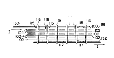
foil sheets of the capacitor. In Fig. 9, a capacitor
generally designated 98 is illustrated and comprises a number
of first plates 100,100 interleaved with a second set of
plates 102,102. Dielectric sheets 104,104 separate the
surfaces of the interleaved plates '00 and 102, respectively
a~ illustrated. Each of the plates i00,100 have a number of
openings 106,106 which extend tnrough the plate and are in
registry wlth like holes in othe~ like plates 100,10~ in ;he
interleaved stack. Similarly, places 102,102 have openings
108,108 extending through the pla~e and in reg~stration w~th
like holes 108,108 ln other like plac-s 102,10_ in the sc3ck
of interleaved plates 100,102. ~n addition, places 100.10Q
have second, s~aller openings l~O,~O which are located ln
re~lstratlon wlth holes 108.108 in oeher plaees O~ ' in c~e
lnterleaved s~t of 5tacked places. ~ikewise, places 10',102
have small holes 112,112 arranged so ChaC the holes ll~ ~ one
plate 102 are ln reglQtratlon ~ic~ ~e holes 106 of oehers
plate 100,100 in the stack o~ incer~elved plates 100,~0'. As
~llustrated in Flg. 9, cne noles IO~ and Ll~ are in
reglstratlon wlCh one anot~et a5 are c~e holes IQ~ and ~10 in
reglstratlon wlth one another. Pins or stakes ~14a. 11~,
114c and 114d are used ee cannecc plaees la~ t3 on-
another as lllustraCed ln Fi~. q. ~ike~ise, pins or scakes
116a, 116b, 116c and 116d 3re ~orced ehrough the ~1e5 1LO.110
ln the plateJ 100,100 to connect the plates to LOO ~o one
another. Tho oponing~ o~ holes LO~ aQd lO~ in th~ p1atas 100
and 10~ respectl~e1y are 1ar~ onouqn to ~eov1da su~lcianc
cle~rAnco ~or the respective p~ns ~ 6 ~cn p-S5 C~roUg~
And connect the plato~ toge~er. Pre~era~1y~ t~e dlelectrlc
rhoee 104 al80 has holas ~h~ch ae~ in ee~iste3t~0n ~lch the
holes 106, 10~, 110 and 11~ co prov1d~ cleAranc~ f~r Che
rospoctlve plns 114,116 ~hic~ pass ~hrouq~.
The dlamecer af the hale5 l L~. l lO and 11~ is
made slightly smaller than the oross sect~onal are~ af the
pln.s 114,116 50 that ~hen the pins are foec~d Chrou~h holes
lnterference fit occurs ~et~een the pins and Che plates so
SUBSTl~U~E SHEET
WO90/10370 PCT/US90/00939~'
14
that there is a contact between the recpective plate and the
associated pin which passes through. Other methods for
achieving the above result may als~ be used; for example, the
plates may be made with clearance holes in the respective
alternating plates in registration ~therein the plates are
stacked and comprèssed to for~ the s;_ucture of the capacitor.
The contact holes can then be drille~ and then the pins
inserted to provide cont3ct ~ith the associated interleaved
plates. Obviously the conea~t hoies ~re smalle- than the
clearance holes through whlch the pins pass to allo~
dlsplacement contact, Such dispiace~ent contact methads ace
well known, for example, ~nse.:Lng a square pin into a roun~
hole. A capacltor constructed in 3ccordan~e with the above
method may be sealed, encased. or reinforced.
The structure of the ~ultip~n flat plate capacltor
o~ Plg. 9 ls well sulted for use on ~ prLnted cLrcu~t board
hav1ng a ground and at least one powe: plane ~herein the plns
connected to one set o{ plates a~c connected to the po~er
plane and ehe plns connec~ed ~o the o~her set of plates are
connected to the ground plane. Fig. ~0 Ls a fraqmen~ary,
schema~lc vle~ of a mulclpln c~pacit~ and a PC board ~therein
the capacltor, generally design~ced 1~ is mounced on a
prlnted clrcult board generally ~esL~nated 12a. A ~us
generally desl~nated 122 ~hlch may ~e the po~e~ or ground
plane ls lllustrated and ~ncludes ~us sections 1~3 and 125
each of ~hlch are connected to the pLns '~4.~ hLch are
attached to one SQt of the Lncereaved platQs of the capacitor
118. The bus 122 ls ~nter~L~ltate~ so ~hat current i enterlng
one end 126 ln the dlroction of a~o~ 125 of the bus 123 flo~s
ehrough the plates of the capac~o~ conn~ceRd ~y ~h~ plns
124,124 to roach ~he bus 125 ~nd ou~ ~he ~2~.
One dra~bdck ~o :he ~cr~n~e~ene of FL~ lO ~s t~dt
the conduction p~th lenqth~ Gh~ou~h the capacLtor 3re unequaL.
~n order to beeter equall2e Che Lengths of ~he conductlve
pnth~ ln tha capacltor 11~, and to beC~er dise~L~ute the
current flowing through che ca~acLce:. it is p~eferable that
the contact~ be ~ade ~lth the ~us sections on opposi~e sldes
S~J~T~ ~ET
Pcr/usso/oos3s
of the capacitor as illustrated dl~grammatically in Pig lOa
In ~ig, 10a, bus section 123 is shown at one side of the
capacitor 118 and bus secti~n 1~5 lS also shown at the
opposite side, As in the case o. Fis 10, current I, enters
one end of the bus section 1~', passes through the capacitor
118 and to the bus sect~cn !25 rt ~i~l be recognized that
bus sections 123 and 125 are connected .o one set of plates
~nd form one connectlon to the capacitor 118 A second
connection may be for~ed ~ similar ~nterdigitated bus
sectlons which are connected ta the second set of plates o~
the capacitor 118 The slmlla- ~5 sections are s~own in
phantom in Fig 10a and ca~ry cur~nc I2 Referring ~ ~igs
10b and 10c, lt will be seen that C~A conductive paChs Lengths
through the capacltor are unequal in ~1~ 10b and become
appreclable whcn the capaclcor is bullt up wlth a nuober of
lnterleaved plates In Fig lab ~h-rein the bus seceions :2~
and 125 are s~own locaeed on ene sa~e surface, the conduct~on
path Ll ~or current ls shorcer Chan the conduccion paCh L2 for
current I2 In comparlson rlg. ~ac lllustrates one ~us
sectlon 1~3 locat-d on one sur~ace o~ ehe capaclCor and che
bus sectlon 125 on che surface on Che opposlce slde of the
capacltor 98 In the arrang~menc o~ Fig l~c it is se~n c~ac
all conductlon paths ~, L2~ ~3 c~rough the capaclCor are
equal Current I~, travels Che same dlstance 85 currenc r2
Conslderln~ no~ Figs ~1 and ' a plan vle~ o~ tho
capacltor lllustrat~d ln F~g ~ i5 s~own ln Flg lL w~ere like
reference numerals refer eo l~ke parts and rig 12 i5 a
~ectlonal v~q~ of t~e capac~cor ~ Caken along C~e lines l2,1
of rl~. 11. In rlg. 12. d eer~n~l o~ bus l~O i5 5no~n
connected to one nd 115 of plns ~ uhlch ~xeend beyond
t~ne uppermo~t plate lOO o~ c~e c~pacitor 98 A second
termlnal or bus 1~2 ls sho~n conneceed co one end Ll~ of pins
116,116 ~hlch ~xeltnd beyond che Lo~er~ost p1aee 102 o~ the
c~pacltor 98. ~urrent r enters the bus 130 and ls conducted
througt~ tl~ plns 116,116 anc! ch~ p1aees and ex~Cs the ~us 13'~.
SU8STITU~E SHEET
.
O 90/10370 PCI/US90/00939
lo
The pins 116,116 in addition to pro~lding an electrical
connection also act as heat condult~ to ~ransfer heat
developed in the capacitor to the ~uses 130,132. It will be
recogni-ed that ~ second set of pins and buses connect to the
other set of plates 1~0,108.
Figs 12 a and b show alternate embodiments of the
capacitor of Pig. 12. The arrange~ent illustrated in ~ig. ~2a
is suitable ~or large DC curre~ts. Each of the pins 116,11~
extend beyond both the uppe:.~os~ ~n~ lo~ermost plates of the
capacitor 50 that large magn.~ude CC _urrents are conducted by
the plns rather than comple~ely along ;he surface of the
plates as done in the capacicor of ~ig. 12. The arrangeoent
of Fig, 12a is not suited ~or us~ h single layer prlnted
circuit board. The arrangemen~ o~ ~ig. 12b is sultable for
large DC currents and ~ay be used ~ith a single layer printed
circuit board. In ~ig. 12b, cureent ; enters bus section
132a, is conducted ~hrough che p~ns i~6,116, the bus ~30 3nd
the surface of the plaees 1~2,1a2 bask to the ~u5 gectlon
1~2b. Th~ bus sectlons 132a and 1~2b are conneceed to ~he
printed clrcult bo~rd. Agaln. ~s ~n ehe case o~ the c~pacitor
arrangement of Fiq. 12, ehe capacleot arrangemenes of Fiqs.
12a and 12b lncludQ a second ~et 3~ pihs and buses connecced
to the other set of plates ~.la~
~ 19. 13 lllustrates dla~ea~matic~lly the i~apAcieor
arrangement and whlch arra~ge~ent ove.comes ehe hea~lnq
problem generally as~ocl~ted ~ ceram~c capacicoes of Flg.
12, thq bus 1~2 ls sho~n bonded ~o a surface 136 of a heat
sink terminal 1~4. The capac~tor ~ay or ~ay nct r~quire
electrlcal ln~ula~lon fro~ eh~ h~ae slnk stud 13~ d~pending
upon the c~rcuit con~igu~aelon ~Lth ~hlch lt 15 u5~ such a5
b~lng conn~ct~d to chassls ~round ~ elecerlcal lnsulstlon
18 rQqulr~d, an ln5ulatln~ la~e: 133 havlng a quita~le
dlelectr~c characeerisGlc ah~ ~hLch provLdes a i~ood thermal
conductlvlty ~ util~ed. rn a~Ltion. ehe he3t sinklng stud
134 i5 preferably made o~ a ~ater~L havLn~ a hL~h thermal
conductivlty such as copper. rn addition, the pLns of Che
capacltor may al~o b~ made of copper to provLde a~d~tional
heat slnklng capaciéy.
STITUTE SHEEl~
~- ~90/10370 PCT/US90/00939
17
The versatility of the geometry of the capacitor
embodying the present invention 7s illustrated in Figs. 14 and
15 wherein the capacitor arrangement of Fig. 1- is shown
mounted on a heat sinking tab 140. As explained in connection
with Fig 1~, the capacitor 9~ is configured with buses
contacts 130 and 132 whlch ~ay re~uire electrical isolation
from the heat sink tab 140 in whlch case a dielectric layer
138 is provided between the su.face o' the bus 132 and .he
surface of the heat sin~ ~0. A la~e~ of reslstive material
142 may be arranged or depositei in series with the capacicor
element 98. If desired, an lntermediate connectio~ 14~ may be
inserted between the capacitor 9B and the layer of resistive
materlal 142. The construc~lon sllustrated in ~igs ~ and I5
permlt the abrlcation of a snub~lng cir~ulC or other
reslstor-capacltor rype c~rcuit comkination. Normally, such
clrcuits include lead lengths ~nd ter~inations of onc type or
another and introduce ~erles induc~3nce whlch limics the high
~requency operation of the resistor-capacltor comblnaeion.
Accordlngly, lt ls readlly seen thae the qeometry of ~he
capacltor of the presenc Lnven~ion ~hen uqe ~lth ~ series
reslstor a~ descriDCd a~ovc is a s~niflcan~ lmprave~ene over
the prlor art.
The capacltor ot t~c pre~en~ lnventLon is capa~e7 of
survivlng ln e~treme temperaeure en~ironmen~s where~n ~he mls-
match of the normal coeffLclent o~ cxpansion of the macerlals
u~ed ln the capacltor can he 3 p~ob~am. ~hls prob~em of
temperature cycllng ln mulei-laye~ cerAmlc capacLto.s ~s
e~pc7c~ y boe~er~omc7 and lS overcomc Ln tha present
lnventlon. ~on~lderlng rLg. l~ ~he cap~citor lllusCrated ~n
Flg. 10 1J ~ho~n connec~e7d to a ~us uslng a convolutad shaped
buJ connecelon ln the longleudlnal di~celon eo r~Leve7 any
stre7~s due7 ~O mlsmaechas Ln Che7 coe~flcient o~ ther~al
axpanslon o~ t~e component parts. Only ~hoso por~ions of the
capacitor that are neces~ary co ~ain an understanding are
shown ln Plg. 16~ ~t will be noe~d Chat ~ny stresses in d
eransvorse diroctlon to the ~on~i~u~Lndl directio~ of the bus
121 are relieved due to the interdigitation of eh~ ~U5.
Cl ~ S~
S~ ~ ., r
WO90/10370 PCT/US90/00939 ~-
18
Considering now Fig. 17 the capacitor of the
present invention is shown diagrammatically within the block
150 and is configured as a ~our termin~l capacitor. ~uses 152
and 154 are interdigitated along one surface 156 of the
capacitor and buses 158 and 60 are along the surface 16'
opposite the surface 156 of the capac~tor 150. Buses 152 and
160 are connected to th~ ~aoe plates cf t~e capacitor 150.
Likewlse bu~es 154 and 158 are connected to the othe~ set of
plates of the capacitor I50. T~ fu~~~er illustrate the
capacltor as a ~our terminal capaci-or current Il is
conducted ln the bus 152 in the di~eceion of arrow 164 ~hrough
the capacitor and in the b~s 16~ ~n the direction arrow 106.
Current I2 is conducted in Che bus I54 in the direction of
arrow 168 through the capacitor and ln the bus ~58 in t~e
dlrectlon of arrow ~70. ~he capacitor of ~ig. 1~ ay also be
mounted to a heat slnk terminal L~2 as explained above.
Llkcwl~e a dlelectrlc laye~ ay ~e used to prov~de
electrlcal lsolat~on ~ee~een ehe capacieor and ~he ~e3e slnk
1~2.
Flq. IB lllustraees anoene: e~bodimenC o~ tha
capacltor ~imllar to the capacleor i~iustrated in r~g. 12. In
~ig. 18 plns 196 176 are associ~ced ~lth ane conductor plaees
178 and p899 through openings 180 in 3 second conductor pla~e
182 at the opposlte side of the capacieor 98 and provid~ a pin
grld torminatlon arrang~mene. Like~isè. plns 18~18~ pass
thro~gn op~nlng~ 186 ,186 and extend ~eyond ehe conduc~or plat~
178 to provido a pln grid eer~ina~ion arrangemcne. The
openlngs 180 180 and 186.~86 are ~n reglstrBtlon ~ltn the
clearancQ op~nings and contac~ hol~s of ~h~ re~p~ce~e
int~rlaavod platos comprislng Ch- C-pDC~tOr g8.
Alt~rnatlvoly plns 176 l76 and ~8~.t8~ may ~xeend on ehe same
sldo o~ t~o capacltor 98 for mcun~in~ ~n d prin~d circuit
bonrd.
Anot~er ombodimant of ~ne capacltor 0~ tha prasant
lnv~ntlon ls lllu~ratad ln rL~ 19 ~nere~n the cap~cieor
elament is t~e ~ame as t~e capac~tor elemane ~a af Flg. 12 and
ls lllustratad diagrammatic311~ ~n r~g. L9~ In rt9~ 19, ~V~
su~ urE SHF~
~, PCI`/VS90/00939
,-, 19
shaped ~tires pass through the capac~to- element 98 and is
arranged so that each leg contacts the same set of electrodes
as is discussed above and replace the pins or stakes. Current
Il entering leg 188 in the direction -rrow 19~ is conducted by
leg 18~ which passes through an opening 192 in a layer of
ferzite material 194 located alon~ one side of the capacitor
element 198, The leg 188 'urther p~sses through a layer of
ferrlte material 200 located at tho opposite side Oc the
capacitor element 98. ~are ~ust be r a.knn to prevent shorcin~
to the ferrite when the fer-:te is c3nduc~ive. The passage of
the leg through the ferrite mate-ial forms an inductor which
provldes a sesies impedance or ~proved filtering of high
~requency noise when the cap3Cit5r is used in a filte-ing
applicatlon. Larger value ~C currencs are shunted 310ng t~e
brldge wirè path 206 and chus noc forced throuqh t~e plates
formlng the capacitor. Addit~onal 13yers of ferrite mateeial
could be added to lncroduce 3dditionaI series impedance ~oe
filterlng higher frequenc~es. The applicatlon af tne ~errICe
materlal 19 also appllcable C3 the capacltor configuraclons
dlscussed above. An equivalenc eleccrical circuic o~ Che
capacltor arrangqment of Fi~ is i}lustratad in Fig l9a.
T~rnlng now to Pig. ~O, anoc~er embodimenc of t~e
capacltor o~ the present invencion is illustrated ~n plan vie~
and ~s genera~l~ desi~na~ed 2I8. ~ ill be nated ch~t ehe
capacltor 2~0 of ~lg. 2~ is s~ilae ea c~e capacicor descrl~ed
above ln connection with Fig. I~ and is conserucced SL~ilarly.
The capacltor 210 lncludes d plurality of foll sheees or
plates 212,212 ~ormlng a fiest electeode and sCaCked ln an
lnterl~aved ~a~h~on ~lth a plur~ y of fo~l s~e~ or pla~qs
214,214 ~lth a dl~lectric sheec ~ ec~e~n ~d~acene pLates
212 and 214. Plns or scakes connecc 3Icarnaclng placqs and
form a grid pln arrangem~nc. ~he capac~tor 'l~ ~ncludes 3
spllt sect~on genernlly des~naeed 'L~ ~ich ~5 formed ~y pin
220 connectlng a plurality of SeCeLons 'L2a cu~ !ro~ the
plates 2l2,212 and which far~ a ChLrd electrade. FI~. 2~
lllu~trates sc~ematicalls the cap3cicor 'L~ o~ Fi~ with
th~ flr~t eleccrode general~y des~gna~ed '~_ the ~econd
Sl~STll~E S~E~:T
~ s ~
W O 90/10370 PC~r/US90/00939 2~
electrode being gener~lly design~ted ~2-1 and the third
electrode being génerally designated ~25.
The utility of the split c3pacitor illustrated in
Figs, 20 and 21 is readily sPen by referring to Figs. 22 and
23. Fig, 22 is a schematic diagram of a symmetrical push-pull
circuit using two split capacitors as illustrated in Pig. 21.
The circuit of Pig. -2 is r~cog~lzed as a sy~etrical push-
pull type circuit generally de5i~n3~d 228 ànd includes fleld-
effect-translstors 'F~T) :3g and }' -3ch having source, gate
and draln ter~inals. In th~ schemati^ diaqram o f Fig. 22 a
floatlng capacitor generally designated 2~4 has one electrode
236 connected to the drain cerm~nal 2~8 of the FET 230. A
second electrode 240 is con~ec~ed ~a ~he source ter~ina~ 2~'
of the PET 232, Reference may be mad~ co patent application
~erlal nu~ber 220,5~2, filed July ~ 388 entitled
"~rans~ormer ha~lng Symmeeric~l Push Pull Windings~ and
a~signed ea the same assignee as the present lnvention.
A snubber circult compr~sing the resistor 2q~ and
~nubb-r capacltor 246 is connected convenclonally bee~een the
draln and so~rce termlnals o~ the FET 232. The snubDer
capacltar 246 comprises an eleccrode 2~8 connecced ~a one end
of the reslstor 244 and a second e~ecerode to the cource
termlnal 242 of th~ rr.~ 2~2. ~t is seen that ehe second
electrode of che snubber capacitor :~ t~e same e~ectrode 2~0
u~ed for the floatln~ capacieor 23~ ~t is further recognl2ed
that the ~loatlng capacitor 23~ and snubber capacitar 2~ can
be made from the ~pllt capaclt~r of Figs. 20 and 2~.
A slmllar float~ng capa~ or and snubber circult ar~
~Jsoclat~d ~lth the FET 230. A ~Loatinq cApacLtor generally
doslgnatQd 250 lncludes a flrst eleccrode 2$2 connect~d to the
draln termlnal 2S~ of t~- FCS ~32. T~e s~cond alectrode 25
of tho floatlng cap~cltor 250 is connec~d to ~he sour~e
termlnal 258 of the FET 2~0. A snubbec circuic co~p~lslng
re~lstor 260 and the snubbar capacleor generally desl~nated
26' are connectad across t~e dr~ln 3nd 50urce Cer~inals of Che
~ET 2~0. Th~ ~nubber capacitor '6' Lncludes an elec~ode 264
connected to the ~nubber re~istor '~0~ ?he second electrode
SU85rlTUTE SHEFl
, . .- ^. J,~ .: _ `J
'~ ~90/10370 PCT/US90/00939
21
of the snubber capacitor 262 is the second electrode 256 of
the floating capacitor 250 and as st3ted above it is seen that
~he split capacitor for ~igs. 20 and 21 may be used to provide
the floating capacitor 250 and the snu~ber capacitor 262.
Fig. 2~ illustrates an exe~plary component layout
for the circuit of Fis. 22 and l~cl~des a hybrid circuit
substrate 266 upon which PETs 2~0 and 2~2 are fabricated using
hybrid clrcult technology. The snub~er :eslstors 2~4 and 260
are also made using the hyb.id cir_u;c ~echnology. The
floating capacltor 234 and enubber c3pac;to. 246 aro shown in
plan vi~w and are constructed in accordance with tho present
lnvention. Likewise, the floaeln~ capacieor 250 and snubber
capacltor 262 are shown in plan vi~ 3nd constructed in
accordance with the presen~ lnvention. The interconnection of
the clrcult components are ~ade usin~ ~ell kno~n cec~niques.
The versatlllty o~ ~ne present invention due ta i~s
geometry and structure and ies adaptability as a mu1eipin
capacltor element is further illustraced by referr~ng to Figs.
24-~1. Flg. Z4 lllustrac-s a ~ultipin matrix capacicor ln
plan view and whlch i9 slmila: in 3ppearance to the ~ul~ipin
matrlx capacltor embodylng the presen~ ~nvention as
lllustra~ed lh rlg. ~1. The capacieor of rig. 2~ i5 g~nera11y
deslgnated 26~. A reccan~ular seceion 2~0 of C~e capacicor
'68 may be envl~ioned as 3 ~aslc seruc~ur~l capacicor elom~nt
whlch may be packag-d Ln a number o~ dlf~rent configuraeions
as ~ureher explaln~d belo~. ~he sect~3n ~0 may be configur~d
as lllustra~ed ln Plg~. 25 and 26 ~o provide a dual-in-llne
package (DIP) arrangement ~cn ls sui~cle ~or pin grid
arrang~m~nts. The capacltoc ~ ent ls g~n~rally designated
2~2 and lncludas plns loc~t-d alon~ p~rlpnery in ~n-
longltudlnal dlrectlon and ln Dn Ln-llne fasnlon. A'
explalned and descrlbed above. ~ne pLns ~xt~nd ~neougn tne
lnterleaved plat-5 maklng con~act w~t~ en~ appropria~e
alternAting plaee~ to form t~e capac~tor. As illus~ra~ed ln
Flg. 'S, plns 27~a. b, c, and d a~e Locaeed lon~ltudLnally ln-
llne connected to one set o~ pLa~es formlng a flrsc eiectrode
of the capacltor and plns 2t~a. ~, c. and d are loca~ed
su8sr~TurE S~E~
-- ~ ~
WO9O/10370 ~ PCT/US9O/~939 r-
22
longitudinally in-line tr~nsversely opposite the pins 274a, b,
c, and d and connect to the sa~e plates forming the first
electrode Similàrly, ends 278a, h, c, and d are located
longitudinally in-line with the plns 274 and connect to the
appropriate plates of the capacitor forming a second
electrode. Dins 280a, b, c, and d are located longitudinally
in-line with pins 276 and are connected to the same plates of
the capacitor forming the second electrode. The capacitor of
Flg 25 can further be envisioned as a single-in-line ~SIP)
capacitor ~y cutting the capaci~ar ln half along the
longitudinal line 273.
The pins 274, 27~, 2~8 and 280 may extend through
the pac~age forming the capaci~or '?2 in a desired orientation
as explained above~ and fur~her llluscrated by the end view of
thc capacl~or 272 as lllustrated l~ ~lq. 26. ~n Fig. 26, pins
274, 276 are sho~n extendi~g from ~he capacitor body in one
directlon a~ lllustrated by t~e salid llnes. ~ikewise, t~e
pins 214, 276, 278, and 280 may ex~end from the capacltor body
ln a directlon oppo~lte to that s~o~n and w~lch ls illu~rated
by the dashed llhe representdtion of t~Q plns 27q ~nd 276. In
somc ln~tance~, lt may be deslra~lc to extend t~e pins of t~s
capacltor ~n ~oth dlrec~ons and suc~ a packaglng
conflguratlon ls lllustra~cd in rigs. 27 and 28.
Recalllng f rom a~ove t~t ~ lg possible ~ic~ the
pre~ent lnvention to add fQrri~e ~dter~al to lncrea~- t~
lmpedance of the capacl~or at n~g~er fre~uenciQs. sucn
addltlonal compon-nts may bc add~d using the e~bodim~nts 5~0wn
ln Flg3. 27 ~nd 28. ~n Flg. 2~ a pl~n ~ew of ~e ln-line pln
grid c~pacltor arrangement of rls~ 25 ls lllustrated ~ereln
addl~lonal compon-nt- d~sign-~d ~2b. c, d, e, f. 9, ~ are
illustr-t-d connectlng transvers~ly opposlt~ pins w~ic~ ar~
conn~ct~d eo the ~ plat~ r~p~cClv~y a5 ~xpla~ned ln
con~unctlon ~lth rlg. 25. Fl~ 2~ Lllu~trate~ an ~nd vl~w o~
the packaglng ~rr~ngem-nt Flq. ~ nd ic ~Lll ~e recogn~zed
that ~lq. 28 is funct~onally e~uLvAlenC eo r~ L'~.
An addltional packa~n~ are~ngc~ent u~lng a conven
tlonal dual ln-llne package may ce ~or~ed ~rom ~hc capacltor
SU~STllIJTE SHE!~
~90/10370 PCT/US90/00939
2~
section 270 of Pig, 24 by cutting the section in a
longitudinal direction 35 lndlc~ted by the dashed lines 284
and 286 and substantially aiong the center points of the
clearance and the contact openings o.' the plates forming the
capacitor, The resultant cut package is illustrated in plan
view in ~ig. 3~ and lS ~enerally d-sl~nated 288. Pins or
conventional lntegrated clrcuit !eads may now be connected or
bonded to the proper plates for~ing ~n~ Cirst and second
electrodes to 'orm a ~ultip~n dua' ~ ne capacitor,
Obviously, the connection or bondin~ 3~ the leads must be done
to ensure that no shorting ocour~ ~e~-~een adjacent plates
forming the two electrodes o' che capacitor. Fig. ~1 is an
end view of such a dual in-l~ne packaqe capacitor ~herein
leads 290 and 292 are located alon~ ehe longitudinal pe-
rlpheral edgcs 294,296 respectively of the package 238 illus-
trated in ~ig, ~0, The capacito~ o~ Fig, 31 i5 ~unctionally
equlvalent to ehe capacitor of ~ig. 3,
Turning no~ to Fi~s, 3~ ~nd 33, another aspec~ of
the multlpin capacltGr of the present lnvention i~ presented
as embodied in an electr31ytic capacico:, The multip~n
capacltor i5 generally desi~nated 3~0 and sho~n in plsn ~ie~
ln Fig, ~2, ?h~ capacito~ 300 includes dn outec C3Se 30~
~hich functlons as the cathode terminal and a top Cover ~04
which is sealed alon~ i~s per~pher~ 30$ ~o ~he inne~ side of
the case ~0~, The anode term~als o~ pins 30~,30~ ar~
arranged ln a grld like m~nner and prOtQC~ ~rom th~ sur~acQ o~
the top cover 304 and whlcn for~ t~e anode terminals of tne
capac~tor ~00. A ~al 810 surround5 Che dnoda ter~indls 308
to form a ~eal bot~een tne term~nAI and eh~ top cover
thereby hermetlcally ~-alLng cne capac~tor,
Turning to rlg. 33. a cross gectlonal area of the
capacltor 300 Lllustrated in r~ s sho~n Cherein whereln
l~ke re~erence numerals refer co like parcs Unl~ke
conventlonal electrolytlc capac~cors cnac usually have a
s~ntered pellet upon which a thin f~l~ such as cantalum oxlde
is deposited to form the an~de ~nd to which a wire i5 attached
to form one electrode of the cspacit~r a~d ~hich is enclosed
~U~ITUTE SHEET
WO90/10370 '~' PCT/US90/00939:"`
24
in a case which is filled with an electrolyte to form the
second electrode of the c~pacitor, the anode is distributed
over a larger area to provide cont~ct along a greater portion
of the anode, Conventional electr~lytic capacitors also do
not generally function well as a capacitor at higher
frequencles due to the ef'ect of iead inductance. As in the
case of the ~ultiple pin capaci_or embodying the present
invention ant as described abo~e, ~e capacitor 300 m~ni~izes
the inductlve effects due to lea~ len~ths by providing a
number of anode termlnals acrass t~e surface of the capacltor.
As illustràted ln Plg. 1~, the anode ~12 is a large substan-
tially flat slnteret a~ode wh~ch 2~eferably is a sintered
tantalum, Each of the anode cer~na~s ~08,308 are connected
to the anode ~2 vla s~orc leads ~4,~14 to provide a ~ulti-
pln electrolytic capaci~or ~hich ove~co~es t~e pro~lem of lead
inductance slnce ~he can~uceion pacns betwcen t~e anode and
the termlnals 308,~08 arc very shor~ and distrlbuted across
the 5ur~ace of thc anode ~2.
The sccond electrode of t~e cap~clCor 300 is for~ed
by ~he electroly~e ~L6 w~ch is ~ in t~e cavlcy formed by
the ca~e 202 and covQr 304 provides conductlon. As in Che
caJe of conventlonal eleccrolyclc cap3cltor~, C~e olec~rolyte
may be of a solld, ~wec 51ug~ or ~gel~ suDstanc~.
rurthermore, the cons:ruc~on of ~ne rapacl~or 3ao is suc~
that the caso 302 provide5 a large surf~ce area generally
deslgna~ed ~1~ to function 5 a hea~ s~nk.
Turnlng no~ ~o ~i~s. 3~ nd 35, ~e concept of tho
present invontlon is extended co ~ tu~ulat cApacl~or generally
designated 320 ~h-r-ln a tu~lar anodt ~ermlnal ~2~ is located
coaxially ~ithln a caJo ~ ch funccLon~ D~ ~he ca~ode
el~ctrode. The tubular ~nod~ ~er~ln~l 322 is surroYnd-d by a
sln~erad anod- 326 and con~ac~s ~ne sur~ace of ~he ~ubular
anode termlnal 32~. ~n comparLSon Co ~h~ flnl~e nu~ber of
~ire~ 314,314 that contact the anode 312 of Che capacleor 300
of ~lgs. ~2 ~nd 33, the contacC bet~en cne slncered anode 32
and the surface o t~e tubular anode of 3'2 may be consldered
to be an infinlt~ number of ~ire connections. As ~lt~ che
SOe5mU~E SHEn'
0/10370 PCT/US90/00939
convention~l electrolytic capacitar, the area 328 within the
case 324 is filled with an electrolyto tO provide a conduction
path to the case, The capacitor is h~rwetically sealed by use
of seals 330,~32 which provide a seal between the
circumferential surface of the tubular anode terminal 322 and
the inner circumferential surface of t~e case ~24 The
constructlon and the geometry af rhe capacitor 320 contr bute
to a capacltor having good heat sink~ng qualities and low l~ad
lnductance Plg 35 ls a ~ec~ional vle~ ~ak~n alon~ the llne
35-35 o~ Flg ~4
Turning to Figs 36-40, the electrolytic ~quivalents
to the capacitor structure and geo~etry of the capaclcors
l~lustrated ln ~igs 1 and 9, ~espectively are sho~n Figs
36 includes a ~lrst plate~ 34~ ~hlch ls a sintered anode and
a ~sscond plate~ 342 uhlch is ~he case Pig 37 is a vie~
looklng at the capacltor of Fig ~8 along the directlon 3~-37
ant Plg 38 is a vlc~ lookln~ a~ the capacitor of Flq 36
along the dlrectlon ~8-~8 Flg ~9 is a fraqmentary vie~ of a
soctlon o~ Fig, 38 rig 40 illus~rae~s a capacl~or ~ade by
~tacking the structural ele~ents af r~g ~6 and conn~cting the
anodes oi' eac~ ~lem-nt wl~n plns or stak~s ~4~ A sQcond
connectlon 1J made to th~ cese via eer~inals ~46,346~
ConJtructlon r~strlctions and precautlons assocla~s~ wi~ the
multl-pln capecltor disclo5c~ a~ovc are aLso appLlcabLc 'or
tho ~lectrolytic cqu~vel~nt
A multipln matrlx capaci~or has b~en dcscrL~ed abovQ
ln s-veral pr~i'crr~d mbodl~ents ~nlc~ substan~lally ~lni~1
or sllmlnat~ the ~f~ects of l~ad lnductanc~ on capac~or
p~rformanc~ at high frequ~nc~es Numerous modiflca~on3 and
substltutlons m~y b- m-d- to th~ odi~nts descrlb~d and
th~r~tor~, th~ ln~ntlon has b~n pr-s~nt~d by ~-y of
lllu~tr~tion ratnsr tnan l~ a~on
SU8S~lJTE SHEE~