Language selection

Search

Patent 2030621 Summary

Third-party information liability

Some of the information on this Web page has been provided by external sources. The Government of Canada is not responsible for the accuracy, reliability or currency of the information supplied by external sources. Users wishing to rely upon this information should consult directly with the source of the information. Content provided by external sources is not subject to official languages, privacy and accessibility requirements.

Claims and Abstract availability

Any discrepancies in the text and image of the Claims and Abstract are due to differing posting times. Text of the Claims and Abstract are posted:

  • At the time the application is open to public inspection;
  • At the time of issue of the patent (grant).
(12) Patent: (11) CA 2030621
(54) English Title: METHOD AND AN ARRANGEMENT FOR ACCURATE DIGITAL DETERMINATION OF THE TIME OR PHASE POSITION OF A SIGNAL PULSE TRAIN
(54) French Title: METHODE ET DISPOSITIF DE DETERMINATION NUMERIQUE EXACTE DU TEMPS OU DE LA PHASE D'UN TRAIN D'IMPULSIONS
Status: Deemed expired
Bibliographic Data
(52) Canadian Patent Classification (CPC):
  • 354/70
(51) International Patent Classification (IPC):
  • G01R 25/00 (2006.01)
  • H04L 1/24 (2006.01)
  • H04B 17/00 (2006.01)
(72) Inventors :
  • DENT, PAUL WILKINSON (Sweden)
(73) Owners :
  • TELEFONAKTIEBOLAGET LM ERICSSON (Not Available)
(71) Applicants :
(74) Agent: MARKS & CLERK
(74) Associate agent:
(45) Issued: 1998-07-07
(86) PCT Filing Date: 1990-03-28
(87) Open to Public Inspection: 1990-10-21
Examination requested: 1992-11-24
Availability of licence: N/A
(25) Language of filing: English

Patent Cooperation Treaty (PCT): Yes
(86) PCT Filing Number: PCT/SE1990/000200
(87) International Publication Number: WO1990/013040
(85) National Entry: 1990-11-22

(30) Application Priority Data:
Application No. Country/Territory Date
8901441-9 Sweden 1989-04-20

Abstracts

English Abstract


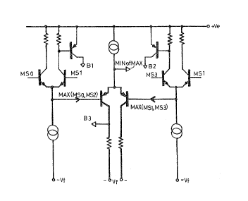
The invention relates to a method and an apparatus for accurate
digital determination of the time or phase position of a signal
pulse train in relation to a fixed time or frequency reference.
The arrangement generates and produces directly on the output a
digital word corresponding to the measuring value current at that
time.

The pulse train is compared in a plurality of EXCLUSIVE-OR gates
(OR0-OR3) with a number of reference clock signals (RCL0-RCL3)
which are mutually displaced in time. There is produced on the
output of each gate a signal (MS0-MS3) which is dependent on the
input signals of the gates with respect to frequency and pulse
ratio. The output signals from the gates are sent to a comparison
circuit (CO) in which a MIN of MAX operation is carried out, the
pulse ratio of the output signals (MSO-MS3) being compared and the
output signal which lies nearest to a predetermined pulse-ratio
value being subjected to analogue/digital conversion in a
converter (AD). The pulse train, in digital form, is thereafter
code-converted in a code converter (CC) together with the three
most significant bits taken from the pulse train prior to the
AD-conversion process. The thus produced binary code can be corrected
for systematic deviations resulting from frequency differences
between the frequency, reference frequency and/or sampling
frequency of the pulse train, by the addition/subtraction of a
predetermined numeric sequence.


French Abstract

L'invention est constituée par une méthode et un appareil servant à déterminer numériquement et avec précision l'instant où la phase d'un train d'impulsions par rapport à un instant ou à une fréquence fixe. Le dispositif de l'invention produit un mot numérique correspondant à la valeur mesurée à cet instant qu'il introduit dans le signal de sortie. Le train d'impulsion est comparé dans une pluralité de portes OU exclusif (OR0-OR3) avec des signaux d'horloge de référence (RCL0-RCL3) espacés les uns des autres dans le temps. € la sortie de chacune de ces portes est produit un signal (MSO-MS3) qui dépend de la fréquence et du rapport d'impulsion des signaux d'entrée des portes. Les signaux de sortie des portes sont transmis à un circuit de comparaison (CO) dans lequel une opération de détermination du minimum du maximum est effectuée, les rapport d'impulsions des signaux de sortie (MS0-MS3) étant comparés et le signal de sortie dont le rapport d'impulsion est le plus rapproché d'un rapport d'impulsions prédéterminé étant transmis à un convertisseur analogique-numérique. Sous forme numérique, le train d'impulsions est ensuite converti dans un convertisseur de code (CC) avec les trois bits les plus significatifs extraits du train avant la conversion analogique-numérique. Les déviations systématiques produites dans le code binaire ainsi créé qui sont dues aux différences entre la fréquence, la fréquence de référence et/ou la fréquence d'échantillonnage du train d'impulsions, peuvent corrigées par l'addition ou la soustraction d'une suite numérique prédéterminée.

Claims

Note: Claims are shown in the official language in which they were submitted.


The embodiments of the invention in which an exclusive
property or privilege is claimed are defined as follows:

1. A method for accurate digital determination of the
time or phase position of a signal pulse-train in a
telecommunication system, including the steps of:
forming a square-wave pulse-train from the signal
pulse-train;
comparing the square-wave pulse-train with a plurality of
mutually time-displaced square-wave reference signals to form
a plurality of new signals having mark/space ratios in
dependence on said comparisons;
mutually comparing the plurality of new signals in a MIN of
MAX operation to coarsely determine the time or phase
position of the signal pulse-train;
selecting the new signal whose mark/space ratio lies nearest
to a predetermined mark/space ratio;
converting the selected new signal to digital form; and
applying the coarsely determined time or phase position of
the signal pulse-train and the digitized selected new signal
to a code converter for producing a binary code value
representing the time or phase position of the signal
pulse-train;
wherein the binary code value can be corrected in respect of
systematic deviations resulting from frequency differences
among the pulse-train's frequency, the reference signals'
frequency and/or a sampling frequency of the pulse-train, by
addition/subtraction of a predetermined numerical sequence.


2. The method of claim 1, wherein the step of mutually
comparing the plurality of new signals in a MIN of MAX
operation includes the steps of low-pass filtering the
plurality of new signals and mutually comparing the low-pass
filtered new signals.

3. The method of claim 1 or 2, wherein the
predetermined mark/space ratio is 50:50, and the step of
selecting the new signal whose mark/space ratio lies nearest
to the predetermined mark/space ratio is based on the MIN of
MAX operation.

4. The method of claim 3, wherein the selecting step
includes the steps of applying low-pass filtered new signals
to a multiplexer and causing the multiplexer to select one of
the low-pass filtered new signals based on the coarsely
determined time or phase position of the signal pulse-train
produced by the MIN of MAX operation, and the selected new
signal is converted to digital form by applying the selected
new signal to an analog-to-digital converter.

5. An arrangement for accurately digitally determining
the time or phase position of a signal pulse-train in a
telecommunications system including:
a limiter for forming a square-wave pulse-train from the
signal pulse-train;
a plurality of EXCLUSIVE-OR gates, one input of each gate
receiving the square-wave pulse-train;


means for generating a plurality of reference clock signals,
a respective one of the reference clock signals being applied
to a second input of each of the gates, said reference clock
signals being displaced sequentially in time in relation to
one another, each of the gates producing an output signal
having a frequency and a mark/space ratio which is contingent
on the ratio between the signals on its first and second
inputs;
a multiplexor for selecting one of the output signals;
a comparison circuit in which a MIN of MAX operation is
carried out on the output signals, whereby the mark/space
ratios of the output signals are mutually compared and that
one of said output signals having a mark/space ratio value
which lies closest to a predetermined mark/space ratio value
is determined, that one output signal being selected by said
multiplexor and applied to an input of an analogue/digital
converter; and
a code converter, wherein the code converter receives on a
first number of inputs a signal from the analogue/digital
converter and on a second number of inputs a signal from the
comparison circuit, and the code converter converts the
signals on said first and second number of inputs to signals
in binary form which are produced on outputs of the converter
and which represent the time or phase position of the signal
pulse-train.

6. An arrangement according to claim 5, wherein the
signal from the comparison circuit constitutes the three most


significant bits of the time or phase position of the signal
pulse-train.

7. An arrangement according to claim 5 or 6, wherein
said predetermined mark/space ratio value is 50/50.


8. An arrangement according to claim 5, 6 or 7,
wherein the time-displacement between the reference clock
signals is 1/Nth of a clock period when the number of
reference clock signals is N.


9. An arrangement according to any one of claims 5 to
8, wherein the gates' output signals are connected to
corresponding inputs of a plurality of low-pass filters and
outputs from the filters are connected to the comparison
circuit and the multiplexor.


Description

Note: Descriptions are shown in the official language in which they were submitted.


~3~2:~
A MET}IOD AND AN ~RRANGEMENT FOR ACCUR~TE DIGI'I'~L DETERMININA~rloM
OF THE TIME OR PIIASE POSITION OF A SIGNAL PULSE TR~IN

TECHNICAL FIEI.D

The present invention relates to a method and an arrangement for
accurate digital determination of the time or phase position of a
signal pulse train relative to a fixed time or frequency referen-
ce. The arrangement is operative to generate a digital word which
corresponds to the measurement value which is current at that time
and produces said value directly on its output.

BACKGROUND ART

Two main methods for determining the time or phase position of a
signal pulse train are known to the art. These methods are known
respectively as the zero-crossing timing method and the complex
vector method.

When practising the zero-crossing method, the desired time
information is obtained by registering the position in a referen-
ce-divider chain at those moments when the pulse train changes
sign.

The time resolution obtained with this method is quite simply one
period of the highest reference frequency signal produc~d on the
input of the reference frequency-divider chain~ For example, in
order to determine the phase position oE a pulse train having a
repetition frequency of 1 MHZ with a resolution of 1 degree, it
would be necessary to apply a frequency of 360 MHZ to the input of
the frequency-divider chain. Consequently, the logic used to
determine the phase would need to be very fast, even in the case
of low-frequency pulse trains of moderate resolution.

Whenpractising the complexvectormethod, the information desired
is assumed to be included in the fundamental sine component of the
pulse train. This sine component is filtered-out and resolved into
two quadrature components, by correlation with sine and cosine

2~3~2 ~
reference-Erequencies in balanced mixers. Consequently, it i5 then
necessary to digitize the two results and to process the arc-
tangent of their ratio in a computer in order to determine the
phase.

DISCLOSURE OF THE INVENTION

The problem with the first of these methods is that it rec~uires the
use of highly advanced loyic, even when carrying out relatively
simple phase measurements.

The problem with the second method is that imperfections in the
10 analogue correlators introduce serious limitations into the method
in practice, and the need to process the arc-tan in a computer adds
greatly to the complexity oE the method.

The inventive arrangement is characterized by the inventive
features set forth in the claims and solves the aforesaid pro-
15 blems, by being operative to apply the pulse train to a pulseformer (limiter) which generates a square wave having a mark/-
space ratio of approximately 50/50. The square wave is applied to
N-number of EXCLUSXVE-OR circuits (e.g. 4) together with N-number
of reference-frequency signals in the form of square waves, which
20 signals differ in timing progressively by l/Nth of a cycle. The
requisite progressive time difference can be obtained, either by
commencing with a high fre~uency and dividing said frequency down,
or by utilizing delay lines. It is unimportant to the process
which of these methods is used. The mark/space ratio between the
25 N-output signals from the EXCLUSIVE-OR circuits are mutually
compared in comparison circuits in order to establish in which of
N-rough phase-sectors the signal phase lies. The signal which lies
nearest the pulse ratio 50/50 is then selected, filtered in a low-
pass filter and digitized in an analogue/digital converter to form
30 a binary code which provides finer phase information within the
rough sector that has already been determined. The advantages
afforded by the inventive arrangement over known techniques are
that time measurements or determinations can be made with an
accuracy greater than one period of the highest possible frequency


. ~ .

3 2 ~
ofthe reference clock, therewithenabling the operating frequency
ofthe arrangemerlt to be increased without requiring the provision
of very high-speed logic. Furthermore, i-t is not necessary for the
reference clock to be related precisely to the frequency of the
pulse train to be measured.

BRIEF DESCRIPTION OF THE DRAWINGS

The inventive arrangement will now be described in more detail
with reference to an exemplifying embodiment thereoE and with
reference to the accompanying drawings, in which
Figure 1 illustrates pulse-forming and time-displacement of the
signals;
Figure 2 illustrates how the pulse ratio (mark/space) varies on
the outputs of the EXCLUSIVE-OR circuits;
Figure 3 is a circuit diagram of an inventive comparison circuit;
and
Figure 4 is a block schematic of an inventive arrangement.

BEST MODE OF CARRYING OUT THE INVENTION

As evident from Figure 1, a pulse train WT in analogue form is
applied to the input of a limiter L. The limiter pulse-Eorms the
signal so as to produce on the output of the limiter a square wave
having the pulse ratio (mark/space) 50/50 ~ The square wave is
applied to a first input of each of N number of EXCLUSIVE-OR
gates, in the illustrated embodiment four gates. A reference clock
signal RCLO-RCL3 is applied to a second input of each of said
gates, said gates being referenced ORO-OR3. Each of these
reference-clock signals are square wave signals and are mutually
displaced in time and in sequence by l/N of a cycle. The output
signal from each EXCL~SIVE-OR gate is a square wave signal MSO-
MS3 having twice the frequency of the input-signal frequency of
respective gates and having a mark/space ratio depending on the
mutual clocking of the two input signals of the gates, as evident
from the diagram o~ Figure 2. The diagram shows variations in the
mark/space ratio for the output signals MSO-MS3 from the gates

s~ ~ 3 ~
ORO-OR3 as a function o e pUlSQ train clocking in rela-tion to
reference-clock-timing.

Efforts to derive the mutual clocking of the two input signals
from the outpu-t signal of one single EXCLUSIVE-OR gate will
introduce some element of doubt, sin~e it is impossible to ascer-
tain positively which 180 degree ranye contains the phase, but
this problem is solved by mutually c~mparing the output signals
~rom a plurality of EXCLUSIVE OR gates. For instance, when N e-
quals 4, in accordance with the illustrated embodiment, it is
possible to determine immediately within which 1/8th of the
reference-clock period the transitions of the input signal fall.
This is effected by comparison between the mark/space ratio of the
output signals of the gates ORO-OR3 in accordance with the
following MIN of MAX operation:
Table 1
If MSO > MS2 then let B1 = 0 else Bl = 1
If MS1 > MS3 then let B2 = 0 else B2 = 1
If MAX (MSO,MS2)> MAX (MSl,MS3) let B3 = O else B3=1.
Bl, B2 and B3 determine the three most significant bits in the
desired time measuring process subsequent to appropriate code
conversion from Gray to Binary form or some other output-signal
code.

The 3-bit word B1, B2, B3 now has a 1:1 agreement with the octant
within which the zero-crossing clocking of the signal lies

The aforesaid described Min of Max-operation can be implemented,
for instance, with the aid of a combination of NPN and PNP emitter-
followers, as illustrated in Figure 3, although it canl alterna-
tively, be realized with the aid of comparison circuits tcompara-
tors), switches and logic circuits. Figure 3 thus illustrates one
method o~ determining the three most significant bits of the
prevailing measurement value in accordance with Table 1.

In order to be able to determine the three least significant bits
LSB when measuring time, it is necessary to determine the mark/sp-
ace ratio of the signal on the output of at least one of the

20~3~ A
EXCLUSIVE-OR gates OR0-OR3 more accurately. In prac-tice, it is
beneficial to choose the gate whose mark/space ratio lies closest
to 50/50, since this pulse-form is less sensitive ko distortion as
a result of the restricted rise times of slow hardware logic. In
this case, the three most significant bits Bl, B2, B3 determined
in accordance with the aforegoing are used to select for finer an-
alysis the pulse which has this property. This is the pulse which
remains subsequent to the MIN of MAX operation.
i


As will be seen from Figure 4, this finer measurement of the
mark/space ratio can be effected with the aid of low~pass filters
LP0-LP3 for extraction of the mean value of the signal, followed
by analogue /digital conversion in an A/D-converter AD. In the
case of a high-speed application, a 4-bit A/D-converter of the
"FL~SH"-type can be used for instance. ~he inputs of respective
low~pass filters are connected to corresponding outputs of the
EXCLUSIVE-OR circuits OR0-OR3. The filter outputs are connected
to inputs of a comparison circuit CO and to the inputs of a
multiplexor M. The outputs from the comparison circuit, i.e. the
most significant bits Bl, B2 and B3, are applied to inputs on the
multiplexor M for the purpose of controlling the selection of that
gate output-signal (MS0-MS3) whose pulse ratio lies closest to
50/50. The most significant bits are also applied to inputs on a
code converter CC. The code converter is constructed either of
discrete logic gates or can be a look-up table in an ROM-memory.
The memory address consists of the three bits ~l,B2,B3 and the
bits (four or more) which constitute the result of said A/D-
conversion. The memory content consists of the desired output code
corresponding to each possible input bit-pattern. The output
signal from the multiplexor M is applied to the input of said A/D-
converter AD, the outputs of which are connected to correspondinginputs on said code converter CC, the outputs of which, in turn,
deliver binary coded signals. When a 4-bit A/D-converter is
combined, in this way, with the three most significant bits
Bl,B2,B3 an accuracy of 7 bits i5 obtained during the phase-
measuring process. Consequently, clocking, e.g., of a pulse trainwhose repetition frequency is 1 MHZ can be determined with a

2 0 3 ~ 'L
resolution of 1/128 ~s (8 ns) without needing to utili~e more than
1 MHZ reference clock-Erequency.

IE it is desired that a conventional binary code shall represent
the timing measurement, it is necessa;ry-to convert the three most
significant bits from the Gray code to binary code and to comple-
ment the three least significant bits LSB in alternating octants.
This can be effected with conventiona:L logic, tables or software.

Binary code-representation will facilitate correction of the
output value for any difference whatsoever between the reference
clock and the expected Erequency of the pulse train. Assume that
the expected nominal frequency of the pulse train is 1 000 003 HZ
but that the frequency of the available reference clocks is
precisely 1 000 000 HZ. Assume ~or the sake of simplicity that the
measuring accuracy is 7 bits and that 128 measurements are made
each second. The sequence of hinary values prior to correc-tion
will then have the following configuration for instance:
...... 59,62,65, ...... ,122,125,0,3,6,9,
which illustrates a stepwise increase of 3, modulo 128, depending
on said 3 HZ frequency difference. This can be corrected with the
aid of a 7-bit external memory whose content is increased with 3,
modulo 128, on each sampling occasion, this value being subtracted
from the measurement value prior to transmitting an output signal.

A similar technique can also be used when the relationship between
sampling period and reference-frequency deviation is more complex
and can, for instance, involve increasing the word length of the
memory with part quantities, or involve storing a full cycle of
correction values in the memory.

This shows that arithmetic configured in software or hardware
logic can be utilized for compensating non-integer relationships
between the midfrequency, reference clocks and measurement
frequency (sampling rate~ of the pulse train.


' :;

~. ~
2~3~
As will be evident from the aforegoing, the inventive arrangement
enables a significant improvement in measuring accuracy to be
achievedwithoutrequiring theprovision ofvery high-speed logic.


,
~ .

Representative Drawing
A single figure which represents the drawing illustrating the invention.
Administrative Status

For a clearer understanding of the status of the application/patent presented on this page, the site Disclaimer , as well as the definitions for Patent , Administrative Status , Maintenance Fee  and Payment History  should be consulted.

Administrative Status

Title Date
Forecasted Issue Date 1998-07-07
(86) PCT Filing Date 1990-03-28
(87) PCT Publication Date 1990-10-21
(85) National Entry 1990-11-22
Examination Requested 1992-11-24
(45) Issued 1998-07-07
Deemed Expired 2002-03-28

Abandonment History

There is no abandonment history.

Payment History

Fee Type Anniversary Year Due Date Amount Paid Paid Date
Application Fee $0.00 1990-11-22
Maintenance Fee - Application - New Act 2 1992-03-30 $100.00 1992-01-29
Registration of a document - section 124 $0.00 1992-02-14
Maintenance Fee - Application - New Act 3 1993-03-29 $100.00 1993-01-22
Maintenance Fee - Application - New Act 4 1994-03-28 $100.00 1994-02-04
Maintenance Fee - Application - New Act 5 1995-03-28 $150.00 1995-03-01
Maintenance Fee - Application - New Act 6 1996-03-28 $150.00 1996-02-26
Maintenance Fee - Application - New Act 7 1997-04-01 $150.00 1997-02-12
Final Fee $300.00 1998-03-23
Maintenance Fee - Application - New Act 8 1998-03-30 $150.00 1998-03-24
Maintenance Fee - Patent - New Act 9 1999-03-29 $150.00 1999-03-17
Maintenance Fee - Patent - New Act 10 2000-03-28 $200.00 2000-03-02
Owners on Record

Note: Records showing the ownership history in alphabetical order.

Current Owners on Record
TELEFONAKTIEBOLAGET LM ERICSSON
Past Owners on Record
DENT, PAUL WILKINSON
Past Owners that do not appear in the "Owners on Record" listing will appear in other documentation within the application.
Documents

To view selected files, please enter reCAPTCHA code :


To view images, click a link in the Document Description column. To download the documents, select one or more checkboxes in the first column and then click the "Download Selected in PDF format (Zip Archive)" or the "Download Selected as Single PDF" button.

List of published and non-published patent-specific documents on the CPD .

If you have any difficulty accessing content, you can call the Client Service Centre at 1-866-997-1936 or send them an e-mail at CIPO Client Service Centre.


Document
Description 
Date
(yyyy-mm-dd) 
Number of pages   Size of Image (KB) 
Drawings 1993-12-14 3 70
Abstract 1993-12-14 1 40
Cover Page 1998-07-06 2 90
Cover Page 1993-12-14 1 18
Claims 1993-12-14 2 100
Description 1993-12-14 7 322
Claims 1998-05-25 4 126
Claims 1997-07-30 4 126
Representative Drawing 1998-07-04 1 10
Correspondence 1998-03-23 1 37
International Preliminary Examination Report 1990-11-22 1 47
Prosecution Correspondence 1997-05-23 1 39
Examiner Requisition 1996-11-26 2 75
Prosecution Correspondence 1992-11-24 1 30
PCT Correspondence 1991-07-31 1 21
Office Letter 1992-12-09 1 29
Office Letter 1991-04-15 1 46
Fees 1997-02-12 1 68
Fees 1996-02-26 1 64
Fees 1995-03-01 1 78
Fees 1994-02-04 1 67
Fees 1993-01-22 1 44
Fees 1992-01-29 1 38