Language selection

Search

Patent 2030963 Summary

Third-party information liability

Some of the information on this Web page has been provided by external sources. The Government of Canada is not responsible for the accuracy, reliability or currency of the information supplied by external sources. Users wishing to rely upon this information should consult directly with the source of the information. Content provided by external sources is not subject to official languages, privacy and accessibility requirements.

Claims and Abstract availability

Any discrepancies in the text and image of the Claims and Abstract are due to differing posting times. Text of the Claims and Abstract are posted:

  • At the time the application is open to public inspection;
  • At the time of issue of the patent (grant).
(12) Patent: (11) CA 2030963
(54) English Title: ORTHOGONALLY POLARIZED DUAL-BAND PRINTED CIRCUIT ANTENNA EMPLOYING RADIATING ELEMENTS CAPACITIVELY COUPLED TO FEEDLINES
(54) French Title: ANTENNE A CIRCUIT IMPRIME FONCTIONNANT DANS DEUX BANDES A POLARISATIONS ORTHOGONALES ET UTILISANT DES ELEMENTS RAYONNANTS COUPLES CAPACITIVEMENT AUX LIGNES D'ALIMENTATION
Status: Expired
Bibliographic Data
(52) Canadian Patent Classification (CPC):
  • 351/56
  • 351/58
(51) International Patent Classification (IPC):
  • H01Q 13/08 (2006.01)
  • H01Q 5/00 (2006.01)
  • H01Q 21/06 (2006.01)
  • H01Q 21/26 (2006.01)
  • H01Q 25/00 (2006.01)
  • H03H 7/38 (2006.01)
(72) Inventors :
  • SORBELLO, ROBERT MICHAEL (United States of America)
  • ZAGHLOUL, AMIR IBRAHIM (United States of America)
(73) Owners :
  • COMMUNICATIONS SATELLITE CORPORATION (United States of America)
(71) Applicants :
(74) Agent: GOWLING LAFLEUR HENDERSON LLP
(74) Associate agent:
(45) Issued: 1995-08-15
(22) Filed Date: 1990-11-30
(41) Open to Public Inspection: 1991-06-15
Examination requested: 1990-11-30
Availability of licence: N/A
(25) Language of filing: English

Patent Cooperation Treaty (PCT): No

(30) Application Priority Data:
Application No. Country/Territory Date
450,770 United States of America 1989-12-14

Abstracts

English Abstract


A dual polarized printed circuit antenna operating in dual
frequency bands. A first array of radiating elements radiates
at a first frequency, and a second array of radiating elements
radiates at a second, different frequency. Separate power
divider arrays are provided for each array of radiating elements,
and the overall structure is provided in a stacked configuration.


Claims

Note: Claims are shown in the official language in which they were submitted.


7
WHAT IS CLAIMED IS:
1. In a dual polarized printed antenna comprising a ground
plane, a first power divider array disposed over said ground
plane, a first array of radiating elements disposed over said
power divider array, and second power divider array disposed over
said first array of radiating elements, and a second array of
radiating elements disposed over said second power divider array,
the improvement wherein said first array of radiating
elements comprises an array of radiating elements so configured
as to operate at a first frequency, and said second array of
radiating elements comprises an array of radiating elements so
configured as to operate at a second frequency that is different
from said first frequency.
2. An antenna as claimed in claim 1, wherein said second
frequency is lower than said first frequency.
3. An antenna as claimed in claim 2, wherein said first
and second power divider arrays comprise respective power divider
arrays for feeding said first and second arrays of radiating
elements at said first and second frequencies.
4. An antenna as claimed in claim 1, wherein elements in
said first array of radiating elements are smaller than elements
in said second array of radiating elements.
5. An antenna as claimed in claim 1, wherein said first
and second power divider arrays comprise tee junctions and
impedance transforming sections, the impedance transforming
sections of said second power divider array being longer than
the impedance transforming sections of said first power divider
array.


Description

Note: Descriptions are shown in the official language in which they were submitted.


2Q30963
~kl~ONALLy POLARIZED DUAL-BAND PR~NTED CIRCUIT
ANTENNA EMPLOYING RADIATING ELEMENTS
CAPACITIVELY COUPLED TO FEEDLINES


BACKGROUND OF L~ INVENTION
This invention relates to another improvement in a series
of inventions developed by the present inventors relating to
printed circuit antennas having their elements capacitively
coupled to each other, and in particular, two antennas wherein
the feed to the radiating elements is coupled capacitively,
rather than directly. The first in this series of inventions,
invented by one of the present inventors, resulted in U.S. Patent
No. 4,761,654. An improvement to the antenna disclosed in that
patent is described and claimed in U.S. Patent 5,005,019.

The antenna described in the foregoing U.S. patent and
patent application permitted either linear or circular polari-
zation to be achieved with a single feedline to the radiating
elements. The antennas disclosed included a single array of
radiating elements, and a single array of feedlines. One of the
improvements which the inventors developed was to provide a
structure whereby two layers of feedlines, and two layers of
radiating elements could be provided in a single antenna,
enabling orthogonally polarized signals to be generated, without
interference between the two arrays. U.S. Patent 4,929,959
discloses and claims such a structure.


~.


2030963


Having developed the dual-band orthogonally
polarized antenna, various experiments have been
conducted with different shapes of radiating elements,
and antenna configurations. Commonly assigned U.S.
Patent 4,926,189 is directed to such an array employing
gridded antenna elements.
The work on dual polarized printed antennas
resulted in the provision of an array which could
operate in two senses of polarization, a lower array of
the antenna being able basically to "see through" the
upper array. The improvement represented by the
present invention is to extend that concept.

SUMMARY OF THE INVENTION
IN view of the foregoing, it is one object of the
present invention to provide a high-performance, light
weight, low-cost dual-band planar array. The inventors
have determined that employing certain types of antenna
elements for the upper and lower arrays enables
operation at two different, distinct frequency bands
from a single radiating array structure.


B

2030963


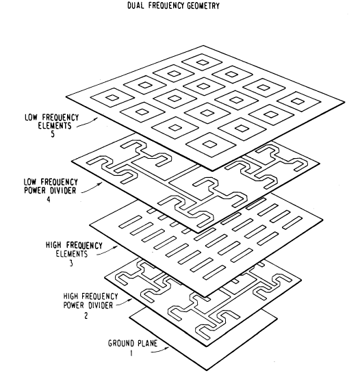
BRIEF DESCRIPTION OF THE DRAWINGS
Figure 1 shows an exploded view of the dual frequency
antenna of the invention; and
Figures 2-8 show graphs of the measured performance of a
sixteen-element dual band array.


DETAILED DESCRIPTION OF THE PREFERRED EMBODIMENT
Referring to Figure 1, the inventive structure, as described
also in U.S. Patent No. 4,929,959,
comprises five layers. The first layer is a ground plane 1. The
second layer is a high frequency power divider 2, with the
individual power divider elements disposed at a first
orientation. The next layer is an array of high frequency
radiating elements 3. These three layers together define the
first operating band array Bl, in which layers 1 and 3 form the
ground plane for the power divider 2.
The operating frequency of the array is dictated by the
dimensions of the radiating elements and the power distribution
network. The array of high frequency elements 3 will have
physically smaller radiating slots than those used in the low
frequency array. The principal controlling factor in the
resonant frequency of the slot is the outer dimension (radius
or ~ide) of the element. This dimension is inversely propor-
tional to the operating frequency. As a rule of thumb, for a
circularly-shaped element, the diameter i8 approximately one-
half of the operating wavelength; for a square or rectangularly-
shaped element, a side (longer side for a rectangle) is

approximately one-half the operating wavelength. Those of


~ ,
~'

2030963

working skill in this field will appreciate that the actual
dimension~ may vary somewhat, according to the earlier-stated
pre~criptions.
The power divider 2 may consist of impedance transforming
sections at the tee junctions where the power split is performed.
These transforming sections typically are ~/4 in length, where
~ refers to the wavelength at the operating frequency. The

transformer length also will be inversely proportional to the
operating frequency.
Disposed above the high frequency elements 3 is a low
frequency power divider array 4, with the individual power
divider elements disposed orthogonally with respect to the
elements of the power divider 2. Above the low frequency power
divider 4 is a second array of radiating elements 5, these
elements 5 being low frequency radiating elements. The layers
3-5 together form a second operating band array B2, wherein the
layers 3 and 5 provide the ground plane for the power divider 4.
The element designs in layers 3 and 5 are designed appropriately
to minimize both radiation interaction between the lower and
upper arrays, and coupling between the two power distribution
networks.
As discussed previously, the physical size of the elements
in the layer 5 will determine the operating frequency. The
elements of the low frequency array 5 will be larger than those
of the high frequency array 3. Transformer sections within the
low-frequency power divider network will be longer than those
used in the high frequency divider, but otherwise the divider
networks may be very similar in design.


2030963_
All of the layers 1-5 may be separated by any suitable
dielectricl preferably air, for example by providing ~Nomex
honeycomb between the layers.
The structure depicted in Figure 1 shows the design and
construction for a dual-band linearly polarized flat-plate array.
Linear polarization is dictated by the radiating elements.
Circular polarization may be generated by choosing the
appropriate e~ements with perturbation segments as described, for
example in U.S. Patent No. 5,005,019. U.S. Patent No. 4,929,959
also shows examples of such elements.
The measured performance of a 16-element dual band linear
array is depicted in Figures 2-8. For one sense of polariza-
tion, the band of interest is 11.7-12.2 GHz, and for the other,
orthogonal sense of polarization, the band of interest is 14.0-
14.5 GHz. Figure 2 shows the input return loss for both senses
of polarization (in each instance, the input match is very good
over a broad band, as can be seen from the figure). Figure 3
shows the corresponding radiation gain for each polarization.
As shown in the Figure, both senses of polarization radiate very
efficiently and over a broad band, and the radiation efficiency
of each i8 comparable.
Figure 4 shows the port-to-port or array network isolation.
The i~olation is sufficiently high to ensure that the two arrays
are virtually decoupled, and operate as required in an
independent manner. Figures 5-8 show a corresponding on axis
swept cross polarization and radiation patterns for each
frequency band, demonstrating the efficiency of the radiatinq
array, and the low radiated cross polarization.


* Trademark


~,.,. 1 .

2030963


While the invention has been described with reference to a
particular preferred embodiment, various modifications within the
spirit and scope of the invention will be apparent to those of
working skill in this technical field. For example, although the
foregoing measured data shown in the figures was provided with
respect to specific frequency bands, the invention represents a
design that can be implemented for any two distinct frequency
bands, and for any size array or any number of elements. Thus,
the invention should be considered limited only by the scope of
the appended claims.


Representative Drawing
A single figure which represents the drawing illustrating the invention.
Administrative Status

For a clearer understanding of the status of the application/patent presented on this page, the site Disclaimer , as well as the definitions for Patent , Administrative Status , Maintenance Fee  and Payment History  should be consulted.

Administrative Status

Title Date
Forecasted Issue Date 1995-08-15
(22) Filed 1990-11-30
Examination Requested 1990-11-30
(41) Open to Public Inspection 1991-06-15
(45) Issued 1995-08-15
Expired 2010-11-30

Abandonment History

There is no abandonment history.

Payment History

Fee Type Anniversary Year Due Date Amount Paid Paid Date
Application Fee $0.00 1990-11-30
Registration of a document - section 124 $0.00 1991-10-23
Maintenance Fee - Application - New Act 2 1992-11-30 $100.00 1992-11-16
Maintenance Fee - Application - New Act 3 1993-11-30 $100.00 1993-11-16
Maintenance Fee - Application - New Act 4 1994-11-30 $100.00 1994-11-22
Maintenance Fee - Patent - New Act 5 1995-11-30 $150.00 1995-10-12
Maintenance Fee - Patent - New Act 6 1996-12-02 $150.00 1996-10-22
Maintenance Fee - Patent - New Act 7 1997-12-01 $150.00 1997-11-12
Maintenance Fee - Patent - New Act 8 1998-11-30 $150.00 1998-11-18
Maintenance Fee - Patent - New Act 9 1999-11-30 $350.00 2000-01-04
Maintenance Fee - Patent - New Act 10 2000-11-30 $200.00 2000-11-20
Maintenance Fee - Patent - New Act 11 2001-11-30 $200.00 2001-11-20
Maintenance Fee - Patent - New Act 12 2002-12-02 $200.00 2002-10-31
Maintenance Fee - Patent - New Act 13 2003-12-01 $200.00 2003-11-03
Maintenance Fee - Patent - New Act 14 2004-11-30 $250.00 2004-11-04
Maintenance Fee - Patent - New Act 15 2005-11-30 $450.00 2005-11-02
Maintenance Fee - Patent - New Act 16 2006-11-30 $450.00 2006-10-30
Maintenance Fee - Patent - New Act 17 2007-11-30 $450.00 2007-10-30
Maintenance Fee - Patent - New Act 18 2008-12-01 $450.00 2008-10-30
Maintenance Fee - Patent - New Act 19 2009-11-30 $450.00 2009-10-30
Owners on Record

Note: Records showing the ownership history in alphabetical order.

Current Owners on Record
COMMUNICATIONS SATELLITE CORPORATION
Past Owners on Record
SORBELLO, ROBERT MICHAEL
ZAGHLOUL, AMIR IBRAHIM
Past Owners that do not appear in the "Owners on Record" listing will appear in other documentation within the application.
Documents

To view selected files, please enter reCAPTCHA code :


To view images, click a link in the Document Description column. To download the documents, select one or more checkboxes in the first column and then click the "Download Selected in PDF format (Zip Archive)" or the "Download Selected as Single PDF" button.

List of published and non-published patent-specific documents on the CPD .

If you have any difficulty accessing content, you can call the Client Service Centre at 1-866-997-1936 or send them an e-mail at CIPO Client Service Centre.


Document
Description 
Date
(yyyy-mm-dd) 
Number of pages   Size of Image (KB) 
Cover Page 1995-08-15 1 20
Abstract 1995-08-15 1 12
Description 1995-08-15 6 196
Claims 1995-08-15 1 40
Drawings 1995-08-15 8 169
Representative Drawing 1999-07-19 1 32
Prosecution Correspondence 1990-11-30 1 30
Prosecution Correspondence 1994-10-27 1 31
Prosecution Correspondence 1994-09-22 3 77
Examiner Requisition 1994-06-23 2 81
PCT Correspondence 1994-10-14 4 137
Office Letter 1991-04-18 1 47
Office Letter 1991-05-02 1 24
PCT Correspondence 1995-06-07 1 42
Office Letter 1994-10-25 1 36
Fees 1992-11-16 1 32
Fees 1996-10-22 1 49
Fees 1995-10-12 1 38
Fees 1993-11-16 1 34
Fees 1994-11-22 1 42