Note: Descriptions are shown in the official language in which they were submitted.
2~31~5~1
1 -
INVERSE MULTIPLEXER AND DEMULTIPLEXER TECHNIQUES
Technical Field
The present invention relates to inverse multiplexer techniques that
demultiplex high non-standard channel data rate signals and adapt each non-standard
5 data rate signal to lower standard channel data signals for tr~n~mi.csion over a
commercial co~ ication network to a remote receiver where an inverse
demultiplexer adapts and multiplexes the received standard data rate signals to
reproduce the original non-standard higher data rate signal and transmit it to the
destined user.
10 Description of the Prior Art
In recent years there is a substantial need for comm~lnicating with data
rates between lO Mb/s to I Gb/s, as, for example, the SONET STSI' 51.84 Mb/s
and SONET STS3~ 155.52 Mb/s tr~n~mi.csion rates, High Definition Television
programming at 120 Mb/s or greater, and a Gb/sec supercomputer tr~ncmission rate.
15 Such applications cannot directly transmit data messages over existing
telecommllnic~tions networks using, for example, the 45 Mb/s DS3 rate, because the
data rate of the specialized application does not match, and may be greater than the
data rate used by the existing telecomm~lni~ation netu~orks. Therefore, to transmit
data messages for such applications between remote locations, it becomes necessary
20 to build a separate, specially designed, telecommunication network to link these
remote locations. Where such remote locations are spread over wide distances, such
as across the United States, the development costs may not justify construction of
short or long haul facilities to support each of the different specialized applications.
An alternative solution might be to design specialized data rate
25 converters to meet the criteria of each application. In this regard see, for example,
U. S. Patent 4,322,844 issued to F. Fellinger et al. on March 30, 1982, where a
tr~nsmitter-receiver synchronizer provides bidirectional rate conversion betweenframes of data having a first rate and a first format, and frames of data having a
second rate and a second format. In such synchronizer, a first frame of data at a first
30 rate, and a second frame of data at a second rate are stored in a separate first and
second buffer memory, respectively, during a first frame interval, and each frame of
data is read out at the other rate during a second frame interval. Additionally, during
the second frame interval, a third frame of data at the second rate, and a fourth frame
of data at the first rate are read into the first and second buffer memories,
35 respectively, and read out at the other rate during a third frame interval, etc. Another
synchronizer is shown in U. S. patent 4,558,445 issued to L. R. Novick on
*Trade Mark
. ~ .
2031054
D~ce~ ~r 10, 1985, wherein an applique rate converter generates a composite datastream comprising ~ltern~te data bits and data boundary bits, and the synchronizer
increases such composite stream to the output data rate. Such specialized
arrangements are expensive and would require a new design for converting different
5 data rates associated with each different application, and may not be usable for all
applications.
Therefore, the problem remaining in the prior art is to provide a
technique that permits specialized applications to economically send their higher
data rate signal over existing lower data rate telecom,llullication networks, and
10 thereby avoid constructing expensive specialized high data rate long or short haul
nt;lwolks, or expensive specialized data rate converters, and provide for a moreeconomic use of the unused capacity of existing networks.
Summary of the Invention
The foregoing problem in the prior art has been solved in accordance
15 with the present invention which relates to Inverse Multiplexer and Inverse
Demultiplexer techniques. An Inverse Multiplexer includes a Delmlltirlexer whichdemnltirlexes a high data rate input signal to subsectional output signals whichcomprise fractional parts of that high data rate signal, and synchronization means
which marks each of the subsectional output signals for later resynchronization at the
20 receiver. A Prog,~ ,able Multiplexer then multiplexes one or more of such
subsectional output rate signals for tran~mi~sion over existing facilities.
Other and further aspects of the present invention will become appalent
during the course of the following description and by reference to the accompanying
drawings.
25 Brief Description of the Drawin~s
FIG. 1 is a block diagram of an exemplary arrangement of a
con "~ ic~tion system for practicing the present invention;
FIG. 2 is an illustration of the preferred rate-adaptation technique which
maps a capacity domain frame into a time domain frame for an exemplary input
30 signal to a Programmable Multiplexer in the arrangement of FIG. 1 using a two-step
method in accordance with the present invention;
FIG. 3 is a table listing the conversion of the capacity domain to time
domain assignments for use in the mapping of FIG. 2 for the exemplary two-step
method in accordance with the present invention;
20310~4
FIG. 4 is a block diagram of an exemplary programmable multiplexer in
accordance with the present invention; and
FIG. 5 is a block diagram of an alternative programmable multiplexer in
accordance with the present invention.
FIGS. 6 and 7 are block diagrams of a preferred embodiment of the
synchronization and resynchronization means of FIG. 1.
Detailed Description
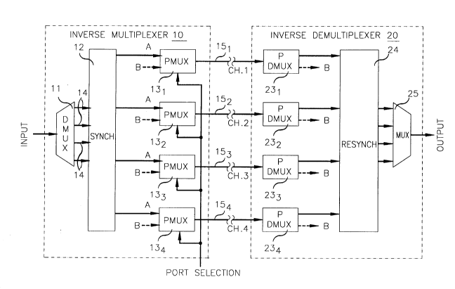
FIG. 1 illustrates an exemplary arrangement for each of an Inverse
Multiplexer 10 and a remote Inverse Demultiplexer 20 which are interconnected to10 form an exemplary co~ unication system in accordance with the present invention.
For purposes of explanation only, and not for purposes of limit~tion, the following
description of the present invention will be directed to (1) an exemplary Inverse
Multiplexer 10 which receives an exemplary SONET ST3 155.52 Mb/s tr~nsmiccion
rate input signal, and transmits such input signal over four exemplary DS3 45 Mb/s
15 rate ch~nnels 151 to 154 of a conventional co~ tion system to (2) an
exemplary remote Inverse Demultiplexer 20 for receiving the exemplary four DS3
ch~nnel signals and reconstructing the exemplary original SONET ST3 signal
the~crlo~. It is to be understood that the input signal can comprise any data rate
other than the SONET ST3 signal which is greater than the data rate of the
20 co--...."-~ic~tion channels 15 used by the co--".~ ication system for tr~ncmicci~n
between remote locations.
In FIG 1. the exemplary Inverse Multiplexer 10 is shown as comprising
a Demultiplexer 11, a synchlol-;7i~t;on means 12, and a plurality of N-~ Rate
Adaptation means which can comprise any suitable means, but hereinafter will be
25 dçsrribed in rel~tionchip to Prog~d~ able Multiplexers (PMUXs) 131 to 134. Inoperation, Demultiplexer 11 receives the exemplary SONET ST3 155.52 Mb/s data
rate input signal, and demultiplexes the input signal into a plurality of subsectional
output signals, where each subsectional output signal includes a data rate which is
less than the exemplary standard 45 Mb/s DS3 channel 15 tr~nsmi~sion data rate.
30 Such dem-lltiplexing should produce subsectional output signals with data rates that
(1) are fractional parts of the input data rate, and (2) are less than the data rate of the
co....~ -ication system channels 15. It is to be understood that each subsectional
output signal should have a data rate less than the communication system channel 15
data rate, but need not have a data rate which equals the data rate of any of the other
35 subsectional output signals. For purposes of explanation only, however, it will be
~cs~lm~d that demllltiplexer 11 produces four subsectional output signals having
2031054
equal data rates of 38.88 Mb/s each, which is less than the 45 Mb/s exemplary DS3
ch~nnel 15 tr~n~mi~;on data rate.
It is to be understood that demultiplexer 11 could have produced any
number of subsectional output signals above 4 with equal or unequal data rates, as
5 long as each of the subsectional output signals had a data rate which is less than the
channel 15 tr~n~mi~ion data rate of the co.. ~ is~tiQn system being used. For the
above example, at least 4 subsectional output signals are required for the present
exemplary 155.52 Mb/s rate input signal, since any lesser number would produce at
least one subsectional output signal with a data rate higher than the exemplary 45
10 Mb/s r~nnel 15 data rate. Each of these demultiplexer 11 subsectional output
signals are tr~nsmitted over separate paths 14, or other means, e.g., ch~nnel~, to a
synchronizing means 12.
Synchronizing means 12 can comprise a separate synchronizer for each
subsectional output signal from demultiplexer 11, as shown in FIG. 6 for a ~ f~ d
15 embo~liment of synchronizing means 12. In FIG. 6, an exemplary arrangement for a
synchronizer 124, in the tr~nsmitting end, is shown as compri~ing an elastic store 40,
a marker insert circuit 41 and a phase lock loop comprising a low pass filter 42 and a
Voltage Control Oscill~tor (VCO) 43. In operation, a clock at the input data rate
(e.g., 155.52 Mb/s) is received in Inverse multiplexer 10 and divided by N (e.g.,
20 N=4) to produce the subsectional clock signal at the data rate of the input
subsectional output signal (e.g., 38.88 Mb/s) from dçmlllsiplexer 11. The
subsectional clock signal is provided to each of the synchronizers 121 to 124, but, for
oses of simplicity, only one of the synchronizers is shown as receiving this
clock signal, which for the present example of FIG. 6 is synchronizer 124. In the
25 synchronizer 12i elastic store 40 receives the subsectional output data and clock
signals and places gaps in the data stream to permit Ill~kel s to be inserted atpredete~ ed intervals. Marker insert 41 receives both the data from the elastic
store 40 and the clock signal from the output of the phase lock loop comprising low
pass filter 42 and VCO 43, and periodically inserts a marker signal into the
30 subsectional output data stream from elastic store 40. Marker insert 41 also provides
a clock signal, associated with the clock from the phase lock loop, to elastic store 40,
and a synchronizing pulse externally to each of the other synchronizers 121 to 123, if
synchronizer 124 is the master synchronizer. Each of the other synchronizers 121 to
123 use such synchronization pulse from marker insert 41 of synchronizer 124 along
35 with the input clock signal provided by phase lock loop 42, 43 as shown as part of
synchronizer 124. The data and clock signals from marker insert 41 are then sent to
20~1054
the associated PMUX 13j. Therefore, each synchronizer inserts a synchronization
marker into each subsectional output signal from DMUX l l in response to a
synchronization pulse, and passes the synchronized subsectional output signal to the
5 associated PMUX 13j. For purposes of explanation hereinafter, it will be assumed
that the 38.88 Mb/s subsectional output signal from DMUX 11 was increased to
39.00 Mb/s at the output of each synchronizer 12 by the inclusion of the associated
marker signal in each synchronizer 12j.
Each of the four synchronized data rate subsectional output signals
10 from synchronizing means 12 is provided to the input of a separate one of PMUXs
13, to 134. Since each of the PMUX of the exemplary arrangement of FIG. l are
shown as receiving a single input signal at a data rate of 39 Mb/s at Data Port A
and no signal at Data Port B, the following description of PMUX 13, also applies to each of PMUXs 132 to 134. It should be understood, however, that any Inverse
15 Multiplexer should include two functions; tributary synchronization and rate
adaptation. Tributary synchronization is required to automatically compensate for
difference in the DS3 path lengths of channels 15 due to differences in circuit
packs, cross-connect cables, and wires or optical fibers. The problem can be
solved by inserting synchronized digital markers into each of the paths or channels
2 o 15 at the transmit end and then using that marker information to realign the frames
at the receiving end. The delay required by the realignment process can be
provided by large elastic stores.
The second function of rate adaptation will always be required since
the input data rate will almost never be a convenient multiple of the exemplary
25 DS3 channel rate. A solution is to insert data from another source into fixedpositions within the exemplary DS3 frame to stuff the incoming data up to the
exemplary DS3 rate. Such synchronization process is described in U.S. Patent
5,062,105 assigned to the same assignee. The arrangement of FIG. 1 only shows a
single active input at Data Port A to each of PMUXs 13, but the insertion of data
3 o from another source at Data Port B, etc., is shown in the above-mentioned patent to
R.R. McKnight et al. Such arrangement will be described briefly once the
operation of PMUX 13l with a single input has been described.
PMUX 13, receives the exemplary synchronized 39 Mb/s subsectional
input signal and inserts such signal up into the 45 Mb/s DS3 frame so that the signal is
35 substantially evenly distributed over the DS3 frame by mapping the input
- 20310~4
- 6 -
re~lui~ ~nls in the capacity domain into a time domain. As described in detail in
the above-men~ione~ copending patent application to R. R. McKnight et al., a
PMUX can accomplish this via a 2-step or 3-step digit reversal technique. For
purposes of explanation only, the following description is directed to the 2-step digit
S reversal technique. The funcl~m~ntal goal of the digit reversal technique is to
provide a mapping from a capacity domain to a time domain.
FIG. 2 illustrates an example of the mapping of the capacity domain to
the time domain for the 2-step digit reversal technique for a PMUX 131 comprising
only the 39 Mb/s subsectional output signal at input data port A. For purposes of
10 description, it will be ~sumed that the capacity domain includes a capacity frame 30
of forty-five sequential capacity domain time slots (CTSs 00-44) with each Capacity
domain Time Slot represçnting and exemplary 1 Mb/s of capacity. For the present
eY~mple, data port A receives a subsectional output signal with a 39 Mb/s data rate
from synchronization means 12. Since only an integral number of Capacity Time
15 Slots (CTS) can be assigned to a data port, data port A will be ~igne~l 39 CTSs in a
contiguous segment of the capacity domain frame. An optional asynchronous pulse
stuffing algorithm 72 of FIG. 4 can be used to fill in any fraction of a CTS which is
not needed for the subsectional output signal. As shown in FIG. 2 for the capacity
domain frame 30, data port A is arbitrarily assigned CTSs 00-38 to accommodate the
20 39.00 Mb/s capacity requirement. It is to be understood that data ports A could have
been assigned any portion of the 00-44 CTSs of the capacity domain frame 30 which
does not overlap other data port (e.g., Data Port B) requirements.
In accordance with a first step of the present digit reversal technique, the
capacity domain CTS address is decomposed as a predetermined number of digits
25 (e.g., 3 digits for the 00-44 CTS) from a set of number bases. More particularly, to
determine the number bases to be used, any combination of numbers that, when
multiplied together, will provide the number of CTSs of the capacity domain frame
30 can be used. For example, for the 45 CTSs of the capacity domain frame 30,
combinations such a 9 and 5; 3 and 15; and 3, 3, and 5 when multiplied together will
30 yield a value of 45. Although any of these combinations may be used for the
following calculations, the following example will use the number bases 3, 3 and 5
since it provides a clearer example of the method. Typically, using a combination
with more numbers, e.g. 3, 3 and 5 rather than just 5 and 9, will provide a somewhat
more even distribution of the CTSs amongst the Time Domain Time Slots (TDTS) in
35 Time Capacity frame 31. However, factors of 3 are best combined with other factors
rather than separate, to obtain uniformity of distribution. Therefore, for the number
20310S4
- 7 -
systems of 3, 3, and 5 to be used, the available range of numbers would be 0-2, 0-2
and 0-4, respectively, as is well known in the art. In decomposing the capacity
domain CTS numbers for the exemplary number systems chosen, the first step of the
present digit reverse technique uses the equation:
S X=Xl-3-5+X2-5+X3 (1)
where X is the CTS address, and Xl to X3 are integers which would be substituted to
produce the CTS address X.
FIG. 3 shows a Table which illustrates the various values of Xl to X3
which need to be multiplied with the associated data base numbers in Equation (1) to
10 produce each of the CTS addresses. For example, for the CTS address where X=00
in capacity domain frame 30 of FIG.2, representative of the first CTS of data port A,
Xl to X3 would have to equal zero in equation (1) to yield X=00. Similarly, for CTS
address X=38 in frame 30 of FIG. 2, representative of the last CTS for data port A,
Xl would have to equal 2, X2 would have to equal 1, and X3 would have to equal 3in equation (1) to yield 30+5+3=38.
Having completed the above first step for each of the used CTSs in
capacity domain frame 30, the second step is to generate a digit reverse technique by
reversing (1) the number base sequence, and (2) the Xi values, and generate the
following equation in the same manner as used for generating equation (1):
Y=X3 3 3+X2 3+Xl (2)
where Y is the assigned le~ senlalive time slot in a exemplary DS3 Time Domain
frame 31, comp~ising 45 time slots, for the CTS of Capacity Domain frame 30 of
FIG. 2. For example, for CTS 05 of Capacity Domain 30 assigned to data port A, in
accordance with the Table of FIG. 2, Xl and X3 of equation (1) would equal 0 while
25 X2 would equal 1 to produce X=05. Substituting these Xi values into equation (2)
would produce Y=03 representative of time slot 03 of time domain frame 31.
Therefore, the data in CTS 05 in frame 30 would be tr~ncmitted over channel 15l of
FM. 1 as data in time slot 03 of Time Domain frame 31 using this 2-step digit
reverse technique. Similarly, as seen from the Table of FIG. 2, the data assigned to
30 CTSs 08 and 23 would be tr~ncmitte~l over channel 151 in time slots 30 and 31,
respectively, of time domain frame 31. In this manner the contiguously assigned
capacity domain time slots in frame 30 for data port A are distributed somewhat
..
203105~
uniformly through time domain frame 31, as are the unused CTSs for CTSs 39-44,
which are stuffed.
An alternative 3-step digit reverse technique can be used to provide a
more even distribution of the CTSs of capacity domain frame 30 In this 3-step digit
5 reverse technique the first step of the above-described 2-step technique usingequation (1) is repeated as the first step of the 3-step digit reverse technique. A
second step of the 3-step digit reverse technique involves the conversion of thedetermined values of Xl to X3 into equivalent Yl to Y3 values, respectively, using
mod~ r ~rithmetie as described in the copending patent application to R.R.
10 McKnight et al. The third step of the 3-step digit reverse technique uses the equation
Y=Y3 3 3+Y2 3+Yl (3)
which is derived in the same manner as equation (2) but sub~liLules the Yi for the Xi
values of equation (2). It is to be understood that the advantage of the present 2-step
and 3-step techniques are that the time slots are substantially uniformly distributed
15 within a time domain frame and that all capacity domain CTSs are guaranteed to be
mapped inside time domain frame 31.
Exemplary arrangements for programmable multiplexer 131 for
pclrc~lllfing the above 2-step or 3-step techniques are shown in FIGs. 4 and 5. In
FIG. 4 a frame counter 60 receives a clock signal which is passed through a plurality
20 of dividing circuits 61-63 that provide binary value outputs relating to the time slot
numbers in time domain frames 31 in FIG. 2. For purposes of explanation, the
following description of the PMUX of FIG. 4 will be related to the prior example of
a capacity and time domain frame of 45 CTSs, where the number bases 3, 3 and 5 are
used. Therefore, frame counter 60 would include a divide-by-3 circuit 61, a divide-
25 by-3 circuit 62, and a divide-by-5 circuit 63. Since the binary output from the
divide-by-3 circuits 61 and 62 can only be a binary "0", "1", or "2", there will be two
output leads from each divide-by-3 circuit, while the divide-by-5 circuit 63 provides
3 output leads to take care of the possible 000, 001, 010, 011 and 100 binary codes.
The first output lead from divide-by-3 circuit 61 will be considered as the Least
30 Significant Bit (LSB) while the highest value binary output lead from divide-by-5
circuit 63 is considered the Most Significant Bit (MSB). It should be noted that the
LSB-MSB bits from frame counter 60 are coupled to comparators 67 and 68
associated with Data Port A, in a reverse order, as shown by the exemplary dashed
line for the LSB from divide-by-3 circuit 61 to the MSB input for comparator 67 of
- 20310~4
Data Port A, to automatically produce the digit reversal technique.
Each input data port termin~te~l as an input to a PMUX 13, is provided
with a Start Bit Memory 65 and an End Bit Memory 66 which are coupled to a firstassociated Comparator 67 and a second associated Comparator 68, respectively.
5 These memories and Comparators are effectively associated with the Capacity
Domain frame 30 of FIG. 2. Each of first and second Comparators receives the bits
on the 7 output leads from frame counter 60 in the reverse order at separate inputs
thereof. The outputs from each of the first and second Con~a ato~s 67 and 68,
associated with input Data port A, are connected to separate inputs of a separate
10 associated AND gate 69, and the output from AND gate 69 is connected to a first
input of a separate second AND gate 70. The data signal from a synchlonizer 12i
associated with that input Data Port is applied to the second input of the associated
AND gate 70. The outputs from the second AND gate 70 is shown as coupled to an
input of an optional OR gate 71, with the output of OR gate 71 being applied to
15 channel 151 for tr~n~mi~sion to the far-end Inverse Demultiplexer 20.
In operation, a control signal ini~i~li7es the Start Bit memory 65 and
End Bit memory 66 for each of the input data ports, which for the present example is
only Data Port A. In the present example shown in F~G. 2, the start and end bit
m~m~rieS 65 and 66 for Data Port A would be set at 00 and 38, respectively, since
20 those are the arbitrarily assigned contiguous CTSs in capacity domain frame 30 for
- Data Port A. Similarly, the Start and End Bit memories 65B and 66B for any other
Data Port that could be connected to the input of PMUX 131 would be set at 39 and
40-44, respectively, depending on the amount of capacity domain required, but could
not be more than the unassigned 6 CTSs.
In the present example, when frame counter 60 provides binary signals
on its 7 output leads inclic~ing the address of a particular Time Domain Time slot,
each of first comparators 67 co~ ales the associated stored Start Bit value with the
bit reverse binary value from frame counter 60 and outputs a binary " 1" if the
reversed binary value from frame counter 60 is equal to or greater than the associated
30 Start Bit value, and a "0" if the reversed binary value from frame counter 60 is less
than the stored Start Bit. Similarly, each of second comparators 68 colllpal~s the
associated stored End Bit value with the reversed binary values from frame counter
60 and outputs a binary " 1 " if the associated End Bit value is equal to or less than the
received reversed binary value from frame counter 60, and a binary "0" if the
35 associated End Bit value is greater than the reversed binary value received from
frame counter 60.
- 203105~ -
- 10-
Therefore, for the period of time of time domain time slot number
Y=12, frame counter 60 would output the equivalent binary value for 1,1,0 for X3 to
Xl, respectively, as shown in the table of FIG. 3. Each of comparators 67 and 68 for
Data Ports A (and B) would receive the reverse value of 0,1,1 (X=06) from frame
5 counter 60, because of the lead reversal between frame counter 60. Comparators 67
then compare the stored Start Bit value of associated memory 65 with the received
reverse binary code. Only comparator 67 for Data Port A would output a binary "1"
since this comparator would find it equal to or greater than the stored Start Bit value
of 00 in associated Start Bit memory 65. Comparators 67 for any other Data Port
10 would determine that the received reverse binary code is less than the stored Start Bit
value and output a binary "0". However, for comparators 68 of Data Port A, and
Data Port B, each comparator 68 would output a binary " 1 " since the received binary
code 0,1,1 (equal to digit X=6) is less than the End Bit value stored in each of End
Bit m-omories 66.
As a result, only AND gate 69 associated with Data Port A would
produce a binary "1" enable output signal during time domain frame time slot Y=12
because both of its inputs from comparators 67 and 68 equal a binary "1 ". This
enable output signal from AND gate 69 of Data Port A provides a binary "1" enable
signal to AND gate 70 to permit the input data signal from Data Port A to pass
20 th~ hlough, and to optional OR gate 71, for tran~mission over channel 151. A
similar process occurs for each of the time domain time slots Y=00-38 in the Table
of FIG. 3 to permit Data Port A to be ~ccesse~l in accordance with the capacity
domain during each of the Time Domain Time Slots. If Data Port B were included,
then the associated comparators 67B and 68B and AND gates 69B and 70B would
25 operate to permit Data Port B to be accessed in accordance with the capacity domain
CTSs 39 and up during each of the time domain time slots.
To permit the 3-step technique to be performed, an optional converter 73
need only be disposed at the output of frame counter 60 to perform the conversion
for the number base values from Xl to X3 to Yl to Y3, respectively, using modular
30 alithllRtic as described in copending patent Application to R. R. McKnight et al.
These converted Yl to Y3 values are then used in equation (2) for Xl to X3,
respectively. FIG. 5 illustrates an exemplary alternative preferred arrangement for
pelrc,lll~ing the 2-step or 3-step digit reverse technique, in which the capacity domain
parameters are provided to a processor 80, such as a personal or other com~uler or
35 microprocessor, and processor 80 performs the appropriate 2-step or 3-step capacity
domain to time domain calculations. The results are then stored in a RAM 81 and
20310~4
1 1
used in a table look-up manner to provide port selection to multiplex the input Data
Port A (and B) signals onto channels 151 to 154 in the manner shown in FIGs. 2 and
3.
At the receiving end, Inverse Demultiplexer 20 of FIG. 1 includes a
S plurality of Pro~,,alllll~able Demultiplexers (PDMUXs), which for the exemplary
four channel system are designated 231 to 234. The output from PDMUXs 231 to
234 are the recovered exemplary 39.00 Mb/s data rate signals that were provided as
inputs to PMUXs 131 to 134, respectively at Inverse Multiplexer 10. The output
signals from PDMUXs 231 to 234 are provided as inputs to a resynchronizing means10 24. The PDMUXs 231 to 234, and resynchronizing means 24, at the receiving endoperate in the reverse manner from the PMUXs 131 to 134 and synchronizing means
12 at the tr~nsmitting end, to recover the original exemplary ~lçml-ltiplexed 38.88
Mb/s input data signals. A Multiplexer 25 then multiplexes the four exemplary
38.88 Mb/s output signals from desynchronizing means 24 to produce the original
15 exemplary SONET ST3 155.52 Mb/s input signal and transmit it to an end user
devlce.
At the receiving end, in Inverse Demultiplexer 20, the resynchronizer
means 24 can comprise separate resynchronizers 241 to 244, for each of PMUXs 23
to 234, respectively. As shown in FIG. 7, the data and clock subsectional signals
20 from each of PMUX 231 to 234 is received in resynchronizers 241 to 244,
respectively. The Random Access Memory (RAM) 46 is used as a large elastic storeto compensate for differences in propagation delay in tr~n~mi~ion channels 151 to
154. For purposes of explanation, the following discussion is directed to the
operation of resynchronizer 244, and it should be understood that each of
25 resynchronizers 241 to 243 operate in a similar manner. The data subsectional signal
from PMUX 234 is received in a marker detect 44 which detects the marker inserted
by marker insert 41 of synchronizer 124 in the distant Inverse Multiplexer 10, and
sends both the marker detect output signal as a reset signal to a write counter 45
forming part of a RAM 46, and the received data stream to a High Speed RAM 47
30 via its control circuit 48. The clock subsectional signal is also received in write
counter 45, and is used to increment the address signal to the RAM for writing the
data stream from marker detect 44 into sequential addressed memory locations
within RAM 47. A read counter 49 functions to addresses RAM 47 to read out the
stored data at a subsectional output rate equal to the exemplary 38.88 Mb/s data rate,
35 excluding the markers inserted by marker insert 41 of Inverse Multiplexer 10, and
deliver such data stream to MUX 25. In Mux 25, the data from resynchronizers 24
~.
2031054
- 12-
to 244 are multiplexed to generate the SONET 155.52 Mb/s output signal. Read
counter obtains the clock signals for reading the data from RAM 47 from a phase
locked loop comprising a Phase Detector 50, which compares the read and write
counter phases to generate a control signal for Voltage Control Oscillator 51, which
5 is corrected to produce an output signal which equals the 155.52 Mb/s rate. The
Divide-By-N circuit 52 generates the 38.88 Mb/s clock signal for read counter 49.
Read counter 49 in resynchronizer 244 also generates a synchronization pulse at the
same time it resets itself, with the repetition period equal to the marker insertion
interval used by marker insert 41 generated in synchronizer 124 of Inverse
10 Multiplexer 10. This synchronization pulse from read counter 49 in resynchronizer
244 is distributed to resynchronizers 241 to 243 to reset their associated read
counters 49. Because each write counter 45 in resynchronizer 241 to 244 is reset by
the synchroni7~tion marker associated with its respective subsectional data signal,
the data written into RAMs 47 of each of resynchloilize~ 241 to 244 is
15 resynchronized with respect to the RAM addresses obtained from write counters 45
in the associated resynchronizer. Because the read counte-~ 49 in each of
resynchronizers 241 to 243 are synchronized to read counter 49 in resynchronizer244, the data is read out of the RAMs 47 of resynchronizers 241 to 244 and presented
to the multiplexer 25 in resynchronized order.
It is to be understood that other modifications can be made to the
arrangements described hereinbefore and still fall within the spirit and scope of the
present invention. For example, it is possible to perform asynchronous pulse stuffing
in each of PMUX 131 to 134 by including additional input ports beyond input A, and
optional inputs B, which provide stuffing indicator bits. Then, any additional unused
25 capacity domain time slots (CTSs) can be used to increase the contiguous CTSs for
an input Data Port, and the additional PMUX 13 input ports can be used to in~lic~te
the stuff bits at the applopliate time domain time slots. Furthermore, the original
exemplary 155.52 Mb/s input signal to DMUX 11 could have been demultiplexed
into other than four 38.88 Mb/s subsectional output signals, as, for example, eight
30 19.44 Mb/s subsectional output signals. For such example, it is possible for each of
the 19.44 Mb/s signals to be stuffed to, for example, a 20 Mb/s synchronizer 12
output signal, and a separate two of the eight 20 Mb/s subsectional output signals
provided to the A and B data ports of PMUXs 131 to 134, since the combination oftwo 20 Mb/s signals is less than the 45 Mb/s DS3 rate.