Note: Descriptions are shown in the official language in which they were submitted.
~03205~
CIRCUIT FOR DIMMING GAS DISCHARGE
LAMPS WITHOUT INTRODUCING STRIATIONS
Background of the Invention
Field of the Invention
This invention pertains to dimming gas discharge
lamps and, more particularly, to dimming compact fluores-
cent lamps.
Description of the Related Axt
A gas discharge lamp converts electrical energy
into visible energy with high efficiency. A gas discharge
lamp is generally an elongated gas-filled (usually low
pressure mercury vapor) tube having electrodes at each end.
Each electrode is formed from a resistive filament (usually
tungsten) coated with a thermionically emissive material,
such as a mixture of alkaline earth oxides.
The steady-state operation of a gas discharge lamp
is as follows: Voltage is applied across the resistive
filaments, heating the electrodes to a temperature suffi-
cient to cause thermionic emission of electrons into the
discharge tube. A voltage applied between the electrodes
accelerates the electrons toward the anode. En route to
the anode, the electrons collide with gas atoms to produce
positive ions and additional electrons, forming in the tube
a gas plasma of positive and negative charge carriers. The
electrons continue to stream toward the anode and the
6232-107.CN -1-
/lp/#11
CA 02032058 1999-04-20
positive ions toward the cathode, sustaining an electric
discharge in the tube and further heating the electrodes.
(If the applied power is ac, the electrodes reverse polar-
ity during each half cycle.)
The discharge causes the emission of radiation
having a wavelength dependent upon the particular fill gas
and the electrical parameters of the discharge. Because
each collision produces additional electrons and ions,
increases in the arc current can cause the impedance of the
lamp to decrease, a characteristic known as "negative
resistance." Operation of the lamp is inherently unstable,
due to this negative resistance characteristic, and current
between the electrodes must be limited by external means to
avoid damaging the lamp.
Dimming of gas discharge lamps is well known. A
circuit for dimming conventional fluorescent gas discharge
lamp is disclosed in U.S. Patent No. 3,927,345, issued
December 16, 1975, to Licata et al. A fluorescent lamp is
a gas discharge lamp in which the inner surface of the tube
is coated with a fluorescent phosphor. The phosphor is
excited by ultraviolet radiation from the electric
discharge and fluoresces, providing visible light. Licata
discloses a phase control dimming circuit which provides
phase controlled voltage from a 60Iiz ac source to a
fluorescent lamp in series with an inductive ballast. The
dimxcir~g . circuit employs a bidirectional triode-type
thyristor (triac) as the main switching device and includes
a ~c compensation circuit to ensure symmetrical triac
firing delays in each half cycle of power flow from the ac
source: There is no current through the lamp during the
triac firing delay. Symmetrically firing the triac
prevents excessive amount of do current from flowing
through the lamp, which can cause lamp flickering and
saturation of the inductive ballast. The circuit operates
over a dimming range from about 100% to 50~ of full light
output. Below about 500 light output,
6232-107.CN -2-
/ 1 p/'~ 11
~o~~~~~
the electrical discharge cannot be sustained, because the
triac firing delay is longer than the recombination time of
the gas plasma in the discharge tube.
U.S. Patent No. 4,001,637 issued January 4, 1977,
to Gray, discloses a gas discharge Iamp dimming circuit
that is capable of operating lamps at dimming levels below
50% of full light output. how dimming levels are attained
by providing uninterrupted filtered do current to the lamp.
The circuit includes a capacitative ballast, a full wave
rectifier, and an output filter. Ac current flows from a
phase controlled source through the capacitive ballast to a
full-wave rectifier. Pulsating do current is provided by
the full-wave rectifier to an LC low pass filter and then
to the lamp electrodes. However, do current tends to cause
anode oscillations, uneven illumination along the length of
the lamp, and a reduction in useful lamp life.
Anodes oscillations can be greatly reduced by
operating a lamp at frequencies much higher than the
fundamental frequency of the anode oscillation. U.S.
Patent No. 4,207,498, issued June 10, 1980, to Spires et
al., discloses a dimming system that includes a central
inverter for providing a 23kHz ac current through the lamp.
The lamp can be dimmed over a range form 100% to 1% of full
light output by adjusting the amplitude of the inverter
output. The use of high-frequency ac current also may
increase the efficacy of the lamp by as much as 20%.
At low light levels (less than about 30% of full
light output), however, the lamp tends to '°striate"; i.e.,
to break up into alternating bands of bright and dim areas
along the length of the tube. The mechanisms that cause
striation are not completely understood, but it is believed
to result from high-frequency currents reinforcing a
standing wave of varying charge distribution between the
lamp electrodes. For reasons that are not clear, small-
diameter lamps and lamps with sharp bends (typical charac-
6232-107.CN -3-
/lp/#11
zo3;Do~s
teristics of compact fluorescent lamps) are more likely to
striate.
Summary of the Invention
The present invention provides a dimming control
circuit for compact fluorescent lamps which greatly reduces
striation while maintaining a flicker-free dimming range
from about 1000 to 1~ of full light output. The dimming
circuit generally provides 27kHz sinusoidal current to the
lamp electrodes to initiate and maintain an electric
discharge through the lamp and, simultaneously, provides a
small amount of substantially non-pulsating do current to
the electrodes to produce an asymmetric current waveform
through the lamp. The asymmetric currant flow greatly
reduces visible striations in the lamp. We believed that
asymmetry alters the charge distribution in the tube to
prevent formation of a standing wave between the lamp
electrodes. Although a wave-like variation in charge
distribution can be measured along the discharge tube, it
is not a standing wave; it moves with a velocity that is
determined by the magnitude of the do component of current
flow through the lamp. Visible striations are eliminated
by providing to the lamps a do current that causes the
bright and dim bands, produced by the wave-like charge
distribution, to move rapidly, so they become impercep-
tible. Too much do current, however, causes anode oscil-
lations. A suitable amount of do current is selected by
compromising between the effects of striations and anode
oscillations. It has been .found experimentally that a do
current of about .04 to l.4mA satisfactorily achieves this
compromise for a typical compact fluorescent lamp. Genera-
lly, the optimum do current increases over the dimming
range between minimum and mid range power. At higher
powers, the precise value of do current is less critical.
The ratio of do current in the low-to-mid range is prefer-
ably about 1:2. Thus, preferred do currents axe about 0.04
6232-107.CN -4-
/lp/#11
2~32~65~
to 0.7mA and about 0.1 to l.4mA at minimum and half-maximum
lamp powers, respectively.
According to the present invention, a control
system for providing electrical power from a source to a
gas discharge lamp comprises:
a) means fox providing symmetrical ac current to
the electrodes of said lamp to strike and maintain
an electric discharge therethrough; and
b) means for simultaneously providing do current to
said lamp electrodes;
whereby an asymmetric current waveform is established in
the lamp, substantially eliminating the occurrence of
visible striations.
In another embodiment of the present invention, a
i5 control system for providing electrical power from a source
to a pair of gas discharge lamps connected in series
comprises:
a) means for providing symmetrical ac current to
the electrodes of said lamps to strike and maintain
an electric discharge therethrough; and
b) means for simultaneously providing do current
to said lamp electrodes;
whereby an asymmetric current waveform is established in
the lamps, substantially eliminating the occurrence of
visible striations.
Brief Description of the Drawings
Fig. 1 is a block diagram of a dimming circuit of
the present invention.
Fig. 2 is a graph of current flow through a compact
fluorescent lamp according to the present invention.
Fig. 3 is a circuit schematic of a dimming circuit
of the present invention.
6232-107.CN -5-
/lp/#11
2p3~?05~
Detailed Description of the Present Invention
Fig. 1 shows a block diagram of the dimming circuit
of the present invention. The dimming circuit 1, enclosed
in the dashed lines, provides a variable amount of power
from sinusoidal power source 3 to a gas discharge lamp 5.
The dimming circuit generally includes a front-end rec-
tifier 7 to convert a (typically) 60Hz ac voltage from
power source 3 into a do voltage provided to switching
inverter 9. Switching inverter 9 converts the do voltage
into a high-frequency ac voltage consisting of alternately
inverted and non-inverted rectangular pulses of voltage
having variable duration. Pulse duration modulation (PDM)
circuit 11 provides a modulating voltage waveform to
switching inverter 9 to control the duration of each pulse.
The high-frequency ac voltage from switching
inverter 9 drives resonant circuit 13 so that it resonates
substantially sinusoidally, with an amplitude determined by
the amplitude and frequency of the driving voltage and the
magnification factor Q of the resonant circuit. The
resonant circuit is essentially a symmetrical high-frequen-
cy sinusoidal current source with a variable amplitude
determined by the pulse duration of the driving voltage
from switching inverter 9. In this specification and the
appended claims, a resonant circuit is understood to have a
single fundamental mode of resonance. The term "peak
response frequency" refers to the frequency at which this
fundamental resonance is maximized. As applied to ac
waveforms, the term °'symmetrical" is understood to mean
that the positive portion of the waveform is substantially
identical in shape and magnitude to the corresponding
negative portion of the waveform.
The current from resonant circuit 13 is provided to
lamp 5 to strike and maintain a stable electric discharge
over a range of selectable power levels. Simultaneously,
back-end rectifier 15 rectifies a predetermined amount of
current from resonant circuit 13 and provides it to lamp 5,
6232-107.CN -6-
/lp/#11
203~05~
adding to the current flow therethrough a do component
selected to minimize striations and anode oscillations.
Fig. 2A shows the ac component of current flow
through a compact fluorescent lamp according to the present
invention. The half period T is determined by frequency of
the sinusoidal current and is preferably shorter than the
recombination time of the gas plasma (~100~s) in order to
sustain the electric discharge without flicker. The RMS
value of ac current to the lamp substantially determines
the power and, therefore, the brightness of the lamp and is
preferably adjustable from about 1 to 200 mA.
Fig. 2B shows the do component of current flow
through the lamp. For illustrative purposes, the magnitude
of the do component is exaggerated with respect to the ac
component. As a practical matter, at full lamp power, the
do component may range from about 0. 02 to 0 . 35 % of the ac
component; at minimum lamp power, a do component of about
5% to 50% of the resultant current is preferred.
Fig. 2C shows the total current waveform that
flows through the lamp. The do component offsets the ac
component from the zero current level, causing a slightly
asymmetric resultant current waveform that substantially
reduced lamp striations.
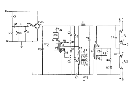
Fig. 3 is a circuit schematic of the dimming
circuit of the present invention. The circuit operates as
follows: ac voltage is provided from a power source across
hot (H) to neutral (N). Diodes D1 and D2, resistor R1,
capacitors C1 and C2, and zener diode Z1 comprise a low
voltage do power supply. During each positive voltage
half-cycle, current flows from hot through capacitors C1
and C2, and diode D2 to neutral, charging capacitor C2
plus(+) to minus(-), as shown. Resistor R1 and zener diode
Z1 regulate the voltage on capacitor C2 so that the power
supply is essentially a do voltage source having a do
supply voltage equal to the breakover voltage of zener
diode Z1 and an internal resistance essentially equal to
6232-107.CN -7-
/lp/#11
20~2(~~~
R1. Diode D1 provides a discharge path for capacitor C1
during each negative voltage half-cycle.
Full-wave-bridge FWB rectifies ac voltage from the
power source and provides pulsating do voltage across the
output terminals (+) and (-). Pulsating do is filtered by
capacitor C3, which is connected across the output ter-
minals of the full-wave-bridge. Resistor R2 is connected
in parallel with C3 and bleeds charge from it when power
is removed. For purposes of this specification and the
appended claims, when referring to electrical elements, the
term "connected°' means that there exists between two or
more elements a conductive path, which may include addi-
tional elements not explicitly recited.
Diodes D3, D~, D5, and D6, MOSFETS Q1 and Q2,
resistors R3 and R4, transformer T1, and capacitor C4
comprise a switching inverter for switching and inverting
filtered do voltage into a high-frequency ac driving
voltage. During operation, capacitor C4 charges up to
approximately half of the voltage across capacitor C3.
When Q1 is conductive, a driving voltage is applied across
the primary winding P of transformer T2 that is positive
and equal to the voltage across C3 less the voltage across
C3 less the voltage across C4 (approximately half the
voltage across C3). When Q2 is conductive, the driving
voltage is inverted and equal to the voltage across C4.
When Q1 and Q2 are alternately switched at a high-frequency
(~27kHz), rectangular pulses of ac driving voltage are
produced having a peak-to-peak voltage substantially equal
to the voltage across capacitor C3.
The driving frequency is preferably between 20kHz
and 50kHz and is determined by the ac control voltage from
the PDM circuit, IC1, discussed below. Frequencies below
20kHz are in the human audible range and are therefore
undesirable. High frequencies above 50kHz are undesirable
because they tend to cause high thermal dissipation in
6232-107.CN -8-
/lp/#11
203~;0~8
MOSFETS Q1 and Q2 and they lower the capacitive impedance
of the fixture wires to ground.
Resistors R3 and R4 damp oscillations which may
otherwise occur due to the leakage inductance of secondary
windings S1 and S2 of transformer T1 and gate capacitance
of MOSFETS Q1 and Q2. Diodes D3 and D4 block reverse
current from flowing through MOSFETS Q1 and Q2, respective-
ly. Diodes D5 and D6 provide a commutation path for
current flowing through Q2 and Q1, respectively.
Q1 and Q2 could be any type of semiconductor
switch, such as FETS or bipolar transistors: however,
MOSFETS, as shown, are preferred because of their fast
switching ability and their relatively iow gate current
requirements. Alternatively, the switching inverter may be
replaced with a less-expensive semiconductor do frequency
converter, which converts a non-pulsating do voltage into a
high-frequency pulsating do voltage. An inverting type of
oscillating circuit, which converts do to ac, is preferred,
however, since it provides reduced peak magnetic flux in
the core of the power-carrying transformers for the same
amount of transformed energy.
Pulse duration modulation circuit PDM receives
voltage (+VDC) from the do power supply and provides an ac
control voltage across the primary winding P of transformer
T1 to control the conductivity of MOSFETS Q1 and Q2 and,
accordingly, the duration of each rectangular pulse of
driving voltage. Secondary windings S1 and S2 of trans-
former T1 are arranged so that voltage is applied to the
gates of MOSFETS Q1 and Q2 in opposite polarities so that
only one device may be conductive at any given time.
Pulse-duration-modulated driving voltage is provided across
primary P of transformer T2 and across the resonant circuit
consisting of inductor L1 and capacitor C5 connected in
series. The resonant circuit rings substantially sinusoid-
ally at the driving frequency with an amplitude determined
by the pulse duration of the driving voltage and the
6232-107.CN -9-
/lp/#11
203~05~
magnification factor Q of the resonant circuit. The
magnification factor Q, in this case, is determined primar-
ily by the impedance of lamps FL1 and FL2, which load the
resonant circuit in parallel.
Loading the resonant circuit in parallel tends to
stabilize operation of the gas discharge lamps. In par-
ticular, as current through the lamps increases, lamp
impedance decreases, decreasing the magnification factor Q
of the resonant circuit and, thereby, reducing its resonant
response. Conversely, as the current through the lamps
decreases, lamp impedance increases, increasing the mag-
nification factor Q of the resonant circuit and, thereby,
boosting its resonant response. The resonant circuit
essentially behaves like an ac current source and provides
high-frequency sinusoidal current through transformer T3 to
Lamps FL1 and FL2. The magnitude of the current is vari-
able from about 1 to 200mA RMS, depending upon the pulse
duration of the driving voltage, and is sufficient to
strike and maintain an electric discharge in the lamps.
To further increase the stability of the resonant
circuit, the frequency of the driving voltage (~27kHz) is
less than the peak response frequency of the resonant
circuit (~33kHz). Alternatively, damping could be added to
the resonant circuit, reducing the magnification factor Q:
however, this would reduce its efficiency and generate
unwanted heat.
Capacitor C6, resistors R5 and R6, and diode D7
form a back end rectifier circuit for providing do current
through lamps FL1 and FL2 in series. Capacitor C6, con-
nected between secondary windings S1 and S2 of transformer
T3, is selected to pass substantially all high-frequency
sinusoidal current from the resonant circuit to lamps FL1
and FL2. Resistor R6 allows do current to flow through
diode D7, providing a do offset to capacitor C6 so that the
sinusoidal current through C6 and lamps FL1 and FL2 re-
ceives a do component of current, as determined by resistor
6232-107.CN -10-
/lp/#11
2~3~,~5~
R6. Resistor R5 is essentially a bleeder to discharge
capacitor C6 when power is removed. Resistor R5 also
limits the amount of do offset on capacitor C6 when the
impedance of the lamps increases (at low power levels).
Earth ground is referenced between secondary
windings S1 and S2 of transformer T3. The relative sizes
of the secondary windings are selected to provide suffi-
cient voltage with respect. to ground to strike lamps FL1
and FL2 through the capacitance to ground of each lamp.
They are also selected to balance the ground currents
through each lamp so that the high-frequency sinusoidal
current energizes the lamps equally. In this particular
circuit, a compromise is necessary to achieve sufficient
striking voltage and, thus, the ground current through lamp
FL1 is slightly larger than that through FL2. To correct
for this imbalance, capacitor C7 is provided in shunt with
lamp FL1 to provide compensating current to lamp FL2.
Capacitor C8 prevents high-frequency switching noise from
MOSFETS Q1 and Q2 in the switching inverter from adversely
affecting the light output of lamps FL1 and FL2.
Secondary windings S1, S2, and S3 of transformer T2
provide voltage to the filaments of lamps FL1 and FL2 to
heat them. Primary winding P of transformer T2 receives
pulse-duration-modulated voltage from the switching in-
verter circuit including MOSFETS Q1 and Q2. In addition,
after Q1 is turned off and before Q2 is turned on, current
through Q1 and inductor L1 commutates through diode D6,
turning it on. This provides across primary winding P of
transformer T2 an additional pulse of voltage, having an
amplitude equal to the voltage across capacitor C4. Once
the voltage across capacitor C5 reaches its peak, current
reverses through inductor L1, and capacitor C5 discharges,
turning diode D5 on. This provides across primary winding
P a second pulse of voltage, having an amplitude equal and
opposite to that of the first pulse. The two additional
voltage pulses substantially occupy the period of time
6232-107.CN -11-
/lp/#11
~0320~~
after Q1 is turned off and before Q2 is turned on. The
circuit behaves similarly during the period after Q2 is
turned off and before Q1 is turned on. The resultant
high-frequency voltage across primary winding P has an Ri~IS
value that is substantially constant throughout the dimming
range of the lamps. Thus, secondary windings S1, S2, and
S3 also provide constant RMS voltage to heat the filaments
of lamps FL1 and FL2 throughout the dimming range.
Although the present invention is described for use
with compact fluorescent lamps, the circuit herein descri
bed may be used to control any type of gas discharge lamp.
Since certain changes may be made in the above described
circuits without departing from the scope of the invention
herein involved, it is intended that all matter contained
in the above description or shown in the accompanying
drawings shall be interpreted in an illustrative and not a
limiting sense.
6232-107.CN -12-
/lp/#11