Note: Descriptions are shown in the official language in which they were submitted.
'2 0 ~
- 1 - RD-19,885
STRucrrup~F~
3~ l s3~iQ~
The present application is related to Application
Serial No. ~RD-19,511), filed , entitled,
"Thin Film Transistor Structure With Improved Source/Drain
Contacts", by R.F. KwaQnick, et al. and Application Serial
No. IRD-19~810)~ filed , entitled, "Thin
Film Transistor Having an Improved Gate Structure and Gate
Coverage by the Gate Dielectric" by R.F. Kwasnick, et al.,
each of which is incorporated herein by reference.
Ba~k~roun~ In~Qxma~iQn
The present invention is related to the field of
photosensitive imaging arrays, and more particularly, to such
imaging arrays which incorporate thin film transistors for
control of readout.
~=~ ~
A variety of photosensitive imager arrays are known
in the art. One type of photosensor array comprises a
substrate having an array of amorphous silicon (a-Si) thin
film transistors (TFT's) disposed thereon. The thin film
transistors, in turn, have an array of amorphous silicon
photodiodes disposed thereover and in contact therewith, with
one photodiode associated with and connected to each thin
film transistor. Such imagers can be fabricated with a
relatively high density of relatively small photosensitive
cells and can be made much larger in area as compared to such
photosensor arrays fabricated in monocrystalline silicon. As
a consequence, such imagers have found application in a
number of products. The most common form of such a
photosensltive array employs inverted thin film transistors
.
,', '
,
20~78~
- 2 - RD-19,885
and in sequence from the substrate up, comprise a ga~e
electrode pattern disposed on the substrate and con~igured to
serve as a scan line for a ro~l of thin film transistors by
connecting the gates of all o~ the thin film transistors on a
row in parallel, a gate dielectric overlylng the gate
electrode pattern and eY.posed portions of the substrate, a
layer of intrinsic amorphous silicon having a thinner layer
of N+ doped amorphous silicon disposed thereon with that
silicon layer being patterned to provide the thin film
transistors of the readout system, a layer of source/drain
metallization disposed over the layers of semiconductor
material and patterned to provide the source and drain
electrodes of the individual thin film transistors and to
couple a column of thin film transistors in parallel to a
data scan line integral with the drain metallization of the
transistors of that column. The source electrodes are
individually isolated to individual cells. A second layer of
amorphous silicon overlies this structure and is patterned to
be restricted to individual segments, each disposed in ohmic
contact with the source eiectrode of its associated thin film
transistor. That source electrode serves as the bottom or
readout contact for that photodiode. The upper contact for
the photodiodes is typically a transparent conductor which
makes contact to all of the diodes.
While such photosensitive arrays are successfully
fabricated at reasonably low cost, there are yield problems
in the fabrication of such arrays which increase the cost of
the individual arrays. One of the yield problems is that
during patterning of the amorphous silicon which forms the
photodiodes, the etchant finds its way through weak or open
spots in the passivation layers overlying the underlying thin
film transistor array and, therefore, etches exposed portions
of the silicon of the thin film transistors and exposed
portions of the source/drain metallization of those devices
with consequent impairment of the operating characteristics
,:
. :
,
: ~"' . . '.
,
. ,. ~
87~S
_ 3 - RD-19,885
of the array including, in many cases, inoperativ~ness of
particular picture elements ~pixels) of the array as a resulc
of unintended open circuits.
An improved structure or the thln fiLm transistors
of such a photosensitive array and o~ the photosensitive
array itself is needed which facilitates fabrication of such
arrays with greater yield and higher reliability.
Q~jects of the Invention
Accordingly, a primary object of the present
invention is to provide a thin film transistor structure for
photosensitive arrays which has increased immunity to
deterioration during patterning of overlying semiconductor
material.
Another object of the present invention is to
provide a photosensitive device semiconductor layer
configuration which results in improved reliability and ease
of fabrication of a photosensitive array employing thin film
transistors.
Another object of the present invention is to
provide an improved method for fabricating thin film
transistor photosensitive arrays which results in simplified
fabrication and hlgher yield.
~ ~ 3~ D~_L~
The above and other objec~s which will become
apparent from the specification as a whole, including the
drawings, are accomplished in accordance with the present
invention by changing the retention pattern for the
semiconductor layer in which the thin film transistors are
fabricated. This semiconductor layer is configured in
accordance with the intended source electrode pattern so that
it underlies the entire area occupied by the source electrode
for that thin film transistor and the entire area occupied by
the semiconductor material of the overlying photosensitive
, ,~
,
.
. ~ , .
2 0 ~ ~ r~ ~3 r~
- 4 - RD-l9~ ~385
device. In particular, instead of patterning the
semiconductor material of which the thin ~ilm transistors are
formed to minimize the overlap of the source metallization on
that material, that rnaterial is intentionally pakterned ~o
underlie the entire area occupied by the source electrode.
This change in semiconductor layer configuration eliminates a
step in the source electrode whlch is typically on the order
of 2, 500A high where the source electrode extends beyond the
edge of the thin film transistor semiconductor material in
the prior art configuration. That step in the prior art
structure is a location where many faults and opens occur as
a result of inadequate passivation of the source
metallization and the semiconductor material of the thin film
transistor.
Bri~e~ri~iOn of~th~ ~r~in~
The subject matter which is regarded as the
invention is particularly pointed out and distinctly claimed
in the concluding portion of the specification. The
invention, however, both as to organization and method of
practice, together with further objects and advantages
thereof, may best be understood by reference to the following
description taken in connection with the accompanying
drawings in which:
Figure 1 is a plan view illustration of a portion
of a~prior art thin film transistor photodiode photosensitive
array;
Figures 2 and 3 are cross-sections taken through
the structure of Figure 1 along the section lines 2-2 and 3-
30 3;
`- Figure 4 is a plan view illustration of a similar
portion of a thin film transistor photodiode photosensitive
array in accordance with the present invention; and
. . .
., . ~ , . ..
.
` 20~7~
- 5 -- E~D--19, 885
Figures 5 and 6 are cross~sections through the
structure of Figure 4 taken along the lines 5-5 and 6-6 in
Figure 4.
~ C~ 4cLi~Ll~
In Figure 1, a portion of a prior art thin film
transistor photodiode photosensitive array is illustrated in
plan view. The central por~cion of this illustration is one
pixel 160 of such a photosensitive array and has adjacent
thereto small segments of the adjacent pixels to more clearly
illustrate the overall configuration of the device. This
same structure is illustrated in cross-section in Figures 2
and 3 which are taken along the lines 2-2 and 3-3 in Figure
1. As is apparent from Figures 2 and 3, the structure shown
in plan view in Figure 1 has a plurality of levels. In the
center of the pixel 160 is a relatively large, usually
rectangular ~and typically substantially square) segment 150
of semiconductor material in which the photosensitive device
for that cell is fabricated. Directly below that is the
source electrode 138 for the thin film transistor associated
with that cell which lies within the picture frame of the
lying semiconductor material except in the upper left corner
of the pixel 160. It will be understoodr that these thin
film transistors are symmetrical and either electrode could
2S be called the source electrode. The selected designation is
therefore arbitrary and has been chosen so that the drain
electrode serves as the data line for the column of cells
since data and drain both start with the letter "d". In the
upper left-hand corner, the source metallization 138 includes
a projection which extends over the semiconductor material
130-132 of the thin film transistor and overlaps sligh~ly
with the gate metallization 118 for that transistor. The
gate metallization 118 is disposed on the substrate 112 and
is the lowest level portion of the structure identified in
Figure 1. The source/drain metallization of the thin film
i ~ . ;
.
- 6 _ ~ R~-19,885
transistor also includes stripes which extend vertically in
the figure which are disposed on either side of the pixel
160. These conductors are known as data lines in the thin
film transistor photosensitive array art. Each data line
includes a projection which extends over the gate electrode
of the thin film transistor for each pixel in the column
served by that data line. In this manner, any data read out
of any of the photosensitive cells in that column appears on
that data line. The gate metallization 118 is common to all
of the thin film transistors in a given row of this array and
is known as a scan line. Applying a voltage to the gate
metallization which renders the associated thin film
transistor conductive causes whatever charge is stored in the
photodiode as a result of the light impinging thereon to be
transferred from the source electrode which is in contact
with the lower surface of that photodiode to the data line.
In this manner, all cells in a given row of this array are
read out simultaneously with their data appearing on the
corresponding column data lines. Referring more particularly
to Figure 2, the step in semiconductor material height where
the semiconductor material ends is identified by the
reference numeral 133. This point is also illustxated in
Figure 1 at the upper left corner of the pixel 160 where the
source electrode extends over the semiconductor material to
25 reach its overlap with the gate electrode.
In a typical thin film transistor, the gate
metallization is about 1, 800A thick, the gate dielectric is
about 1500A thick and the semiconductor material is about
2,500A thick.~ The source/drain metallization is typically
4000A thick. Consequently, with the vertical step at the
edge of the semiconductor material which is typically
produced by many fabrication processes, the source electrode
extends over a step which is about five-eighth its own
thickness. The source metallization is typically retains a
substantially vertical edge which is difficult to adequately
, . .
-
2 ~
- 7 - RD-19,885
passivate. The problems crea~ed by this step are further
exacerbated by the tendency of the source metallization to
etch, during the etching of the source metallization, at a
faster rate along steps, probably due to stress in the source
metal going across the step. This forms a notch in the
source metallization which can be particularly dificult to
protect from subsequent etch steps required in the imager
fabrication process. As a consequence of these effects, the
passivation layer 148 which extends over this step in the
source metallization has a significant propensity or
penetration by the etchant which patterns the overlying
semiconductor material. The effect of such penetration
varies with the degree of passivation present prior to the
beginning of the etching process and can vary from slight
deterioration in the operating characteristics of the device
to the creation of an open circuit which renders that pixel
of the device inoperative. While in many applications a few
inoperative pixels can be tolerated, they are considered
undesirable even in those applications and are not permitted
in many other applications. Consequently, there is a need to
improve the structure and process for fabricating such thin
film transistor photodiode imaging arrays to eliminate or
minimize the tendency for the patterning of the overlying
semiconductor material of the photosensitive devic~ to result
in deterioration of the source electrode, the underlying
semiconductor material or other portions of the structure as
a result of inadequate passivation of such steps.
In accordance with the present invention, this
problem is overcome by changing the pattern used to pattern
the semiconductor material of the thin film transistor. In
particular, rather than the semiconductor material of the
thin film transistor being patterned to stop at the edge 133
as has been done in the prior art, this edge is eliminated by
patterning the semiconductor material to underlie the entire
source electrode of that transistor and the entire
~0~3~
- 8 - RD-19,8~5
semiconductor material of the photosensitive device for that
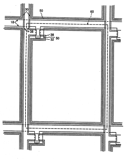
pixel of the array. Thus, as illustrated in the plan vie~7 in
Figure 4, the semiconductor material 32 extends into the
interior of the pixel from the gate electrode protrusion into
that pixel and forms a substantially rectangular picture
frame 32 around the source electrode 38 for that pixel The
semiconductor material of the photosensitive device forms a
picture frame around both the ~ource metallization and the
underlying semiconductor material, except where they extend
out to the active area of the thin film transistor in the
upper left portion of the pixel 60. For optimum device
characteristics, it is preferred to fabricate the gate
electrode material for this array as a two layer conductor
comprised of chromium as a thin first layer and molybdenum as
a thick second layer as taught in related Application Serial
No. ~RD-19,810), entitled, "Thin Film Transistor
Having an Improved Gate Structure and Gate Cov~rage by the
Gate Dielectric". It is also preferred to ~abricate-the
source/drain metallization as a two layer structure having a
thin first layer of chromium and a relatively thick second
layer of molybdenum as taught in related Application Serial
No. (RD-19,511), entitled, "Thin Film Transistor
Structure for Uniform Characteristics Across a Wafer and
Method of Fabrication", in order to provide a sloped sidewall
on the source/drain metallization which facilitates the
passivation of those sidewalls by a subsequently deposited
passivation layer 48.
This inventive structure may be fabricated in
substantially the same manner as the prior art structure with
but with a change in the configuration of the semiconductor
material of the thin film transistors.
While it is preferred to have the source electrode
disposed entirely on the semiconductor material of the thin
film transistor as has been described, many of the resulting
benefits can be obtained by locating the edge of the
'' '
.
, . ,
20~8~
- 9 - RD-19,885
semiconductor material of the thln film transistor far enough
under the semiconductor material of the photosensitive device
that the step in the source electrode is protected from
exposure to the etchant used to pattern the semiconductor
material of the photosensitive device by both that
semiconductor material itself and the photoresist which
protects those portions of that semiconductor material which
are to be xetained in the final device structure. This
eliminates the risk of ineffective passivation of the step in
the source metallization resulting in penetration by the
semiconductor etchant.
While the invention has been described in terms of
its use with amorphous silicon, it will be understood that
the invention is applicable to any similar structure whether
made from silicon or other semiconductor materials.
While the invention has been described in detail
herein in accord with certain preferred embodiments thereof,
many modifications and changes therein may be effected by
those skilled in the art. Accordingly, it is intended by the
appended claims to cover all such modifications and changes
as fall within the true spirit and scope of the invention.