Note: Descriptions are shown in the official language in which they were submitted.
-- 1 --
ELECTRONIC CIRCUIT PACKAGE
The present invention relates to the miniaturization of
an electronic circuit package, and, more particularly, to an
extra-small computer for use in space exploration~
A number of computers are being employed ~or various uses
and the demand for smaller and lighter computers has
increased. Computers for use in space are required to be
particularly small and light in order to decrease the
launching costs while increasing the payload.
As shown by a photograph 1 of "Development of LSI for
Radiation Resistant 16-Bit Microprocessor", pp. 10 - ~11, Goke
et al, Collection of Pap~rs at 32nd Space Science and
Technology Federation Lecture Meeting~ a space computer can be
built of discrete parts with reliable, resi~tant-to-
environment single chips contained in one package.
There is no serious consideration of decreasing the size
and weight of a computer comprised of discrete parts.
On the other hand, a so-called multiple chip mounting
technique, that is, the technique of mounting a plurality of
bare chips on one wiring substrate for use on the ground is
being studied. It has haretofore been arranged hat, as shown
in Fig. 3 of l'Nikkei Micro Device~, pp. 32 - 40, December
lssue, 1989, a wiring conductor connected to a bonding pad is
led out from the bonding pad.
Making the wiring density uniform was not considered in
this technigue. The wiring density around the die bonding pad
in particular is extremely high and consequently effective
wiring cannot be implemented. The wiring density in the
outermost layer causes a bottleneck and the package size is
not sufficiently reduced. As the hole connecting the upper
and lower layers occupied most of the area on this particular
multilayer wiring substrate, the holes account for a large
percentage of the area of the outermost layer, particularly
around the die bondiny pad.
,, ~,
.~
t ' ~ ~
' ' , ~ ,
: ' , ':: ' ~ , ' '
With respect to a faulk tolerant system, a checking unit
for detecting errors and faults and a unit under check are
accommodated in one and the same chip to reduce its size, as
described in "Trial Manufacture and Evaluation of Fault
Tolerant Quartz Oscillation IC", by Tsuchimura et al, Research
Material, 24th FTC Study Meetiny. With the diffusion of ASICs
(Application Specified ICs) in particular, attempts have been
made to add an MPU inspsction circuit by making an ordinary
MPU a core through the ASIC technology.
Faults and trouble affecting the whole chip were not
taken into consideration in this technique. If the checking
unit and the unit under check develop trouble simultaneously,
the irregularity may not be detected.
An object of the present invention is to provide a small
and light electronic apparatus, in particular an electronic
circuit package, with high reliability.
Another object of an embodiment of the present invention
is to provide a small and light electronic apparatus in which
the number of pins affixed to the outside of the package is
reduced to prevent an increase in the package size.
Further, another object of an embodiment of the present
invention is to provide a small and light electronic apparatus
in which the wiring density is eased to preYent an increase in
the package size.
To these ends, the invention consists of an electronic
circuit package comprising at least two semiconductor chips
that are all connected to a bus line and to a wiring
substrate.
Preferably the chips are bare chip packaged on the wiring
substrate, the semiconductor chips and the wiring substrate
being connected by wiring bonding between wire bonding pads
formed on the chips and the substrate. The substrate may be a
multilayer.
Preferably, the invention also provides an electronic
circuit package comprising a multilayer wiring substrate on
which at least one semiconductor chip is provided, an
insulating layer partially ~ormed on the surface of said
, ~
.
" :
-- 3 --
multilayer wiring substrate, and a die bonding ground ~ormed
on a surface of said insulating layer in order to use a
portion of said multilayer wiring ~ubstrate under said die
bonding ground as a wiring or hole region, wherein at least
one of said semiconductor chips is formed on said die bonding
ground.
The invention also consists of an electronic system
including such an electronic circuit package.
In the drawings:
Fig. 1 is an overall structural view of an embodiment of
the present invention;
Fig. 2 is a sectional view of a die bonding portion of a
wiring substrate according to an embodiment of the present
invention;
Fig. 3 is a diagram showing an arrangement of holes in an
embodiment of the present invention;
Fig. 4 is a diagram showing the division of a data bus in
an embodiment of the present invention;
Fig. 5 is a diagram showing the division of a data bus
having a 3~ bit width in an embodiment of the present
invention;
Fig. 6 is a structural view of an MP~ with a checking
circuit and a RAM with an error correction code on a wiring
substrate in an embodiment of the present invention;
Fig. 7 is a structural view of an MPU with an external
ROM on a wiring substrate in an embodiment of the present
invention;
Fig. 8 is a circuit diagram of electronic apparatus
according to the present invention;
Fig. 9 is a diagram showing packaging of semiconductor
chips as shown in Fig. 8 on one side of a wiring substrate;
Fig. 10 is a diagram showing packaging of semiconductor ~: ;
chips as shown in Fig. 8 on the other side o~ the wiring
substrate; and
Fig. 11 (with Fig. 1) is a sectional view of a package in
an embodiment o~ the present invention.
-~
.,
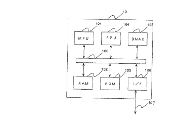
Fig. 1 illustrates the inner construction oE electronic
apparatus embodying the present invention by way of example.
In the embodiment shown, MPU 101, RAM 102, ROM 103, FPU
(Floating-point Processing Unit) 104, DMAC (Direct Memory
Access Controller) 105, and an interfac:e circuit 106 are
connected via a bus 100 in a wiring substrate 10. What is
particularly noticeable according to this embodiment is that
the bus loO is not led out of the wirirlg substrate lo, but
only an interface line 107 for connection to external devices
is led out of the substrate 10.
All semiconductor chips connected to the bus 100 are
totally packaged on the wiring substrate 10 according to this
embodiment. As the bus 100 is not led out of the substrate
10, the number of signal lines connecting internal and
external devices is reduced by a large margin. Accordingly,
the number of pins connecting the signal lines inside and
outside the wiring substrate 10 decreases and this avoids an
obstacle to rendering the wiring substrate smaller and
lighter.
Fig. 2 is a sectional view of a die bonding portion of
the wiring substrate 10. Wire bonding pads 11 are formed on
the substrate 10 and an insulating layer 16 is formed on a
wiring conductor 14 for use in leading out the wire bonding
pad. A die bonding ground 15 is formed on the insulating
layer 16, and a semiconductor chip 20 is bonded thereto by die
bonding. A bonding wire 30 is then used for connecting a wire
bonding pad 21 on the semiconductor chip 20 to the wire
bonding pad 11 on the wiring substrate 10. According to this
embodiment, as shown in Fig. 3, holes 13, 13' may be formed in
the periphery and inside of the die bonding ground 15,
respectively. The hole 13 formed in the periphery of the die
bonding ground 15 and the wire hole 13' formed inside the die
bonding ground 15 are preferably arranged alternately. As a
result, a portion beneath the die bonding ground 15 as the
outermost layer that has heretofore been unutilized can be put
to practical use as a wiring and a hole region. An area to be ,~
occupied by the wiring and hole regions can thus be made
'
-- 5 --
drastically smaller than the area occupied by the
semiconductor chip of the wiring ~ubstrate.
Fig. 4 re~ers to an embodiment wherein signal lines o~
the data bus 100 connected to the MPU 101 are divided into two
groups 100-l and 100-2. RAMs 102-1 - 10~i-k and ROMs 103~1 -
103-k connected to the data bus 100-l are packaged on one side
(B side? of the substrate, while RAMs 102-(k + 1) - 102-N,
ROMs 103-(k +1) - 103-N connected to the data bus 100-2 are
packaged on the other side (A sid~) of the substrate, wherein
k and N is each an integer. According to this embodiment, it
is unnecessary to connect the data bus on the A side to what
is on the B side and hence the number of holes in a wide area
can be reduced. As a result, an area to be occupied by wiring
and hole regions can thus be made drastically smaller than the
area occupied by the semiconductor chip of the wiring
substrate, so that the apparatus can be made smaller and
lighter.
Fig. 5 refers to an embodiment in which the data bus 100
connected to the MPU lOl is 32 bits wide and the data bus
connected to the ROM and RAM is 8 bits wide. Data lines D0 -
D31 constituting the data bus 100, D0 - D15 are formed into a
group of data bus 100-1, and lines D16 - D31 into a group of
data bus 100-2. Lines D0 - D7 in the group of data bus 100-1
are connected to the RAM 102-1 and the ROM 103-1, and lines D8
- D15 to the RAM 102-2 and the ROM 103-2. Moreover, lines D15
- D23 in the group of data bus 100-2 are connected to the RAM
102-3 and the ROM 103-3, and lines D24 - D31 to the RAM 102-4
and the ROM 103-4. Accordiny to this embodiment, the
appara'us can be made smaller and lighter as in the case of
the embodiment shown in Fig. 4.
According to the embodiments shown in Figs. 2 to 5, it is
also possible to package as many bare chips as possible on the
wiring substrate that is limited in size.
Fig. 6 refers to an embodiment wherein the MPU 101, a
checking circuit 111 of the MPU 101, and the RAM 102 and an
error correction code encoding/decoding circuit 112 are
packaged in the form of bare chips on the wiring substrate 10.
. . .
. "
- . ' ~': ',',.' ' '
. ~ ' '' ~
In this case, the bonding wire has been omitted for
simplification.
The MPU 101 and the checking circuit 111 are different
bare chips and are connected by wire bonding on the wiring
substrate 10. Heretofore, various systems have been proposed
for the checking circuit 111. There are the following, for
instance:
(1) A watch dog timer for resetting the MPU 101 after
sensing its operation on an impulse when it is unaccessible
within a fixed period of time.
(2) A system having a reference MPU (not shown) within
the checking circuit 111 for comparing the output signal o~
the reference MPU with that of the MPU 101, regarding the
reference MPU or the MPU 101 as irregular when nonconformity
is found.
In the conventional method of packaging the MPU 101 and
the checking circuit 111 separately, the number of packages,
the number of wires and the dimensions of the apparatus tend
to increase. In the method recently followed for forming the
MPU 101 and the checking circuit 111 on the same chip,
moreover, a fault involving the whole chip is not completely
detectable as even the checking circuit 111 then ceases to
function.
According to this embo~;r~nt, the MPU 101 with the
checking circuit 111 is capable of detecting a ~ault involving
the whole chip without causing the number of packagDs and that
of wires to increase. Therefore, a small lightweight, ;
reliable apparatus can be achieved.
The RAM 102 and the error correction code
encoding/decoding circuit 112 are different bare chips and are
connected by wire bonding on the wiring substrate 10.
The error correction code adds an error
detection/correction redundant bit to the data stored in the
memory, thus causing an error to be detected and corrected by
making a code-to-code ~rm; ng distance 4 or greater. When the
code-to-code ~ ;ng distance is set to 4, 1-bit error
correction is possible, but a 2-bit error remains only
.... ~, '
~ ~ '
-- 7
detectable. Consequently, it is called SECDED (Single-Er~or-
Correction, Double-Error Detection). For instance, a 6-bit
detection~correction redundant bit needs to be added when
SECDED is to be realized for 16-bit data. A detailed
description of an error correction code is omitted since the
present invention is not concerned therewith.
In the conventional method of packaging the RAM 102 and
the error correction code encoding/decoding circuit 112
separately, the number of packages, the number of wires and
the ~;r-n~ions of the apparatus tend to increase. In the
method recently followed for forming the R~ 102 and the error
correction code encoding/decoding circuit 112 on the same
chip, moreover, a fault involving the whole chip is not
completely detectable as even the error correction code
encoding/decoding circuit 112 then ceases to ~lmction.
According to this embodiment, the RAM 102 with the error
correction code encoding/decoding circuit 112 is capable of
detecting a fault involving thP whole chip without causing the
number of packages and wires to increase. Therefore, a small
lightweight, reliable apparatus can b~ achieved.
Like other semiconductor elements~ the storage element
(ROM) storing the program involved is packaged on the same
wiring substrate in the form of a bare chip, and, if it is
incorporated into the same package, the apparatus can be made
drastically smaller and lighter. If the ROM is incorporated
into the package, it will require to devise its programming
and erasing methods. Use of an ~PROM (Electrically Erasable
Programmable ROM~ will make programming readily possible and
make the program erasable. Even when a W EPROM (Ultra-Violet
Erasable Programmable ROM) is used, the program can be
executed or erased by providing the apparatus with a window
that allows erasiny ultra-violet rays to pass therethrough.
When an EPROM is used as space electronic apparatus to be
exposed to cosmic rays, the data written by the cosmic rays
may be erased. Moreover, an EPROM is not suitable ~or use in
an electronic apparatus to be used over several hundred
thousand years, due to the electronic thermal movement.
i:
,~
.
, '. ,-, '
'' :
~ .
: - ~ ,.
Therefore, mask- or fuse~RVMs will have to be used ~or this
purpose.
For program development, the program involved has to be
modified and rewritten. For this reason, a mask- or ~use-ROM
may not be used e~ficiently for such program development.
According to the ~ollowing embodiment of the present
invention, the electronic apparatus leads the line connecked
to the ROM out of the package and makes it possible to operate
the ROM outside the package. Consequently, no wire bonding is
provided for the ROM in the developing package. By connecting
a program externally, that is, its easily erasable EPROM to an
external device, any program may be developed by means of a
wiring substrate having the same pattern as that proposed in
the present description.
Fig. 7 refers to an embodiment wherein either the ROM
inside the wiring substrate 10 or an external ROM can be used
to operate the MPU. The RAM 102 and the ROM 103 are connected
to the MPU 101 via the bus 100 in the wiring substrate 10.
Moreover, the RAM 102 and the ~OM 103 selection siynals CS#
are formed by an address decoder 107. Although a signal name
with a line thereon is provided for each active low signal in
Fig. 7, a signal name followed by a '#' mark is employed in
this specification for convenience of description. The
address decoder 107 decodes higher significant bits in an
address signal supplied to the bus 100, and, when the address
signal indicates the address of the RAM 102 or the ROM 103,
applies the corresponding selection signal CS# to the R~M 102
or the ROM 103. While the selection signal CS# is active, the
RAM 102 or the ROM 103 reads or writes the desired address
data in accordance with the lower significant bits.
According to this embodiment, a ROM 103 selection signal
~S# 108 is also sent out of the wiring subskrate 10.
Conse~uently, a ROM 103' outside the wiring substrate 10 in
place of the ROM 103 inside the wiring substrate 10 can be
used for operation. Moreover, since part of the lower
significant bits in the address bus signal is enough for an
address line to be connected to the ROM 103', the number of
leader lines from the wiring substrate 10 is also prevented
from increasing~ In order to develop a program, it is only
necessary to write the program to the ROM 103' outside the
wiring substrate 10 without packaging the ROM 103 inside the
wiring substrate 10. Hence, e~ficient program development can
be made, as a program is readily written to and erased ~rom
the RON. If a mask- and a fuse-ROM are used as the ROM 103
inside the wiring substrate 10 for an actual apparatus a~ter
program development, any ~ear of erasure of the data in the
ROM 103 is eliminated and the appara1us stands to remain in
good condition after long use.
Fig. 8 is a circuit diagram embodying the present
invention. The MPU 101, RAM 102, ROM 103, FPU 104, D~AC 105,
and a gate array 110 in the ~orm of bare chips are mounted on
the wiring substrate 10. Although the RAM 102 and the ROM 103
consist of a plurality of chips, depending on the memory
capacity and bit width, each o~ them is indicated as one in
Fig. 8 for simplicity. In the gate array 110 are the checking
circuit 111 formed with the watch dog timer or the like for
detecting the opPration of MPU on impulse, the error
correction code encoding/decoding circuit 112 ~or correcting
the inversion of data in the RAM 102, the address decoder 107,
and the interface circuit 106 with external devices or the
like as built-in elementsO (These circuits in the gate array
are not shown in Fig. 8.) The number o~ chips can thus be
reduced significantly, as the peripheral circuits o~ the MPU
101 are arranged in such a gate array form.
As the checking circuit 111 and the error correction code
encoding/decoding circuit 112 are accommodated on chips
different from those for the MPU 101 and RAM 102 with respect
to the gate array 110, failure to d~tect a ~ault involving the
whole chip is avoided.
Although use can be made o~ various kinds o~ respective
MPU 101, FPU 104, DMAC 105, the illustration o~ Fig. 8 is
based on the assumption that a GMICRO/200 (H32/200~ series is
employed. Consequently, the names of the various control
signal lines are indicated in accordance with the
.
~ 10 --
specification of the GMICRO/200 (H32/200) series. Since the
present invention is not limited to a particular product
series, the description of the signa:L names is irrelevant to
the present invention and are omitted; a detailed description
of them has been given in a document ('H32/200 Hardware
Manual', Hitachi Ltd.). Incidentally, the bit positions of
the address and data lines are provided in the form of a
bigendian display and the lower significant bits are therefore
expressed by small numbers. For instance, A0 of the address
line represents the highest signiEicant bit, whereas A29
represents the lowest significant bit;.
The bus signal lines led out of the wire substrate 10
according to this embodiment are only as follows: address
lines A13 - A29, data lines D0 - D31, address strobes ASl#,
AS2#, byte control signals BC0# - BC2#, a read/write switching
signal RJW# and a data transfer termination signal Dc#. In
other words, since only a part of the bus signal lines is led
out of the wiring substrate 10, the number of pins affixed to
the outside of the package can be reduced so that the package
size can be made smaller. If it is decided not to use ROMs
outside the wiring substrate 10, all of these bus signal lines
need not necessarily be led out. Thus, the number of pins can
be reduced.
The address decoder 107 (not shown) in the gate array
generates the ROM selection signal ROCS#108, a RAM selection
signal RACE0# - RACE3#, and an external element selection
signal XCS# by means of the address lines AO - A12.
The ROM selection signal ROCS#108 on one of these signal
lines is connected to the R~M 103 in the wiring substrate 10
and is simultaneously led out of the wiring substrate 10.
According to this embodiment, the ROM 103' (not shown) in
placa of the ROM 103 inside the wiring substrate 10 can be
connected to the outside of the wiring substrate 10 and used
for operation. Moreover, since a part of thP lower
significant bits A13 - A29 in the address bus signal is enough
for an address line to be connected to the ROM 103', the
number of leader lines from the wiring substrate 10 is also
,;. .
. ~ .
':
prevented ~rom increasing. In order to develop a program, it
is only needed to write the program to the ROM 103' outside
the wiring substrate 10 without packaging the ROM 103 inside
the wiring substrate 10. Hence, efficient program development
can be achieved, with a program being readily written to and
erased from the ROM. If a mask- and a fuse-ROM is used as the
ROM 103 inside the wiring substrate 10 for the apparatus after
the program development, any risk of erasure of data in the
ROM 103 is eliminated and the apparatus can be expected to
remain in good condition after long use.
The RACE0# - RACEl# out of the RAM selection signals
RACE0# - RACE3# are connected to the RAM 102 inside the wiring
substrate 10, whereas the RACE2# - RACE3# are led out o~ the
wiring substrate 10. If the RACE2# - RACE3# are led out of
the wiring substrate 10, the byte control signal BC0# - BC2#,
the read/write switching signal R/W#, the address lines A13 -
A29 and the data lines D0 - D31 are connected to a RAM 102'
(not shown) outside the wiring substrate 10, and an increa~e
in the storage capacity can be attained with the combination
of the RAM 102 and the RAM 102'.
The external element selection signal XCS# is led out of
the wiring substrate 10, and, if the external element
selection signal XCS#, the byte control signal BC0# - BC2#,
the read/write switching signal R/W#, the address strobes
ASl#, AS2#, the data transfer termination signal DC#, the
address lines A13 - A29 and the data lines D0 - D31 are
connected to an external element (not shown), the system will
be improved as the external element becomes usable.
The number of pins may be drastic~lly reduced when the
external element is not connected as the RAM selection signals
RACE2# - RACE3#, the selection signal XCS#, the byte control
signal BC0# - BC2#, the read/write switching signal R/W#, the
address strobes ASl#, AS2#, the data transfer termination
signal DC#, the address lines A13 - A29 and the data lines D0
- D31 are unnecessary to lead out of the wiring substrate 10
to the RAM 102' outside the wiring substrate 10.
.
, :
, ,
. ' ' " - - . :
. ,
- 12 -
In addition, the gate array ~lo can be allowed to
incorporate the interface circuit 106 with external devices.
A signal line MIL - 1553B is employed for use in the so-called
MIL ~ 1553B communication standard. Moreover, a communication
line CELLCOMCNTR is a communication line for coupling a
plurality of computer units, each having the wiring substrate
10. If the number of wiring substrates 10 required is
prepared for the communication lines CELLCOMCNTR to be
connected together, it will facilitate the construction o~ a
multiprocessor system or a multiplex computer system for fault
tolerance.
Figs. 9 and 10 illustrate methods o~ packaging a wiring
substrate 10 embodying the apparatus shown in Fig. 8.
The MPU 101, FPU 104, ROMs 103-1, 103-2 and RAM 102-1,
102-2 are mounted on the surface (B side) shown in Fig. 9O
The storage element, the ROMs 103-1, 103-2 and the RAMs 102-1,
102-2 connected to the data lines which belong to the bus 100
1 are mountad on this surface, as shown in Fig. 5.
The DMAC 105, the gate array 110, the ROMs 103-3, 103-4
and the RAMs 102-3, 102-4 are mounted on the sur~ace (A side)
shown in Fig. 10. The storage element, the ROMs 103-3, 103-4
and the RAMs 102-3, 102-4 connected to the data lines which
belong to the bus 100-1 are mounted on this surface as shown
in Fig. 5.
Since the number of wiring layer-to layer holes can be
reduced according to this embodiment, the wiring substrate 10
can be made smaller. Moreover, the concentration of heat and
wiring on one side can be avoided by splitting the LSI, MPU
101, FPU 104, DMAC 105 and the gate array 110 into two groups,
each having a large chip size and many input-output signal
lines, and allotting them to the respective sides. In view of
thermal resistance, chemical stability and the like, a ceramic
substrate is suitable for uS8 as the wiring substrate 10 when
it is employed in space where reliability is required.
Fig. 11 illustrates a package embodying the present
invention. Ceramic caps 50 are attached to the respective
sides of the ceramic wiring substrate 10 to hermetically seal
- '
.~
,
~ 13 ~
the bare chips, such as the MPU 101 mounted thereon. 'rhe
inside thus hermetically sealed by the caps 50 is kept under a
vacuum or is filled with an inactive gas/ such as nitrogen,
helium or the like. If helium is used, it will conveniently
be used for leakage checking when the airtightness of the seal
is checked. When it is desired to accommodate a plurality of
chips in a single package, the package tends to become large
and the volume of air inside the capr, 50 also tends to
increase. Whsn the ceramic caps 50 are attached to the
respective sides of the ceramic wiring substrate 10 before
being used to hermetically seal the contants by soldering, the
molten solder may be drawn into or jutted out of the caps 50
due to the difference in pressure between the inside and the
outside as the solder cools. One o~ the measures to be taken
to prevent the molten solder from being thus drawn into or
jutted out o~ the caps 50, even though the package is large,
is to bore ventilating holes 51 into them and to cover the
holes 51 with lids 52 or the like after the contents have been
hermetically sealed with the inactive gas encapsulated.
According to the present invention, a plurality of
semiconductor elements can be accommodated in a single package
and the numb~r of signal lines to be led out of the package
can be reduced so that the package size is decreased. A small
lightweight apparatus is thus made available.
. ,~ ~ .
; .
.
.: !