Note: Descriptions are shown in the official language in which they were submitted.
20668~7
FLAT CAVITY RF POWER DIVIDER
BACKGROUND
The present invention relates generally to microwave tr~n~mi~sion systems and
more particularly to an RF power divider capable of hPn~lling relatively high power
with forced air cooling.
Cavity power dividers have proven to be the best suited colllponent to interfaceS with active phase array elements of satellite microwave ll~n~ ;on ~ntçnnP systems.
Prior RF power dividers are mostly co~ e feed types. The prior art includes either
waveguide tee junctions, or hybrid couplers. Square coaxial hybrid couplers are also
used as power dividers.
One example of a prior art power divider is described in a docum~nt entitled "4410 GHz Monolithic Conformal Active Transmit Phased Array Antenn~ " 1987, delivered
under contract number F19628-83-C-0115 by Harris Corporation. There is disclosed a
power divider consisting of a rectangular waveguide plate (parallel plate or Pillbox
Feed), a ridged waveguide to coaxial transition, a short section of ridged waveguide,
and coaxial to output port.
Another example of the pnor art is described in a docllm~nt entided "20 GHz
Monolithic Conformal Active Receive Phased Array .Antenn~ " March 1989, delivered
under contract number F19628-83-C-0109 by Ball Aerospace Corporation. The Ball
power divider consists of complex microstrip coupler power dividing circuits, wave-
guide-t~E-plane transidons, and mini-coax connected directly to microstrip as output
20 port. The disadvantages of these above-noted conventional devices include: low ther-
mal ~iissiration efficiency, complex cooling ~y~lellls, high mPnllfPcturin~sts, and
high RF insertion loss. ~
~ 0 ~ 7
SUMMARY OF THE INVENTION
In view of the foregoing factors and conditions characteristic of the prior art,it is an objective of an aspect of the present invention to provide a new and
improved flat cavity RF power divider. An objective of an aspect of the present
invention is to provide a light weight and less bulky flat cavity RF power divider.
An objective of an aspect of the present invention is to provide a compact flat cavity
RF power divider that may be forced air cooled and is simple in construction. Anobjective of an aspect of the present invention is to provide a flat cavity RF power
divider that provides desil~bl~ coaxial output ports for active elP-ment interfaces, and
that has a 5% bandwidth with smooth phase and ~mplitude output. An objective of
an aspect of the present invention is to provide a flat cavity RF power divider that
utilizes no tuning screws or ...At~ling reactors, and has a very thin profile of less
than l inch at 14.35 GHz.- An objective of an aspect of the present invention is to
provide a flat cavity RF power divider that implc~nPnt~ a l to 16 power division5 within a limited area, and is very suited to in~erf~-~e. with active phase array
elPmentc.
In accordance with an embodi..lent of the present invention, a flat cavity RF
power divider includes a flat cavity SlruCtu c having horizontal ce.lt~ lL~nc in a cavity
broadwaLI thereof, and upper and lower lon it~l~lin~l walls. An input waveguide struc-
ture having an input port at one end and a longitutlin,tl ce ~ e in a waveguide broad-
~ 20 wall thereof is also inc~ ed) the waveguide broadwaiU being shared with the cavitybroadwall, and the longitl..lin~l cent~line being pa~allel to and offset from the centerline
of the flat cavity ~L~u~;lui~e. Coupling means including a plurality of longit~lin~l shunt
slots are ~ pose~ in the common waLI along the cavity's longinl-lin~l centerline for
exciting a domin~nt TE~,o mode in the cavity's structure. The invention also includes
25 cwed waveguide short circuit means ~liciposecl in the waveguide structure for creating
a relatively high standing-wave along the waveguide sl~ucnue and provides a maximum
E-field to excite each of the slots and thereby excites the transverse axis column of the
flat cavity structure, and RF absorber means disjposed in the flat cavity ~ll ùClu~c along
the longitur1in~l walls thereof for frequency i~;s~onse improvement of the power30 divider. Output coupling means is also ~CSoci~t~d with the flat cavity structure for
providing an iRF power output.
The invention may be implemented wherein the input waveguide ~l. uctu.~ is a
WR-62 waveguide and the input port is at an outer end thereof. Alternatively, the input
waveguide structure may include an elong~t~ horizontal section and an elongated
35 ortihogonal feed section joining the horizontal section at a waveguide tee junction dis-
posed centrally along the horizontal section, the input port being disposed at an outer
end of the feed section.
` ~A. 2-
2~68~7
According to an embodiment of the invention, the coupling means
includes four longitudinal shunt slots spaced at multiples of quarter
wavelengths, and the output means may include 106 coaxial sub-miniature
adapter (SMA) output coupling probes extending into the flat cavity
structure and spaced about 1.5 ,19 apart.
Other aspects of this invention are as follows:
A flat cavity RF power divider, comprising:
a flat cavity structure having first and second opposed parallel
broadwalls and two opposed sidewalls and two opposed endwalls;
an input waveguide structure having an input port for receiving
electromagnetic energy and a first waveguide broadwall common with a
portion of said first flat cavity broadwall and a second waveguide broadwall
opposed to said first waveguide broadwall, said waveguide and cavity
structures being oriented such that a longitudinal centerline of said first
waveguide broadwall is generally parallel to and centrally disposed between
said sidewalls of said nat cavity structure;
coupling means including a plurality of longitudinal shunt slots
disposed in said first waveguide broadwall along a longitudinal slot centerline
which is parallel to and offset from said input waveguide centerline for exciting
in said cavity structure a dominant TE4 o mode of electromagnetic energy
input into said input waveguide structure;
curved waveguide short circuit means disposed in one end of
said waveguide structure opposite said input port of said waveguide structure;
and
a plurality of output coupling means disposed in said second
cavity broadwall for providing RF power output by coupling electromagnetic
energy from said flat cavity structure through said second cavity broadwall.--
- 3 -
2~8~7
A flat cavity RF power divider, comprising:
a flat cavity structure having first and second opposed parallel
broadwalls, two opposed sidewalls and two opposed endwalls;
an input waveguide structure having first and second waveguide
sections coupled at a tee junction, said second waveguide section having an
input port for receiving electromagnetic energy at one end and said tee
junction at the other end, said waveguide sections each having a first
waveguide broadwall common with a portion of said first flat cavity broadwall
and a second waveguide broadwall opposed to said first waveguide broadwall,
said waveguide and cavity structures being oriented such that a longitudinal
centerline of said first waveguide section broadwall is generally parallel to and
centrally disposed between said sidewalls of said flat cavity structure;
coupling means including a plurality of longitudinal shunt slots
disposed in said first waveguide section broadwall along a longitudinal slot
centerline which is parallel to and offset from said first waveguide section
centerline for exciting in said cavity structure a dominant TE4 o mode of
electromagnetic energy input into said input waveguide structure;
curved waveguide short circuit means disposed in each end of
said first waveguide section; and
a plurality of output coupling means disposed in said second
cavity broadwall for providing RF power output by coupling electromagnetic
energy from said flat cavity structure through said second cavity broadwall.
Thus, it should be clear that an RF power divider that, in
contradistinction to the prior art, exhibits high thermal efficiency with simplified
cooling carAI~ilities, low costs of manufacture and low RF insertion loss would
constitute a significant advance, I ,ent over the prior art.
= ~,
20668~7
BRIEF DESCRIPTION OF THE DRAWINGS
The various features and advantages of the present invention may be
more readily understood with reference to the following detailed description
taken in conjunction with the accompanying drawings, wherein like reference
numerals designate like structural elements, and in which:
FIG. 1 is a side elevational view, partially broken away, of a flat cavity RF
power divider constructed in accordance with the present invention.
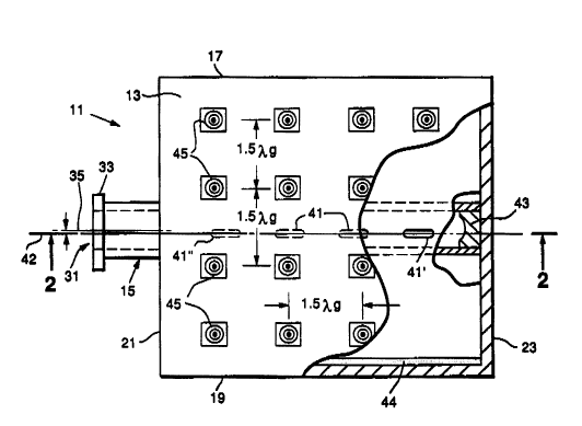
FIG. 2 is a bottom view of the flat cavity RF power divider shown in
FIG. 1.
FIG. 3 is a side elevational view of a flat cavity RF power divider
according to another embodiment of the present invention; and
FIG. 4 is a bottom view of the flat cavity RF power divider shown in
FIG. 3.
DETAILED DESCRIPTION
Referring now to the drawings, and more particularly to FIGS. 1 and 2,
there is shown a flat cavity RF power divider 11 having a flat cavity structure 13
and an input waveguide structure 15. The flat cavity structure 13 includes a
narrow upper longitudinal end wall 17, a parallel narrow lower longitudinal end
wall 19, a narrow left end wall 21, and a narrow right end wall 23. Also, this
structure has an inner broadwall 25, and an outer broadwall 27.
- 3b-
A
20668~
The input waveguide structure 15 is a WR-62 configuration and has an
input port 31 at an outer end of the structure 15 and is fitted with a conventional
waveguide flange 33. The waveguide further includes a waveguide centerline
35 and an inner waveguide wall 37 which is shared in common with the inner
broadwall 25 and is herein identified as common wall 39. As can be seen best
in FIG. 1, the waveguide centerline 35 is generally centrally disposed between
and parallel to the upper and lower longitudinal end walls (17 and 19) of the flat
cavity structure 13.
Four longitudinal coupling slots 41 are provided in the common wall 39
along a longitudinal slot centerline 42 which is offset from the waveguide
centerline 35 by 0.0089 inches at an operating frequency of about 14.35 GHz.
The slots 41 are sp~ced at 1.5 Ag, where ~9 is the WR-62 waveguide
wavelength. In this configuration, the longitudinal slots will not radiate if the
longitudinal slot centerline 42, along which the slots are disposed, coincides
with the waveguide~s inner broadwall. The 0.0089 inch offset locations is
optimized by empirical testing for this particular configuration.
A conventional curved waveguide short circuit structure 43, which is
broader in bandwidth than a regular straight edge short, is disposed at ~gt4
beyond the last slot 41' from the input port 31 to create a high standing-wave
along the WR~2 waveguide 15. Since the four slots 41 are spaced at multiples
of quarter wavelengths, a maximum E-field will occur to excite each slot. The
excited slot, in turn, excites its transverse axis column of the flat cavity depth
dimension, which in this case is 0.33 inches.
A virtual wall (E-field at zero, not shown) exists bel~//een each excited
slot column in the cavity 13. The virtual walls keep the RF pro~J~IJ~lio~ up or
down within the flat cavity very similar to a section of waveguide. However, a
virtual wall is not perfect like a real solid conductive wall and, thererore, higher
ordered modes do exist.
A technique to suppress these undesirable mode conditions is to place
a thin strip of conventional RF absorbing material 44 along the two longitudinalwalls of the flat cavity, namely, the upper longitudinal wall 17 and the lower
longitudinal wall 19. This technique increases the total insertion loss of the
power divider to -3dB, but is not sig"if,cant because there are conventional
simple RF amplifiers (not shown) that may be used to boost the gain of each
radiating element. These amplifiers incorporate conventional automatic gain
20668~
control (AGC) circuitry to overcome any uneven power levels vs. frequency
chalacteri~lics and output amplitude fluctuations between the output ports, as
will hereinafter be described.
In this embodiment, 16 output ports 45 are symmetrically distributed
across the outer broadwall 27 of the flat cavity structure 13. The output ports
45 each include conventional SMA probes with ~o/4 probe length penetrating
into the flat cavity to couple RF energy out. These ports are spaced 1.5 ~9
apart on the X, Y axes.
In accordance with a second embodiment of the present invention, as
shown in FIGS. 3 and 4, the symmetry feeding aspects of the invention have
been improved. Here, a flat cavity RF power divider 101 coi)".rises a flat cavity
structure 103 and an input waveguide structure 105. As best seen in FIG. 3,
the input waveguide 105 includes two major sections, a horizontal section 107,
and an orthogonally oriented input section 109. These two waveguide sections
join at a waveguide junction 111, having a conventional septum 111', centrally
disposed along the length of the horizontal section 107.
Curved waveguide short structures 113 (similar to structures 43) are
disposed at each end of the horizontal section 107. RF absorbing material 115,
similar to such material 45 in the first described embodiment, is disposed alongan upper longitudinal wall 117 and a lower longitudinal wall 119. As in the first
described embodiment of the invention, four longitudinal slots 121 lie along a
waveguide centerline 123 which is offset by 0.089 inches from a waveguide
section centerline 125 for the same reason as previously noted.
Input energy coupled to an input port 127 through input waveguide
flange 129 prop~g~tes inwardly along the input waveguide section 109 and is
split equally by the conventional tee junction 111, which energy is then
reflected back by each short 113 to excite their corresponding two longitudinal
slots 121 disposed in a common wall 131 between an inner broadwall 133 of
the flat cavity 103 and an inner broadwall 135 of the horizontal section 107 of
the input waveguide structure 105.
This design provides constant phase and amplitude distributions and
increased frequency bandwidth at the conventional SMA probes 137 provided
in an outer broadwall 139 of the flat cavity structure 103. Again, the probes are
spaced as previously noted, penetrating the flat cavity about ~o/4, and the slot
--5--
2 ~ 88 7
dimensions are about 0.175 inches by 0.395 inches. At an operating frequency
of 14.35 GHz, the internal flat cavity dimensions are 5.995 Ag by 5.805 Ag, witha width of 0.33 inches, and the inner width of the waveguides is 0.311 inches,
while the waveguide input port openings have a dimension of 0.311 by 0.622
inches. Further, an optimum thickness for the RF absorbing material 44 and
115 has been found to be about 0.080 inches.
From the foregoing it should be understood that there has been
described a new and improved flat cavity RF power divider and particularly a 1
to 16 flat cavity RF power divider that is very compact, light weight, emcient,
and that accommodates forced air cooling within the power divider. It is to be
understood that the above-described embodiment is merely illustrative of some
of the many specific embodiments which represent applications of the
principles of the present invention. Clearly, numerous other arrangements can
be readily devised by those skilled in the art without departing from the scope
of the invention.