Note: Descriptions are shown in the official language in which they were submitted.
YOg-9l-O9l 1 2~8001
HIGH DEFINITION MUI.TIMEDIA DISPLAY
FIELD OF THF INVENTION:
This invention relates generally to image display systems
and, in particular, to high resolution, multi-image
source display systems.
BACKGROUND OF THE INVENTION:
Contemporary supercomputer technology is often employed
for the visualization of large data sets and for
processing of real-time, high resolution images. This
requires large image data storage and control capability
coupled with the use of high resolution monitors, and
high resolution motion color images that are sampled in
real-time.
Many present-day supercomputers do not include a display
controller. A workstation which controls a user
interface with a supercomputer typically includes a
graphics controller, but can display only those images
generated within the workstation.
There is thus a need for a display controller separate
from a supercomputer and the controlling workstation for
visualizing and combining supercomputer output data,
and/or high definition television (HDTV) input, on a very
high resolution screen under a workstation user s
control.
Re~uirements for such a display controller include an
ability to process a variety of image or graphics
visuals, an ability to accommodate a variety of screen
resolutions, television standards, image sizes, and an
ability to provide color control and correction. By
example, the display controller should accommodate full
motion video real-time animated images, still images,
text and/or graphics. These images may be represented in
different formats, such as RGB, YUV, HVC, and color
YO9-91-091 2
~68001
indexed images. Different display resolutions may also
need to be accommodated, such as 1280 X 1024 pixels for
graphics image and 1920 X 1035 lines for HDTV. Finally,
there may be a requirement to show a stereoscopic image,
which consists of left and right views, that is shown at
twice the speed of a normal non-stereo, or planar, image.
One problem arises when a monitor is required to display
image data from a variety of sources, wherein the monitor
may have a resolution different from any of the image
data sources. Further comp]icating the display is a
requirement that diverse images be video refreshed
synchronously, and have a common final representation,
such as RGB.
Another problem is that visuals originate from different
sources, such as a television camera, a very high speed
supercomputer interface, and a slower interface with the
workstation host processor. It is clear that the
interfaces of the multimedia display to these sources,
and their data structures, are specific, but they must
also coexist. For example, providing maximum throughput
for a supercomputer data path must not interfere with a
television data stream, in that television images cannot
be delayed without losing information.
A further problem is tilat to overlay a plurality of
diverse images is a complicated process. Simple pixel
multiplexing becomes complicated in a multitasking
environment, where different images and their
combinations must be treated differently in different
application windows.
One possible solution to -these diverse problems is
derived from an approach used by a variety of known
multimedia display controllers. This solution treats
each image source separately and stores the data of each
source in a separate frame buffer. Each frame buffer may
have different dimensions, that is, resolution and number
of bits per pixel. All of the frame buffers are then
YO9-91-091 3
206g~Ql
refreshed synchronously. As can be realized, such a
system is expensive and requires a complicated, high
performance video data path, where all possible image
combinations must be handled. Although this conventional
approach may be referred to as "modular", it lacks the
integration required for a truly equal functional
treatment of all images from the user s point of view.
Furthermore, the amount of memory required to realize the
different frame buffers may be much larger than actually
needed to store the images. That is, due to fixed memory
chip organizations and capacities, and the diversity of
image representations and formats, an inefficient use of
memory may result, requiring more memory chips or modules
than that actually required to store a given image.
In commonly assigned U.S. Patent 4,994,912, issued
February 19, 1991, entitled "Audio Video Interactive
Display" to Lumelsky et al. there is described method and
apparatus for synchronizing two independent rasters such
that a standard TV video and a high resolution computer
generated graphics video may each be displayed on a high
resolution graphics monitor. This is achieved through
the use of dual frame buffers~ specifically a TV frame
buffer and a high resolution frame buffer. A switching
mechanism selects which of the TV video and the high
resolution graphics video is to be displayed at a given
time. The graphics data is combined with the TV video
for windowing purposes.
In commonly assigned U.S. Patent 4,823,286, issued April
18, 1989, entitled "Pixe] Data Path For High Performance
Raster Displays with All-Point-Addressable Frame Buffers"
to Lumelsky et al. there is described a multichannel data
path architecture which assists a host processor in
communicating with a frame buffer. Figures 12, 13, and
14 illustrate a plane mode, a slice mode, and a pixel
mode format which are rela-ted to the organization of the
addressing of the frame buffer.
YO9-91-091 4 206800~
In commonly assigned U.S. Patent 4,684,936, issued August
4, 1987, entitled "Displays Having Different Resolutions
For Alphanumeric and Graphics Data" to Brown et al. there
is described a display terminal that presents
alphanumeric and graphic data at different resolutions
simultaneously. The durations of the individual
alphanumeric and graphic dots have a fixed but
non-integral ratio to each other, and are mixed together
asynchronously to form a combined video signal to a CRT.
In U.S. Patent 4,947,257, issued August 7, 1990, entitled
"Raster Assembly Processo~" to Fernandez et al. there is
described a raster assembly processor that receives a
plurality of full motion video and still image input
signals and assembles these signals into a full bandwidth
color component, high resolution video output signal in
standard HDTV format (i.e. NHK-SMPTE 1125-line HDTV
format). A multi-media application is organized into a
plurality of overlapping windows, where each window may
comprise a video or a still image. A single multiported
memory system is utilized to assemble the multi-media
displays. Raster data is read out of the memory through
a multiplexer that combilles the signals present on a
plurality of memory output channels into an interlaced 30
frame/second HDTV signaL. A key based memory access
system is used to determine which pixels are written into
the memory at particular memory locations. Video and
still image signal pixels require four bytes,
specifically, Red (R), Green (G), and Blue (B) color
component values and a key byte, the key byte containing
a Z (depth) value. This patent does not address the
storage of a high definition video signal or the storing
and display of two real time images. Also, the provision
of a multi-resolution display output is not addressed.
Furthermore, the key data byte is employed for enabling
memory write operations ancl, as a result, after the video
is stored, the image within the window is fixed.
In U.S. Patent 4,761,642, issued August 2, 1988, entitled
"System For Providing Data Communication Between A
Y09-91-091 5 2~68001
Computer Terminal And A Plurality of Concurrent Processes
Running on a Multiple Process Computer" to Huntzinger
there is described a system that aLlows a single computer
to simultaneously run several processes and show the
output of each process in a correspondent display screen
window selected from a plurality of windows. Software
includes a screen process for maintaining a
subrectangular list comprising a set of instructions for
allocating window portions of the screen to the displays
defined by separate display lists.
In U.S. Patent 4,953,025, issued August 28, 1990,
entitled "Apparatus For Defining an Effective Picture
Area of a High Definition Video Signal When Displayed on
a Screen With A Different Aspect Ratio" to Saitoh et al.
there is described an apparatus for changing a video
input aspect ratio. Specifically, a HDTV video signal is
digitized, stored within a memory, and displayed on the
picture screen of an NTSC or other conventional
television monitor receiver having an aspect ratio that
differs from that of the HDTV format.
In U.S. Patent 4,631,588, issued December 23, 1986,
entitled "Apparatus and Its Method For The Simultaneous
Presentation of Computer Generated Graphics And
Television Video Signals" to Barnes et al. there is
described a method for generating a graphic overlay on a
standard video signal. The resulting video has the same
resolution and timing as the incoming video signal.
In U.S. Patent 3,904,817, issued September 9, 1975,
entitled "Serial-Scan Converter" to Hoffman et al. there
is described a scan-converter display for operating with
a variety of radar sweep signals or a variety of
television raster sweep sigllals. A serial main memory is
used for refreshing the display at a rate much higher
than a radar data acquisition rate. A sweep format of a
common display is altered so as to accommodate video from
a variety of sources of different video formats.
- YO9-9l-09l -2068001
What is not taught by these patents, and what is thus one
object of the invention to provide, is a multimedia
display for storing and displaying a plurality of real
time images, and which furthermore enables the use of a
plurality of programmable output video resolutions.
It is another object of the invention to provide a novel
frame buffer organization so as to achieve an efficient
use of memory devices.
It is a further object of the invention to provide for
the display of image data from a plurality of image
sources, including a plurality of real time image
sources, with a single frame buffer.
It is another object of the invention to provide a video
image storage format wherein a pixel includes R, G, B
data and associated key data, the key data being used for
controlling an output video data path and enabling the
display of stored video images to be altered.
SUMMARY OF THE INVENTION
The foregoing and other problems are overcome and the
objects of the invention are realized by image display
apparatus that includes an image buffer having a
plurality of addressable locations for storing image
pixel data and circuitry, having an input coupled to an
output of the image buffer, for converting image pixel
data read therefrom to electricaL signals for driving an
image display. The circuitry is responsive to signals
generated by an image display controller for generating
one of a plurality of different timing formats for the
electrical signals for driving an image display having a
specified display resolution. The apparatus further
includes circuitry, responsive to signals generated by
the image display controller, for configuring the image
buffer in accordance with the specified display
resolution.
Y09-91-091 7 2Q680~1
The image buffer is confi.gurable, by example, as two,
2048 location by 1024 location by 24-bit buffers and one
2048 location by 1024 location by 16-bit buffer; or as
two, 2048 location by 2048 location by 24-bit buffers and
one 2048 location by 2048 location by 16-bit buffer; or
as four, 2048 location by ]024 location by 24-bit buffers
and two 2048 location by 1024 location by 16-bit buffers.
Each of the 24-bit buffers store R,G,B pixel data and the
16-bit buffers each store a color index (CI) value and an
associated window identifier (WID) value received from
the image display controller. Circuitry at the output of
the image buffer decodes a CI value and an associated WID
value to provide R,G,B pixel data.
The apparatus further includes a first interface having
an input for receiving image pixel data expressed in a
first format and an output coupled to the image buffer
for storing the received image pixel data in a R,G,B
format. The first interface may be coupled, by example,
to a supercomputer for receiving 24-bit R,G,B image pixel
data therefrom.
The apparatus furtller includes a second interface having
an input for receiving image pixe] data expressed in a
second format and an output coupled to the image buffer
means for storing the received image pixel data in a
R,G,B format. The second interface is coupled to a source
of HDTV image data and includes circuitry for sampling
the HDTV analog signals and for converting the analog
signals to 24-bit R,G,B dat:a.
A third interface is coupled to the image display
controller, specifically the data bus thereof, for
receiving image pixel data expressed in the CI and WID
format.
The CI value and the associated WID value are decoded,
after being read from the image buffer, to provide a key
signal specifying, for an associated image pixel, a
contribution of the R,G~B data from the first interface,
"
~ YO9-91-091 8 20~8001
a contribution of the R,G,B data from the second
interface, and a contribution of the R,G,B, data decoded
from the CI and WID values.
BRIEF DESCRIPTION OF THE DRAWING
The above set forth and other features of the invention
are made more apparent in the ensuing Detailed
Description of the Invention when read in conjunction
with the attached Drawing, wherein:
Fig. 1 is a block diagram of an image display system that
includes a High Definition Multimedia Display (HDMD);
Fig. 2 is an overall block diagram of the HDMD showing
major functional blocks thereof;
Fig. 3 is a block diagram showing one of the frame
buffers (FB);
Fig. 4 depicts a memory architecture of each FB
configured as a single block of 2K X 2K X 32 bits and
organized in a three-dimensional 4 X 2 array of VRAMs;
Fig. 5a, shows the FB organized as two, 16 VRAM slices,
vertically oriented in the drawing;
Fig. 5b depicts a workstation display line order;
Fig. 6a illustrates the VRAM secondary port data bits
SDQ;
Fig. 6b illustrates four of the buses that serve as 8-bit
FB color components; --
Fig. 6c il]ustrates FB control sigllals and primary port
data;
Figs. 7a and 7b illustrate the FB with A and B buffers
split horizontally;
YO9-91-091 9
2Q680Ql
Fig. 8 illustrates the organization of a dual FB, high
resolution embodiment;
Fig. 9 illustrates, for the high resolution case, a pixel
horizontal distribution where all even pixels are stored
in a first FB, and all odd pixels are stored in a second
FB;
Fig. lOa shows two HDTV fields and the scan line
numbering of each;
Fig. lOb illustrates a HDTV image line distribution;
Fig. 11 is a block diagram of one of four workstation
data path devices employed at an output of each FB;
Fig. 12a is a block diagram of a FB controller;
Fig. 12b is an illustrative timing diagram of a
synchronous transfer of three data bursts from a source
(S) to a destination (D) over a High Performance Parallel
Interface (HPPI);
Fig. 12c illustrates an adaptation made by the system of
the invention to the HPPI data format of Fig. 12b;
Fig. 12d illustrates in gr-eater detai] the organization
of the Image Header of Fig. 12~;
Fig. 12e shows two state machines and their respective
inputs and outputs.
Fig. 13 is a timing diagram illustrating the operation of
A/B Buffer selection logic of the FB controller;
Fig. 14 illustrates eight serial data paths, four of
which serve FBA and fo~lr which provide a serial data path
for the FBB;
YOg-9l-O9l lO 206~001
Fig. 16 illustrates the VDPR device employing eight
groups of two multiplexers;
Fig. 17 illustrates the VIDB 24 includes three DAC s
(24cl, 24c3, 24c3) each having a 2:1 multiplexer at the
inputs;
Fig. 18 is a timing diagram that depicts medium
resolution horizontal and vertical synchronization
pulses;
Fig. 19 illustrates two counters of a timing
synchronization generator, one for an x-axis direction
and one for a y-axis direction;
Eig. 20 illustrates the inputs, outputs, and the
functional blocks of a high speed interface; and
Fig. 21 illustrates a HDTV interface which provides
digitization of a full color, full motion HDTV image in
real time; and buffers this data for transfer to the FB
and to the HSI.
DETAILED DESCRIPTION OF THE INVENTION
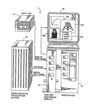
Referring to Fig. 1 there is shown an illustrative
embodiment of the invention. A High Definition
Multimedia Display contro]ler (HDMD) 10 receives image
data from a supercomputer visualization system (SVS) 12,
a HDTV source 14, and a workstatioll 16, and sends sampled
HDTV image back to a supercomputer via the SVS 10. The
HDMD 10 also serves display monitors 18, which may be
provided with differing resolutions. As employed herein,
a medium resolution monitor is considered to have, by
example, 1280 pixels by 1024 pixe]s. A high resolution
monitor is considered to have, by example 1920 pixels by
1536 pixels or 2048 pixels by 1536 pixels. HDTV
resolution is considered to be 1920 pixels by 1035
pixels. An example of the screen content of monitor 18
shows a supercompu-ter synthesized image 18a, a HDTV image
~ Y09-91-091 11 2~0Ql
18b, and user interface (workstation) images 18c each in
a different, overlapping window. The workstation 16 may
or may not include its own monitor, depending on the
user s preference, in that the user interface may run
directly on the HDMD monitor 18. The workstation 16
interface may be a plug-in board in the workstation 16,
which provides the required electrical interface to the
HDMD 10. In a preferred embodiment this interface
conforms to one known as Microchannel. In general, any
workstation or personal computer may be used for a user
interface with a suitable HDMD 10 interface circuit
installed within the workstation. As such, the circuitry
of the HDMD 10 functions as an addressable extension of
the workstation 16.
By way of introduction, the HDMD 10 includes the
following features, the implementation of which will be
described in detail below.
The HDMD 10 Frame Buffer architecture is reconfigurable
to accommodate different user requirements and
applications. These include a requirement to provide
very high resolution, full color supercomputer images,
such as 2048 pixels by 1536 pixels by 24-bits, doubled
buffered; a requirement to support both supercomputer and
HDTV full color images, with a full speed background
overlay through the use of two, 2048 pixel by 1024 pixel
buffers (one double buffered); a requirement to provide
only HDTV or only supercomputer medium resolution image
display with graphics overlay with 2048 pixel by 1024
pixel by 24-bits (double buffered) and 2048 pixel by 1024
pixel by 16-bit graphics from the workstation; a
requirement to provide an i.nterlaced HDTV input and a
very high resolution, non-interlaced output; and a
requirement to support a stereoscopic (3-dimensional
image) output.
An open-ended architecture approach enables expansion of
a HDMD frame buffer to satisfy appropriate image storage
and input and output bandwidth requirements, without
~ Y09-91-091 12 2~8U~l
functional changes. As a result, the user may define
monitors with different screen resolutions, different
frame sizes, format ratios, and refresh rates.
The user may also preprogram video synchronization
hardware in order to use different monitors or projectors
and accommodate future television standards and various
communication links.
The architecture also provides simultaneous display of
full color, real-time sampled HDTV data and SVS processed
video data on the same monitor. To this end the HDMD 10
provides synchronization of a fast supercomputer image
with the local monitor 18 attached to the frame buffer,
thus eliminating motion artifacts due to variable frame
rates of data received from a supercomputer.
The HDMD 10 also provides sampling and display of HDTV
video. Reprogrammable synchronization and control
circuitry enables different HDTV standards to be
accommodated.
The HDMD 10 also provides a digita]. output of sampled
HDTV data to an external device, such as a supercomputer,
for further processiny. A presently preferred
communication link is implemented with an ANSI-standard
High Performance Parallel Interface (HPPI).
The HDMD lO also supports multitasking environments,
allowing the user to run several simultaneous
applications.
By example the user may define application windows and
the treatment of internal and external images in the
defined windows. The user also controls HDTV image
windowing and optional hardware scaling.
The HDMD 10 memory architecture furthermore accommodates
very high density video RAM (VRAM) devices, thereby
reducing component count and power consumption.
-- YO9-91-091 13 2~680Ql
.,
Referring now to Fig. 2 there is shown an overall block
diagram of the H~MD 10. The HDMD 10 includes six major
functional blocks. Five of the blocks are implemented as
circuit boards that plug into a planar. The major blocks
include two Frame Buffers memories (FBA) 20 and (FBB) 22,
a video output board (VIDB) 24, a high speed interface
board (HSI) 26, and a high definition television
interface (HDTVI) 28. One FB and the VIDB 24 are
required for operation. All other plug-in boards are
optional and may or may not be installed, depending on
the system configuration defined by a user.
A Workstation Data Path (WSDP) device A 30 and B 32, a
Serial Data Path device 34, a Video Data Path device 36,
a workstation (WS) interface device 38, two Frame Buffer
controllers FBA CNTR 40 and FBB CNTR 42, and two state
machines SMA 44 and SMB 46, are physically located on the
planar and fulfill common display control and data path
functions.
The HSI 26 provides an interface with the SVS 12 and
passes SVS 12 images directly to the FBA 20 and/or FBB
22. The HSI 26 also receives sampled video data from the
HDTVI 28 and passes the sampled data to the SVS 12 for
further processing.
The FBA 20 and FBB 22 are implemented using dual port
VRAMs of a type known in the art. A primary port of each
FB receives data from the SVS 12 or the HDTVI 28, via
multiplexers 48 and 50, or data from WSDPA 30 or WSDPB
32. A secondary port of each FB shifts out four pixels
in parallel to the Serial Data Path 34. The shift-out
clock is received from a VIDB 24 synchronization
generator (SYNCGEN) 24a ancl is programmable, depending on
a required screen reso]ution, up to a 33 MHz maximum
frequency. Thus, one FB provides up to a 132 MHz (4
pixels x 33 MHz) video output, and two FBs provide up to
a 264 MHz (8 pixels x 33 MHz) output. The latter
frequency corresponds to a 3 X 106 pixel, 60 Hz,
non-interlaced video output.
-~ Y09-91-091 14 2~0Ql
The Serial Data Path 34 combines the FBA 20 and FBB 22
serial outputs; representing a 24-bit red, green, and
blue (RGB) SVS image, a ]6-bit color WS 16 image, and
multiwindow control codes. The Video Data Path 36
implements multiwindow control functions for image
overlay. The output of the Video Data Path 36 provides
R, G, B digital data for four or eight pixels in
parallel, and passes the plxel data to the VIDB 24
serializers 24b.
A primary function of the VIDB 24 is to display images
stored in one or both FBs 20, 22. The serialized digital
outputs of the Video Data Path 36 are applied to high
performance DAC s 24c for conversion to analog red, green
and blue monitor 18 inputs. In addition, VIDB 24
provides video synchronization to the secondary ports of
the FBs 20, 22. The SYNCGEN block 24b supplies a video
clock to the DACs 24c, and video and memory refresh
requests to the state machines SMA 44 and SMB 46.
The HDTVI 28 fullctions as a HDTV video digitizer and
scaler and as a source of image data for one or both FBs
20, 22. In addition, it reformats its digital video
output to be transmitted back to the SVS 12 through a
HPPI output port of the HSI 26.
The FBA 20 and FBB 22 are controlled by the FBA CNTR 40
and FBB CNTR 42, respectively, and the state machines SMA
44 and SMB 46, respectively. The state machines generate
signals to execute memory cycles and also provide
arbitration between HPPI, SYNCGEN 24a, and WSDP 30, 32
bus requests. If both HDTV and SVS image sources are
used, the state machines work independently. If
HDTV-only or SVS-only sources are used, the state machine
SMA 44 controls both FBs 20, 22 in parallel, via
multiplexer MUX 52.
The FBA CNTR 40 and FBB CNTR 42 provide all addresses and
most memory control signals for the FBs 20, 22. Each
receives timing control from the SYNCGEN 24a and SVS and
. YO9-91-091 15 2~6~00~
HDTV image window coordinates from the HSI 26 and HDTVI
28, respectively.
The WS interface 38 provides the user with access to all
control hardware, and to the Frame Buffers 20, 22. It
also provides a signal to SMA 44 and SMB 46 indicating a
workstation request.
As illustrated in Fig. 2, there are two multiplexors in
the data path. Multiplexor M[IXl 48 allows an incoming
image from the HSI 26 to be written in both FBs 20, 22.
Multiplexor MUX2 50 allows HDTV images to be written in
both FBs 20, 22. The former mode of operation enables a
supercomputer image to be displayed on a high resolution
monitor, and the latter mode of operation enables a HDTV
image to be displayed on a high resolution, noninterlaced
monitor. A third mode enables an output of a medium
resolution image in a stereoscopic 3D mode. In this
third mode, the image is treated as a high resolution
image, and is written to both FBA 20 and FBA 22. The
data from both FBs is sent to the serial data path 34
with a vertical frequency of 120 Hz, and with a 240 MHz
video pixel clock. The same approach may be employed to
display a stereoscopic HDTV image rendered by an external
data processor, such as a s-lpercomputer.
Based on the foregoing, possib]e configurations and
applications of the HDMD lO include the following.
The HDMD 10 may be operated in a medium resolution
output, SVS-only input mode. One FB and the HSI 26 are
required. Applications include supercomputer-only
graphics on a medium resolution or a HDTV standard
display monitor. For example, images may be displayed
and modified on a non-interlaced medium resolution
screen, and stored frame by frame on a supercomputer disk
array. The stored image may then be read back from the
supercomputer disk array to the FB, displayed by the VIDB
24 operating in HDTV mode. and recorded on a HDTV tape
Y09-91-091 16
recorder in real time, e.g. 30 frames/sec., thus
providing smooth motion video.
The HDMD 10 may also be operated in a high resolution
OUtptlt, SVS-only input mode. Both the FBA 20 and the FBB
22 and the HSI 26 are required. The input HPPI data is
written to both FBs 20 and 22. In this mode of operation
the HDMD 10 is used for supercomputer--only graphics and
high resolution imaging.
The HDMD 10 may also be operated in a medium resolution,
SVS and HDTV input mode. Both FBS 20 and FBB 22, the HSI
26, and the HDTVI 28 are required. Sampled HDTV frames
are sent fully or partially back to the supercomputer
through HSI 26, and also to the monitor 18 through the
FBB 22. The image, as processed by the supercomputer, is
sent back to the FBA 20 for storage. Both images thus
coexist in separate or overlapping windows on the same
monitor 18, providing convenient access to both an
unprocessed and a processed video source.
The HDMD 10 may also be operated in a high resolution
output, HDTV-only input mode. Both the FBA 20 and the
FBB 22, and the HDTVI 28 are required. An interlaced HDTV
image is shown on a very high resolution monitor 18
operating in a non-interlaced mode. An advantage of this
mode of operation is that the very high resolution
monitor 18 provides 30 per cent more screen area than the
HDTV resolution requires. This additional screen area
may be used for user interface text or graphics from WS
16.
The HDMD 10 may also be operated in a stereoscopic output
mode. Both the FBA 20 and the FBB 22, and the HSI 26 or
the HDTVI 28 are required to display either a medium
resolution or HDTV stereoscopic image. Both FBs 20 and
22 are required in order t-o double the video bandwidth,
providing a wider serial data path. Hence, in the
stereoscopic mode, one half of the available FB memory is
not used for image storage.
YO9-91-091 17
20~8~01
Having described the general construction of the HDMD 10,
and having provided severaL examples of its use, each of
the functional blocks of Fig. 2 is now described in
further detail.
_ FBA 20, FBB 22
,,,
Fig. 3 depicts the FBA 20, it heing realized that the FBB
22 is identically constructed. The FBA 20 stores 128
Mbits (128 x 106 bits) of data and includes 32, 4-Mbit
VRAM devices 20a. Each VRAM 20a is organized as 256K
words by 16-bits per word. The I/O pins of the VRAMs 20a
are connected vertically, providing four, 32-bit data
paths DQO-DQ3. The lower 24 bits of these data paths are
coupled to one of four pipeline registers RO-R3, which in
turn are loaded from a 64-bit SVSA bus by four clock
pulse sequences RCLKO-RCLK3. Each of the 32-bits of each
data path DQO-DQ3 is also coupled to one of four
bi-directional workstation data path devices 30
(WSDPO-WSDP3).
As was noted previously, the supercomputer image employs
a dual buffer FB for storing two 24-bit data words for
each screen location. Also, the WS 16 image requires
16-bits per pixel, where 8-bits are a color index (CI)
value (converted further to 24 bits using video look-up
tables), and 8-bits represent a pixel attribute, or
display screen window identification (WID) number. The
dual FB mode is not required for the WS 16 data, since WS
performance is generally too low to deliver motion
images.
In accordance with a convention used herein, the VRAMS
20a are designated FBxmni. where x=A for FBA 20, x = B
for FBB 22, m is a row number equal to 0, 1, 2, or 3, n
is a column number equal to 0, 1, 2, or 3, and i is a
VRAM number in the z-direction (front = O and back = 1).
Thus, FBxOni refers to the eight VRAMs in the upper row
of either frame buffer. FBxmOi refers to the eight VRAMs
in the left-most column of either frame buffer; FBAmO
YOg-9l-O9l la ~6~0Ql
refers specifically to the 8 VRAMs in the left-most
column of FBA 20; and FBB231 refers to the VRAM located
in FBB 22, the second row, third column, in a rear
"slice".
The organization shown in Fig. 4 substantially reduces
the data and video path bit-width. In addition, it
minimizes the number of control signals. It should be
realized that such a FB may also be used as a 2K X 2K X
32 bit general purpose memory.
However, in accordance with an object of the invention,
there is provided a Frame Bu~fer that is configured as
two, 2048 location by 1024 location by 24-bit buffers and
one 2048 location by 1024 location by 16-bit buffer; or
as two, 2048 location by 2048 location by 24-bit buffers
and one 2048 location by 2048 location by 16-bit buffer;
or as four, 2048 location by 1024 location by 24-bit
buffers and two 2048 location by 1024 location by 16-bit
buffers; wherein the 24-bit buffers store R,G,B pixel
data and the 16-bit buffers store the CI and the WID
data.
Referring to Fig. 3 and Fig. 5a, it can be seen that the
FBA 20 may be considered as having two, 16 VRAM slices,
vertically oriented in the drawing. The front slice has
I/O pins numbered as (0:16) and stores the lower 16-bits
of the 24-bit SVS image. The rear slice is represented
by two portions. One portion has I/O pins numbered as
(17:23), and stores the upper 8-bits of the 24-bit SVS
image. The second portion of the rear slice is shown in
separately in Fig. 5b and stores the 16-bit WS 16 image
data as 8-bits of CI and 8-bits of WID for each WS 16
pixel.
.
As was said previously, for the medium resolution case
the SVS image is stored as a 2K X lK double-buffered
image. If two buffers, not to be confused with the Frame
Buffer A 20 and the Frame Buf~er B 22, are designated as
buffers A' and B , then the SVS image is stored as shown
Yog-gl-O9l 19 2Q68~Ql
in Fig. 5a, where lines O, 1, 2, 3 of buffer A have a
row address of O in all VRAMs, and are stored in the FBO,
FBl, FB2, FB3 slices, respectively, while lines O, 1, 2,
3 of buffer B have a row address of 256 in all VRAMs,
and are stored in the FB2, FB3~ FBO, FBl slices,
respectively. Lines 5, 6, 7, 8 have row addresses
incremented by one relative to lines O, l, 2, 3, etc.
The WS 16 line order is shown in Fig. 5b. Line O of the
color index (CI) data (bits (0:7) of the WS image pixels
is stored in the upper row of VRAMs having memory row
address O. Line O of the window identification number
(WID) (bits (8:15) of the WS image pixels) is stored in
the third row of VRAMs with row address 256. Line l of
CI data is stored in the second row with memory row
address O, and line 1 of WID data is stored in the fourth
row of VRAMs with memory row address 256, etc. Line 5
data is stored in the same rows of the VRAMs with memory
row addresses incremented by four relative to line O,
etc.
This novel line/address distribution technique provides a
reduction in a required width of the Serial Data Path 34.
This technique of image line distribution also permits
the majority of VRAM serial input/output bits to be
connected and thus significantly improves the efficiency
of VRAM utilization. A totaL of 16 conductors in each
column are multiplexed by means of eight, 2-to-1
multiplexors 54. As a result, each column's serial
output supplies 40 bits of R, G, B, CI and WID data.
To further explain the organization of the serial output,
Fig. 6a illustrates the VRAM secondary port output data
bits SDQ, and specifically shows the SDQ connections for
the eight VRAMs in column n . The FBmnO VRAMs have SDQ
connected bit-wise, providing a 16 wire serial output.
Connected are SDQ bits (7:0) for FBxOnl and FBxlnl, bits
(7:0) for FBx2nl and FBx3nl, bits (15:8) for FBxOnl and
FBxlnl, and bits (15:8) for FBx2nl and FBx3nl. There are
thus a total of six, 8-bit serial data buses. As seen in
YO9-91-091 20 2 Q r~ IQ ~ ~ ~
Fig. 6b four of the buses serve as 8-bit FB color
components: SVSBn<7:0> for blue, SVSGn<7:0> for green,
and SVSRAn<7:0> and SVSRBn<7:0~ for the red color. The
red bits are multiplexed based on two bits of a video
refresh address, providing the SVS Red component. The
multiplexer 54 (Fig. 5b) eliminates serial bus contention
in that, for every video line, the serial outputs of two
rows of the FB chips are enabled to provide the WID and
CI outputs of the WS image. As a result, the red portion
of the 24-bit SVS image is enabled simultaneously for two
lines, since the red information is stored in the same FB
portion as CI and WID.
However, high resolution images require a different line
placement than that jus-t described for the medium
resolution case. The SVS image is stored in dual, 2K X
2K X 24-bit buffers. The im~ge buffer organization is
illustrated in Fig. 7a and 7b, where the SVS line
distribution (Fig. 7a) is similar to that of the medium
resolution case, but the A and B buffers are split
horizontally. In other words, lines in buffers A and B
differ not by row address, but by column address.
Workstation 16 lines are distributed accordingly, as seen
in Fig. 7b.
Fig. 8 illustrates the organi~ation of the dual frame
buffer, high resolution case. In Fig. 8 it can be seen
that the two frame buffers (FBA 20 and FBB 22) each
contain elements of the dual (A , B ) SVS 2K X 2K X
24-bit buffers, and that the WS 16 image buffer also
split between the two FBs.
For the high resolution case, the pixel horizontal
distribution is illustrated in Fig. 9, where all even
pixels are stored in FBA 20, and all odd pixels are in
FBB 22. This organization causes the output of the Serial
Data Path 34 to be more uniformly distributed at the
input to the Video Data Path 36.
YO9-91-091 21
2~680Ql
Fig. lOa shows two HDTV fields with the scan line
numbering of each. The HDTV image line distribution is
~hown in Fig. lOb. It resembles the medium resolution
frame buffer organization described previously, but
because the number of visible HDTV lines is equal to
1035, the first 1024 lines are stored in buffer A , and
the remainder are stored in buffer B , in the order
shown.
Various FB memory cycles, including workstation
read/write operations, video refresh cycles, etc., are
initiated by the FBA CNTR 40 and FBB CNTR 42 devices. The
FB CNTRs provide VRAM control signals, as seen in Fig. 3
and in Fig. 6c, and FB addresses (not shown, but common
to all VRAMs). Each row of the FBs (FBxOmi, FBxlmi;
FBx2mi, and FBx3mi) has a corresponding row address
strobe (RAS) signal (RASO-RAS3, respectively), while each
column (FBxnOi; FBxnli, FBxn2i, and FBXn3i) has a
corresponding column address strobe (CAS) signal
(CASO-CAS3, respectively). There are four write enable
(WE) signals WEWS, WER, WEG, and WEB, one for each 8-bits
of the 32-bit FB, which allow writing to individual
bytes. The serial enable signals (SE<0:3>) specify a
line number to be video refreshed. That is, the two
least significant bits of the video refresh address
enable one of the SE signals. The SE <0:3> signals
control only the FBxmnO VRAMS, for only one row of these
VRAMs are required for each particular line. In
contrast, the FBxmnl VRAMs store not only the red image,
but also the WS image, which is stored in two memory
rows. Therefore, two additional serial enable signals SE
4,5 are generated by OR gates ORl and OR2 for the FBxmnl
VRAMs. These aspects of the invention are also described
in greater detail below in relation to Fig. 12a.
Workstation Data Path 30,32
As seen in Fig. 3 the data path from the WS 16 to the FB
enables WSDP A 30 or WSDP B 32 data to be written to or
read back from the FBs. The WSDP architecture enables
YO9-91-091 22
2~00~
one 32-bit workstation word to represent different
operations, depending on a user-specified MODE. For
example, a workstation word may represent four, 8-bit
workstation Color Index or WID va]ues, or one 24-bit
full-color pixel, or a single 8-bit color component for
each of four successive pixels. This degree of
flexibility is achieved by using four WSDPs, where the WS
16 data is common to all four~WSPPs and where each has a
separate 32-bit output to the associated FB.
A block diagram of one of the four WSDP 30 or 32 devices
is shown in Fig. 11. The input WS 16 data is shown as
partitioned into four bytes at the bottom, while the four
FB output bytes are shown at the top. There are four
subsections, of two different types, denoted DPBLKl and
DPBLK2. DPBLKl is used in only the leftmost subsection.
The subsections in the other WSDP devices are
functionally identical to DPBLKl and DPBLK2, where the
DPBLKl block moves one section to the right for each of
the three other WSDP devices. For example, in WDSP 3,
DPBLKl is the right-most subsection, which connects
WSDB(7:0) with DQ3(7-0), where DQ3 refers to the
rightmost 32-bit FB data bus. Output buffers (OB0-OB3)
are enabled through BE decoder 54 by a decode of a memory
operation code ~MOP) from the associated SMA 44 or SMB
46, when MOP is decoded as a Workstation Write (MOPWSWT)
operation.
FB writing occurs as either color plane (PLANE mode)
writes or pixel (PEL mode) writes. The mode is defined
by a PLANE/PEL signal generated by the associated FBA
CNTR 40 or FBB CNTR 42. For PLANE mode writes, which
include four 8-bit members of a set (e.g. 4 Red, 4 Green,
4 WS Color Index, etc.), one byte of the WSDB drives all
four DQ bytes on the output to the FB. In Fig. 11, WSDB
(31:24) passes through DPBI,Kl to drive DQ0(31:24). It is
also selected by the 2-to-1 multiplexer MUXl 56 in each
DPBLK 2 block to drive the three bytes of DQ(23:0). In
the WSDP(l) WSDB(23:16) drives~all 32-bits of the FB data
path DQl(31:0), and so forth in WSDP(2) and WSDP(3). The
_ .,
YO9-91-091 23
~'g~)Ql
Write Enable signals (WER, WEG, WEB, and WEWS), are
employed to select which component of the FB is written.
For example, to write four Red pixels the four red values
are presented on WSDB(31:0). WSDB(31:24) drives
DQ0(31:0), WSDB(23:16) drives DQ1(31:0), WSDB(15:8~
drives D02(31:0), and WSDB(7:0) drives DQ3(31:0). The
signal Write Enable Red (WER) is a~tivated, and the Red
components are driven to each of the four EB DQ buses,
with the result that four 8-bit Red components are
written within the FB with one 32-bit WS 16 write.
Pixel mode writes operate as follows. All four WSDPs
couple the 32-bit WSDB bus directly to their respective
32-bit FB DQ data buses. One column of the FB i5 written
by activation of that column s CAS signal. Hence, one
24-bit (or 32-bit, if appropriate) pixel value is written
to the FB in a 32-bit WS 16 write.
;
Workstation Read cycles ope~ate similarly, with the
appropriate data steering being provided by selectively
enabling the 8-bit drivers on the WS 16 side of the WSDP
devices, via the Byte Enable signals (BE0:3) generated by
the decoder BE DECODE 54.
For a FB data read in PLANE mode, each WSDP device is
enabled to drive one of the four WSDB bytes. WSDP(0)
drives WSDB(31:24), WSDP 1 drives WSDB(23:15), etc. The
selection of which component (R, G, WS, etc.) to read is
made by a 4-1 multiplexer (MUX) 58. The MUX 58 control
signals PSEL0 and PSELl are generated by the BE DECODE 54
by decoding WSADDR. For example, to read the Red
component, PSEL (1:0) is set to "01" and four Red pixel
components on DQx(23:16) (x=0 to 3) are transferred to
the WSDB.
For pixel mode reads, only one of the four WSDP devices
drives WSDB, depending on the address of the pixel being
read. When 32-bit pixel values are used, all 4 bytes are
driven. Otherwise, for 24-bit pixel values only WSDB
(23:0) are driven.
~ :
~ ~ '
YO9-91 -091 24
Two other functions included in the WSDP devices are a Plane Mask and aBlock Write feature. The Plane Mask enables selective bits of the 24-bit RBG
or 8-bit WS pixels to be protected from writes via a conventional ~,vrite-per-bit
function of the VRAMs. The Block Write feature enables a performance gain by
exploiting another feature of the VRA~S. A static color is first loaded into theVRAMs using a "Color Write" cycle. Then, a 32-bit word from the WS 16 is
reinterpreted as a bit mask, where pixels with corresponding l's are set to the
stored color, while those with 0's are not written. This feature is especially useful
for text operations, where a binary font may be directly used to provide the mask.
In order to use this feature, the 32-bits of WS data are rearranged via logic
provided in the WSDP devices.
FBA CNTR 40 and FBB CNTR 42
Fig. 12a is a block diagram of one of the FB CNTRs 40 or 42. The FB CNTR
provides all of the addresses and most of the control signals to the associated FB .
The FB CNTR includes: counters 60 and 62 to automatically address rect~ng~ r
regions of the FB as pixel data arrives from the HSI 26, HDTVI 28, or WS
Interface 38; a video refresh (VREF) counter 64; a WS Address Translator 66;
write-enable (WE) Generation logic 68; RAS and CAS Generation logic (70, 72),
address multipliers 74a, 74b, 74c; and A/B Logic 76 to synchronize incoming
double buffered SVS data with the monitor 18. The FB CNTR also contains a
MODE register 78 that determines a type of access performed by the WS 16.
As will be made apparent below, one feature of the invention is the loading of
HPPI data into the FBs. In this regard reference is made to commonly assigned
Canadian Patent Application No. 2,067,471, filed April 28, 1992, entitled
"Communication Apparatus and Method for Transferring Image Data From A
Source To One Or More Receivers", S. Choi et al.
l ~
~ ~ :
YO9-91-091 25
Referring to Fig 12b there is shown an illustrative timing diagram of asynchronous transfer of three data bursts from a source (S) to a destination (D)in accordance with the HPPI specification entitled "High-Performance Parallel
Interface Mechanical, Electrical, and Signalling Protocol Specification (HPPI-
PH)" preliminary draft proposed, American National Standard for Information
Systems, November 1, 1989, X3T9/88-127, X3T9.3/88-032, REV 6.9.
Each data burst has associated therewith a length/longitudinal redundancy
checkword (LLRC) that is sent from the source to the destination on a 32-bit
data bus during a first clock period following a data burst. Packets of data bursts
are delimited by a PACKET signal being true. The BURST signa} is a delimiter
marking a group of words on the HPPI data bus as a burst. The BURST signal
is asserted by the source with the first~ word of the burst and is deasserted with
final word. Each burst may contain from one to 256 32-bit data words. A
REQUEST signal is asserted by the source to notify the destination that a
connection is desired. The CONNECT signal is asserted by the destination in
response to a REQUEST. One or more READY indications are sent by the
destination after a connection is established, that is, after CONNECT is asserted.
The destination sends one ready indication for each burst that it is prepared toaccept from the source. A plurality of READY indications may be sent from the
destination to the source to indicate a number of bursts that the destination isready to receive. For each READY indication received, the source has
permission to send one burst. Not shown in Fig. 12b is a CLOCK signal defined
to be a symmetrical signal having a period of 40 nanoseconds (25MHz) which is
~m~ yed to synchronously time the transmission of data words and the various
control signals.
In summary, the HPPI-PH specification defines a hierarchy for data transfers,
where a data transfer is composed of
YO9-91-091 2q
2 ~ Q l
one or more data packets. Each packet is composed of one
or more data bursts. Bursts are composed of not more
than 256 32-bit data words,~ clocked at 25MHz. Error
detection is performed across a data word using odd
parity on a byte basis. Error detection is performed
longitudinally, along a bit column in the burst, using
even parity, and is then appended to the end of the
burst. Bursts are transmitted on the ability of a
receiver to store or otherwise absorb a complete burst.
The receiver notifies the transmitter of its ability to
receive a burst by issuing the Ready signal. The HPPI-PH
specification allows the HPPI-PH transmitter to queue up
63 Ready signals received from a receiver.
Fig. 12c illustrates an adaptation made by the system of
the invention to the HPPI data format of Fig. 12b to
accomplish image data transfer~. A packet of data bursts
corresponds to either a complete image frame, or to a
rectangular subsection thereof, referred to as a window.
The packet includes two or more bursts. A first burst is
defined to be a Header burst and contains generic HPPI
device information, the HPPI Header, and also image data
information, referred to herein as an Image Header. The
remainder of the Header burst is presently unused.
Following the Header burst are image data bursts
containing pixel data. Pixel cata is organized in raster
format, that is the left-mos pixel of a top display
scanline is the first word of the first data burst. This
ordering continues until the last pixel of the last
scanline. The last burst is padded, if required, to full
size. Each data word contains 8-bits of red, 8-bits of
green, and 8-bits of blue (RGB) color information for a
specific pixel The remaininy 8-bits of each 32-bit data
word may be employed in several manners. For linear the
mixing two images, the additional 8-bits may be used to
convey key, or alpha, data for determining the
contribution of each input image to a resulting output
image. Another use of a portion of the additional 8-bits
of each data word is to assign two additional bits to
YO9-91-091 27
2Q~OOl
each color for specifying 10-bits of RGB data. Also, a
number of data packing techni~ues may be employed wherein
the additional 8-bits of each word are used to increase
the effective HPPI image transfer bandwidth by one third,
when using 24-bit/pixel images.
! Fig- 12d illustrates in greater detail the organization
of the Image Header of Fig. 12c. A HPPI Bit Address, to
which a specific WS 16 responds, is the first word of the
Image Header. In that the data word is 32-bits wide, a
maximum of 32 unique addresses may be specified.
Following the HPPI Bit Address word is a control/status
word used to communicate specific image/packet
information to the workstation. These include a bit for
indicating if the pixel data is compres.sed (C), a bit for
indicating if the associated Packet is a last packet (L)
of a given frame (EOF), an~ an Interrupt signal (I) which
~ functions as an ATTENTION signal. The last two words of
the Image Header (X-DATA and Y-DATA) contain size
(length) and location (offset) information for the x and
y image directions. ~y example, if the packet is
conveying a full screen of pixel data, x-length and
y-length may both equal 1024, for a 1024 x 1024
resolution screen, and the of~sets are both zero. If the
packet is instead conveying ~image data relating to a
window within the display screen, x-length and y-length
indicate the size of the window and the two offsets
indicate the position of the upper-left most corner of
the window, relative to a screen reference point.
Referring again to Fig. 12a the horizontal counter (HCNT)
60 provides the horizontal component of the FB address
while SVS or HDTV data is being stored in the FB. HCNT
is loaded with a Horizontal Starting address from
register HOFF 80, via a Horizontal Sync Tag (HSTAG)
signal from a HPPI or HDTV Tag Bus. HSTAG drives the
Parallel Enable (PE) input of HCNT 60 at the beginning of
each new scanline of incoming~HPPI (or HDTV) data. As
the pixel data received by the HSI 26 from the HPPI
channel is written to the FB~ and if a Sample Enable
YO9-91-091 28
2~6~0~1
(SAMPLEN) signal is active, the HCNT 60 is incremented by
a 12.6 MHz clock signal. Thi~s clock is multiple of the
HPPI clock period (40 ns), and also drives the associated
SM 44 or SM 46 which controls SVS image loading into the
correspondent EB. In the case of loading a HDTV image,
the HCNT clock is 60 ns, which is a multiple of four HDTV
sampling clocks. The 60 ns clock is also input to the
associated SM 44 or SM 46 for controlling an HDTV image
load to the correspondent FB.
The HOFF register 80 is set ~o the x-coordinate of the
left edge of a rectangular display region by a value on
the SVS data bus (SVS (10:0)) with a horizontal header
register clock (HHDRCK) derived from a Header Tag on the
Tag Bus. It should be noted that the SVS ~10:0) bus is
multiplexed with the WSDB bus. Thus~ in the case of HDTV
image loading, register HOFF is instead loaded by the WS
16, since there is no corresponding header data in the
HDTV data stream.
VCNT 62 provides the vertical ¢omponent of the EB address
when SVS or HDTV data is stored in the FB. VCNT 63 is
loaded with a vertical starting address from a VOFF
register 82 at the beginning of each HPPI image data
packet, as indicated by a vertical sync tag (VSTAG)
signal on the SVS Tag Bus bein~ true. At the end of each
scanline of data, VCNT 52 increments via HSTAG, with
VSTAG inactive. The VOFF register 82 is loaded from the
SVS data bus SVS(10:0) at the beginning of each new HPPI
packet via the VHDRCK signal, which is derived from the
Header Tag signal on the Tag bus. As in the HDTV case,
register VOFF 82, like HOFF 80~ is loaded by the WS 16,
since there is no corresponding header data in the HDTV
data stream.
The Workstation Address Translator 66 translates
addresses coming from the WS 16 address bus into the
appropriate vertical and horizontal FB address components
WSRADDR (8:0) and WSCADDR (8:0)~, respectively, as well as
Workstation RAS Select (WSRS) and Worlcstation CAS (WSCAS)
YO9-91-091 29
~Q~QQl
signals, as a function of the access mode and the display
resolution.
The CAS Generation logic 72 dqrives four CAS Control bits
CAS (3:0) which determine which of the four columns of
the 4x4 FB structure are to be accessed, depending on the
current memory operation (MOP) as previously described.
For PLANE mode accesses, all four WSCAS signals are
active, allowing four pixels in a row to be updated
simultaneously. For PEL mod~ accesses, only one WSCAS
signal is active, depending o~ which RGB pixel is being
accessed. This enables both horizontaL FB accesses (e.g.
four 8-bit WS 16 pixels), a~nd depth-wise FB accesses
(e.g. one 24-bit or 32-bit RG~ pixel) to occur. For all
other operations~ such as memory and video refresh, all
four CASO-CAS1 signals are asserted.
Before the beginning of each display scanline a Display
Update cycle is performed to the VRAM array to transfer
the contents of the next scanline into the VRAM s serial
shift registers. The VREF ~Co-lnter 64 generates the
sequence of row addresses to be transferred, counting
sequentially from zero for the first scanline of a frame
up to the number of scanlines ~f the display screen. VREF
counter 64 counts the horizontal sync (HS) signal. When
the last scan line of the display screen is displayed,
the vertical sync (VS) signa] resets the VREF counter 64
to zero. Both the VS and HS signa]s are generated by
SYNCGEN 24a, as described below. The two least
significant bits <1:0> of VREF counter 64 are applied to
a Serial Enable Decoder (SE DECODE) 84, to determine
which one of four Serial Enables, (SE (3:0)) to activate,
depending on which row of the FB corresponds to the
current scanline.
The access Mode register 78 controls FB access from the
WS 16. Mode register 78 selects between PLANE and PFL
modes, and between HDTV and SVS FB accesses. The
selected access mode influences the Address, CAS, and the
Write Enable generation logic 68, as well as the external
YO9-91-091 30
2 ~
data path steering logic of the WSDP devices (30, 32), as
previously described.
HMUX 74a determines the column address that is presented
to the FB at the falling edge of CAS, as a function of
the Memory Operation (MOP). ~or SVS or HDTV data write
cycles, this is the output HADDR (8:0) of the HCNT
Counter 60. For Display Update cycles a constant zero
address is selected, in that -t is conventional practice
to begin serializing pixels for a new scanline starting
from the leftmost pixel (at column address zero). Of
course, an initia] value other than ~ero may be supplied
if desired.
VMUX 74b determines a row address~ presented to the FB at
the falling edge of RAS, as a function of the Memory
Operation (MOP). For SVS or HDTV data this is the output
of the Vertical Counter 62, VADDR (10:2). For WS 16
accesses, the vertical component of the address
translation 66 logic output, h'SRADDR (8:0), is selected.
For Display Update cycles, the VREF 64 Video Refresh
Address, VREF (10:2), is selected.
The Frame Buffer Address Multiplexer 74c provides a final
9-bit address, FBADDR (8:0), to the FB and drives the Row
Address until RAS is asserted~ after which the Column
Address is driven.
The WE Generation logic 68 roiltes the write enable (WE)
signal from the associated SMA 94 or SMB 46 to the
appropriate portion of the FB~ based on the output of the
Access Mode Register 78 (MODE), the Memory Operation
(MOP), and the WS 16 address. As a result, four write
enable signals WER (for Write Enable Red), WEG, WEB and
WEWS (for Write Enable Workstation) are generated.
The RAS Generation logic 70 routes the RAS signal from
the associated SMA 44 or SMB 46 to the appropriate
portion of the FB, based on the current address
information and the Memory Operation (MOP) being
YO9-91-091 31
2Q~8001
performed. The four sections correspond to the four rows
of the FB organization, each being controlled by RASO,
RAS1, RAS2, and RAS3, respectively.
The FB CNTRs 40 and 42 also include logic to synchronize
incoming SVS data with the monitor 18 so that the display
buffer currently being written to is not also the display
buffer currently being output to the monitor 18b. This
double-buffering technique eliminates motion artifacts,
such as tearing , that would otherwise occur. This
circuit, comprised of two Toggle (T) flip-flops 86a, 86b
and combinatorial logic 88~ disables sampling (via
SAMPLEN going inactive) once a complete SVS frame is
received, as indicated by VSTAG, until the next VS
interval of the monitor ]8 occurs. This operation is
illustrated in the timing diagram in Fig. 13. When VS
occurs it indicates a time to switch from one buffer to
the other to begin displaying information, the other
buffer presumably having just been fill.ed with the most
recent frame of SVS data via the HPPI interface. The
signal ABSMP determines whi Cll buffer to write while the
other buffer is video refreshed. Buffer sampling
resumes via SAMPLEN going active. when VS occurs.
The determination a.s to whic~]l buffer is written is
performed by selectively inverting the eighth bit of the
buffer address, via the A/B I,o~1c 76. In the
high-resolution mode bit 8 of -the column address
determines which buffer is written, since the A amd B
buffers are split inside the VRAMs along column address
256 (Figs. 7a and 7b). In the medium and HDTV resolution
modes row address bit 8 makes this determination, since
in this case the two buffers (A and B ) are split by row
address 256 (Figs. 5a and 5b).
The WS 16 also has control~ during WS image loads, of
which buffer to update and which to di.~play, by toggling
the ABWS signal.
SMA 44 and SMB 46
~ YO9-91-091 32 2068~Ql
As was previously noted, there are two state machines in
the HDMD 10. Fig. 12e shows the two state machines and
their respective inputs and outputs. SMA 44 controls FBA
20 through FBA CNTR 40 and SMB 46 controls FBB 22 through
FBB CNTR 42. These state machines arbitrate from among
several requests for access to the FBs and perform the
requested memory cycle, generating all required control
signals. The requests fall into three basic categories:
(a) Display Update/Refresh, (b) Sampling, and (c)
Workstation. Other inputs provide information regarding
the specific cycle requested, such as Read/Write, Block
Write, Color Write, etc. A Display Update request has
the highest priority, so that both state machines service
this request before the start of the active scanline,
regardless of what cycles they were each performing at
the time.
t
When FBA 20 and FBB 22 contain different data, for
example, FBA 20 contains SVS data while FBB 22 contains
HDTV data, SMA 44 and SMB 46 function independently, such
that one samples the SVS data while the other samples the
HDTV data.
When both FBA 20 and FBB 22 contain the same data, i.e.
in high-resolution mode, SMA 44 controls both FBA 20 and
FBB 22, via multiplexer 52 on each of the output control
lines, thus implementing a unified frame buffer control
mechanism.
Once a request is allowed, the requested sequence begins,
and the 4-bit Memory Operation code (MOP) is generated to
notify the HDMD 10 of the type of cycle currently being
executed. Other outputs include the memory control
signals (RAS, WE, CAS, etc.) and a timing signal to
synchronize memory operations.
A DONE signal is a1so generated, which goes true to
signify completion of the current cycle. This signal is
used to generate a reply to the WS 16, so that the cycle
YO9-91-091 33
may be completed. Once a cycle is complete, any pending
requests are serviced by the SMs, in priority order.
The following cycles are performed by the SMs, listed in
order of priority:
1. Display Update/Refresh,
2. Workstation Read Cycle,
3. Workstation Write Cycle,
4. Workstation Block Write Cycle,
5. Workstation Color Write Cycle, and
6. Image Sample Cycle.
It should be noted that all four workstation cycles
actually have the same priority, in that there can only
be one WS 16 request at a time. Most of the cycles are
linear address sequences, with variations on the timing
of the edges and selection of write enable, depending on
whether the particular cycle is a read cycle or a write
cycle. The Sample Cycles fullction differently, in that
they operate the frame buffers in a page mode type of
access. A test is performed to terminate the page mode
cycle in the event that a higher priority request is
pending or if the source data is near completion (HDTV or
HSI FIFO almost empty).
Serial Data Path 34
The Serial Data Path 34 provides a connection between the
t serial data output of the FBs and the Video Data Path 36
by means of four, 40-bit data buses. As seen in Fig. 14
there are eight serial data paths, four of which that
serve FBA 20 and four of which that serve the FBB 22. FB
R, G, B, values are sent directly from video data path 36
devices (VDP0, VDPl, VDP2 and VDP3). The WS 16 8-bit
color index (CI) data and 8-bit window identification
(WID) number are coupled to three, 64K by 8-bit RAMs
(VLTR 90a, VLTG 90b and VLTB 90c) and to one 64K by 2-bit
L RAM (KEYVLT 92) per FB column, resulting in 16 VLTs for
one FB. These RAMs function as video lookup tables
YO9-91-091 34 2~68~0~
(VLTs) to provide a full 256 by 24-bit color translation
of CI data for each of the 256 WID numbers. As a result,
each FB 40-bit serial data path is translated to a 50-bit
data bus, providing FB 24-bit color data, WS 24-bit color
data, and a 2-bit key control data (KEY) for determining
image overlays. The function of the KEY value is
described below in relation to the Video Data Path 36.
The VLTs 90 and 92 are loaded from the WS 16 through
workstation data (WSDB) and address (WSADDR) buses, using
two multiplexers 94a and 94b in each serial data path.
A FB memory board is also illustrated in Fig. 14 to show
the connections between the VRAMs and the Serial Data
Path 34. There are eight 2 to 1 multiplexers 54 for each
column of the FB, the output of which provides the Red
portion of the pixel data. The use of multiplexers 54
was explained above in regard in Fig. 5a.
Video Data Path 36
As seen in Fig. 15 the Video Data Path includes three
separate color video data paths comprised of 12 Video
Data Path (VDP) devices 36a, organized as VDPR (0-3),
VDPG (0-3), and VDPB (0-3). The Video Data Path 36
couples outputs of the Serial Data Path 34 to the VIDB 24
serializers 24b.
Each color video data path includes four VDP devices 36a
that receive two Serial Data Path outputs. As was
previously explained, each SDP 34 provides two sets of
24-bit outputs. One set represents the SVS image, in the
case of FBA 20, or the HDTV image in the case of FBB 22.
The other set of 24-bit Outp-ltS represents the
corresponding 24-bit WS 16 pixel after lookup in the
corresponding VLTs 90,92 that form a part of (P/O) the
Serial Data Path 34. Each set of O~1tpUtS also provides
the 2-bit Key, having a value that is a function of WID
and the Color Index. The two 24-bit values are regrouped
by color so that, for example, SVS R0 and HDTV R0 (red)
components are combined to form the 16-bit bus RA0 for
- -
Y09-91-091 35
2~8~Q.~
FBA 20 column 0. FBA 20 is assumed to always contain the
SVS image, the full image in the low resolution case, and
the even pixels in the high resolution case. A similar
16-bit bus RB0 is formed for FBB 22, which may store HDTV
images in a medium resolution system with two FBs, or odd
pixels of an SVS image in a high resolution application.
It should be noted that both FBs may also hold HDTV
images in a high resolution application.
Each VDP device 36a receives 16-bit RA data and 16-bit RB
data, along with their respective 2-bit KEY numbers, and
provides multiplexing of SVS, HDTV or WS images depending
on the WID number and Color Index. For example, and
referring to Fig. 16, the VDPR device employs eight
groups of two multiplexers MUX1 96a and MUX2 96b, or one
pair for each color bit. MUXl 96a is used in medium
resolution mode, and allows the SVS, HDTV, or WS Red
color to be passed to the output VDPRA, when KEYA is
equal to 01, 10, or 00, respectively. In high resolution
mode, the HDTV (KEY = 10) path is unused. MUX2 96b is
used only in high resolution mode and enables the HDTV
(FBB 22 data) or WS 16 Red color to be passed to the
VDPRB output, when KEY is equal to 01 or 00,
respectively. In this case, MUX1 96a functions in the
same manner with FBA 20 data.
Table 1 illustrates one of several examples of the
switching mechanism operation.
YO9-91-O91 36
2~6~QI
TABLE 1
Mode KEYVLT IN KEY VDP output Action
15-8 WID 7.. 0 CI MUX1 MUX2
0 0-255 00WS WS unconditional
1 0-255 01SVS SVS unconditional
2 0-255 10HDTV HDTV unconditional
0 00WS CI=1
Med 3 1 01 SVS color keying
Res 3-255 00 WS between SVS and WS
0-3 00WS CI=4
4 4 10 HDTV color keying
5-255 00 WS between HDTV and WS
0-5 00 WS CI=6,7
5-255 6 01 SVS color keying
7 10 HDTV between WS
7-255 00WS SVS and HDTV
0 0-255 00WS WS unconditional
0 00WS WS CI=1
Hi 1-255 1 01SVS SVS color keying
Res 1-255 00 WS WS between WS and SVS
image in HiRes mode
For each of the 256 WID numbers the KEY output of KEYVLT
92 (Fig. 14) may be loaded differently for each of the CI
values. As can be seen, for a particular data load shown
in Table 1, for all pixels with WID = O, only WS colors
are output from the VDP 36. As a result, the WS color i9
unconditionally shown on the monitor 18 for all these
pixels. For pixels with WID = 1, the SVS image is shown
unconditionally, and for pixels with WID = 2, only the
HDTV image is shown. For pixels with WID = 3, all WS
pixels with color index CI = 1 are transparent, thus
displaying the SVS image and providing color keying with
YO9-91-091 37 2Q~OQl
colors corresponding to CI = 1. For WID = 4, CI = 4 and
provides color keying between WS and HDTV images. For
WID = 5, CI = 6 and displays SVS video. CI = 7 displays
HDTV video. All other WS colors are not transparent.
This switching mechanism provides flexible control over
different application windows, and may be used to achieve
various special effects through pixel mixing. For
example, arbitrarily shaped areas of the SVS image may
overlay arbitrarily shaped areas of the HDTV image, while
WS 16 graphics is shown on top of both images.
Furthermore, and in accordance with an object of the
invention, the image data is modified as desired in the
video output path between the FBs and the monitor 18.
VIDB 24
As seen in Fig. 17 the VIDB 24 includes three DAC s
(24cl, 24c3, 24c3) each having a 2:1 multiplexer at the
input. There are also three clock generators 98a-98c
that feed a 3 to 1 multiplexer (MMUXl) 100. One clock
generator 98a provides a 250 MHz signal for use with a
high resolution display, a second clock generator 98
provides a 220 MHz signal for use with a medium
resolution display, and the third clock generator
provides a 148.5 MHz signal for use with a HDTV display.
The VIDB 24 also includes a MMUX2 102, and six
serializers (24bl-24b6).
For each color, the 32-bit four pixel outputs VDPA and
the 32-bit four pixel outputs VDPB of the Video Data Path
36 are coupled to the corresponding serializer SERA and
SERB. SERA and SERB serialize, at one half of the video
clock fre~uency, the parallel outputs A and B,
respectively, of the VDP devices 36a. Each serializer
24b includes four, 8-bit shift registers. The output of
each pair of serializers is connected to a corresponding
DAC 24c
YO9-91-091 38
2Q~3~1
Referring also to Fig. 9, SERA provides sequential output
of pixels 0, 1, 2, 3 in the case of a medium resolution
output or a HDTV resolution output. When SERB is used for
storing a HDTV image, SERB provides sequential output o~
pixels 0, 1, 2, 3 for a medium resolution or a HDTV
resolution output. In the case of a high resolution
output, when SERA and SERB are used for storing a single
source image (e.g. supercomputer image or HDTV image) the
SERA provides sequential output of even pixels 0, 2, 4,
6, 8, etc., and SERB provides the sequential output of
odd pixels 1, 3, 5, 7, 9, etc.
In accordance with another object of the invention,
depending on the desired display resolution, one of the
three available clocks feeds the DAC s 24c video clock
inputs, controlled by MMUX1 100. A WS 16 programmed mode
signal (CLKMOD) determines which one of the three clock
generator 98 outputs is passed to the MMUX1 100 output.
Each DAC 24c includes a divide by two counter and a
multiplexer. VCLK is divided by two in DAC 24cl and is
used as a clock for the serializers 24bl-24b6. The mode
multiplexer MMUX2 102 controls whether VCLK/2, a logical
0, or a logical ] feeds the DAC 24 internal multiplexer
control. Depending on the state of another programmable
mode signal CONFIGMOD, on]y the SERA outputs are
converted to analog output, or only the SERB outputs are
converted.
For a high resolution display, or a stereoscopic image
display, the CONFIGMOD signal is set such that VCLK/2 is
passed through MMUX2 102. The DAC 24 internal
multiplexer thus switches DAC inputs between the outputs
of SERA and SERB on each VCLK. That is, this mode is
esIuivalent to reading eight pixels in parallel and
serializing the pixels with VCLK.
For a medium resolution display with a single FB, the
DACs 24 select outputs SEE~A or SERB, depending whether
FBA 20 or FBB 22 is used. In the case of SVS image only,
YO9-91-091 39
~680Q~
or in the case of HDTV image only, FBA 20 or FBB 22,
respectively, is selected. This should not be confused
with the output resolution, which may be medium
resolution or HDTV resolution, depending on CLKMOD value.
In that the serializers 24b are always clocked at VCLK/2,
the DACs 24c receive new data at half speed, i.e. 125
MHz, 110 MHz, or 74.25 MHz.
The DAC 24c outputs are applied to low pass filters (LPF)
104a, 104b, and 104c. These filters provide a high
quality analog video signal.
The CONFIGMOD and CLKMOD control signals are written by
the WS 16 into a mode contro] register (not shown). As a
result, the same hardware configuration is software
reconfigurable to serve various image sources and output
resolutions.
, .,
Synchronization Generator 24a
Fig. 19 illustrates the SYNCGEN 24a. The SYNCGEN 24a is
programmed by the WS 16, depending on the required
display resolution.
SYNCGEN 24a is initialized to one of four modes,
corresponding to medium-resolution, high-resolution,
HDTV, and stereoscopic. In that these modes operate
similarly, the medium-reso]ution case is discussed below.
The medium-resolution sync signal shown in Fig. 18 has
horizontal sync (HS) and blank periods, and vertical sync
(VS) and blank periods. During VS the HS pulses are
inverted. As seen in Fig. l9, to generate these signals
there are two counters, one for the horizontal display
direction (x-counter 106) and one for the vertical
display direction (y counter 108)~ plus appropriate
decoding logic. The clock input to the x-counter 106 is
a fraction of the horizontal pixel clock (for
medium-resolution, 1/4 the pixel clock frequency). The
x-counter 106 generates a 10-bit signal, XCNT <0:9>,
Y09-91-091 40
2Q~Ql
which is decoded to yield the signals HBSTART (horizontal
blank start), HBEND (horizontal blank end), SCLKE (serial
clock enable end), HSSTART (horizontal sync start), HSEND
(horizontal sync end), and VSERR (vertical serration).
HBSTART and HBEND set and reset a flip-flop 110 to
generate HBLANK (horizontal blank). Similarly, HSSTART
and HSEND set and reset a flip-f]op 112 to generate the
signal HS. At the end of each horizontal scan line,
HBEND resets the x-counter 106 to zero.
HBSTART and SCLKE set and reset a flip-flop 114 to
generate a signal ENSCLK. The rising edge of the serial
clock enable, ENSCLK, determines when the FB outputs the
first pixel of each horizontal line. Because there is a
pipeline delay between the VIDB 24 and the FB; ENSCLK
falls earlier than HBLANK. Therefore, SCLKE is decoded
slightly before HBEND.
Additional logic generates the serration pulses. When
VSYNC is asserted it sets a signal SERR through flip-flop
116, which is applied to MUX 118 to select VSERR instead
of HSEND. The decode for VSERR occurs earlier than
HSSTART, thus modifying the operation of flip-flop 120
and the pattern of HSYNC (horizontal sync). This yields
the three serration pulses that are shown in Fig. 18.
HS clocks y-counter 108 and the associated decoding
logic. The y-counter 108 produces an ll-bit signal, YCNT
~0:10>, which is decoded into signals VBSTART (vertical
blank start), VBEND (vertical blank end), VSSTART
(vertical sync start), and VSEND (vertical sync end).
These signals are combined by flip-flop 122 to form the
signal VBLANK (vertical blank), and by flip-flop 124 to
form the signal VSYNC (vertical sync). At the end of
each frame (that is, at the end of the vertical blank),
VBEND resets the y-counter 108 to zero.
Y09-91-091 41
2~6~0~
Finally, XCNT and YCNT are output as signals Video
Refresh x-address (VREFXAD) and Video Refresh y-address
(VREFYAD), respectively.
HSI 26
The HSI 26 provides the following functions: buffering
and reformatting of high speed data from the SVS 12 to
the HDMD 10 monitor 18, and buffering and reformatting of
a full color HDTV image, in real time, for transfer to an
external video processor or storage device, such as the
SVS 12.
Images rendered by the SVS 12 are transmitted over the
High Performance Parallel Interface (HPPI) to the HSI 26.
The HSI 26 includes memory and circuitry to buffer and
reformat this data for transfer to the HDMD 10. Fig. 20
illustrates the inputs and outputs and the functional
blocks of the HSI 26 HPPI channel. Components of the SVS
12 to HDMD 10 data path are a Parity/LLRC Check 126 and a
first in/first out (FIF0) memory 128~ with an associated
FIF0 write contro] ]30.
Incoming HPPI data is initla]ly tested for bytewise and
longitudinal parity errors by the Parity/LLRC Checker
126. Errors are reported to the WS 16 by an interrupt
signal, INTR, and may be further clarified by means of a
bidirectional status/control port, connected to the WSDB
for providing the WS 16 read/write access thereto.
In parallel with Parity/LLRC error detection, image data
is formatted and written to the FIF0 128 by the FIF0
Write Control block 130.
A present implementation provides sufficient FIF0 128
memory capacity to store four data bursts (1024 words),
hence four HPPI READY signals are issued by the FIF0
Write CNTR 130, via Ready Queue 132, at the beginning of
a packet transfer. These four READY signals are buffered
by the SVS 12 HPPI transmitter. During the image data
Y09-91-091 42 2 ~ 3 ~ ~ 0 1
transfer the SVS 12 HPPI transmitter has, typically,
three READY s queued, in that the FIF0 128 read rate by
the HDMD 10 FB is nominally greater than the write rate
from the HPPI. However, this is not always the case. By
example, the local host WS 16, which has a higher
priority, may be extensively accessing the FB. The FIF0
128 is thus read at a slower rate, and READYs are
generated at a rate slower than the incoming data burst
period. Another example is if a complete frame is
received before the end of displaying the current frame.
In this case the incoming data packet, which represents a
third frame, is not read from the FIF0 128 by the HDMD FB
until the conclusion of the display of the current frame.
The Ready queue 132 also issues the HPPI CoNNECT signal
in response to a REQUEST from the attached transmitter.
Eleven bit counters CNTl 134a and CNT2 134b are
maintained by the FIF0 WRITE CNTR 130 to tag a last pixel
of a scan line and a last line in a frame of the incoming
image. These tags are written directly into the FIF0
128, with the corresponding pixels. The output TAG bits
form the aforementioned TAG bus used by the FBA CNTR 40
and FBB CNTR 42 to synchronize disp]ay buffer switching
with the end of an SVS frame~ and to reset the HADDR
counter 60 and the VADDR counter 62 (Fig. 12). The
counters 134a and 134b are initialized by the SVS at the
beginning of a packet transfer, as described below.
As was detailed above, the data format for the HDMD 10 is
an extension of the HPPI data format protocol. The HPPI
protocol specifies that there be a six word Header
followed by data. In addition, the system of the
invention defines a packet format such that four words of
the Header data contain information concerning the
incoming frame (Fig. 12d). Thus, these four words, along
with the six words defined by the HPPI protocol, comprise
the modified HPPI Header.
YO9-91-091 43
2~6~01
The HSI 26 also includes a HPPI transmitter 136, which is
constructed in accordance with ANSI specifications
X3T9.3/89-013 and X3T9.3/88-023. HPPI transmitter 136
receives HDTV OUT data from the HDTI 28, using a data
format described below. Transmitter 136 also receives
HDTV vertical and horizontal synchronization signals (VS
and HS) which are used to generate HPPI signals, REQUEST,
PACKET and BURST. HPPIOUT CLKGEN 138 generates HPP CLK
which is used for strobing HDTV sampled data into the
HPPI transmitter 136, with a LI,RC code, and transmitted
to the receiver of the HDTV data, such as the SVS 12.
HDTVI 28
The HDTVI 28, seen in Fig. 21~ provides digitization of a
full color, full motion 1125/60Hz HDTV image in real time
and buffers this data for transfer to the FB and to the
HSI 26. HDTV inputs and timing correspond, by example,
to the SMPTE 240M High Definition Television Standard,
but are not limited to only this one particular format.
The HDTVI 28 includes three red~ green and blue sampling
channels 140a, 140b, and 140c, respectively. The red
channel 140a is represented on Figure 21 in detail. The
analog red signal is sampled at 74.25 MHz by an
analog-to-digital converter ADC 142, which generates
8-bit pixel values. The ADC 142 output is demultiplexed
into two registers Rl and R2, which also store the
outputs of Parity Generator blocks 144a and 144b.
Registers R3 and R4 accumulate four consecutive bytes
(32-bits), and four corresponding parity bits, and load
this data in parallel to a 5]2 word by 36-bit FIFO 146.
The outputs of the red, blue, and green channels
140a-140c are combined in 256, 36-bit word bursts by
means of counters CNT1 148a and CNT2 148b, a decoder 150,
and a MUX 152. CNT1 148a divides the HPPI CLK by 256 and
CNT2 148b divides the output of CNT1 by three. The
outputs of three gates of the decoder DEC 150 provide
three sequences of 256 pulses, which are used in turn as
YO9-91-091 ~*
2~0Ql
red, green and blue FIFO 146 read-out signals. The
outputs of counter CNT2 148b control MUX 152. The HPPI
clock signal loads data from the MUX 152 output to the
output register R 154. The R 154 output provides 256
words representing 1024 8-bit pixels of Red, then 256
words representing 1024 8-bit pixels of Green, then 256
words representing 1024 8-bit pixels of Blue to the HSI
26. The HPPI transmitter 136 transmits the digitized HDTV
R,G,B format video data to an external video processor or
storage device. For example, the SVS 12 receives 1024
pixels of one active line of sampled HDTV data as three
bursts, each burst having 256 words.
In that the HDTV data rate is approximatel~ 195 MByte/sec
a 32-bit HPPI interface, with a transmission rate 100
MByte/sec, is sufficient to transmit about half of the
HDTV lines to the receiver. This is adequate for
applications where two images, an original HDTV image and
a SVS-processed image, are shown on the same monitor 18.
However, if the full size HDTV image is to be externally
processed, a 64-bit HPPI channel, with a data rate of 200
MByte/sec, is employed. T~is requires assembling
8-pixel words by using 72 bit wide FIFO s for the FIFOs
146. In this case, three 64-bit HPPI bursts represent a
single line of HDTV data~ where the HDTV line is
considered as having 2048 pixels, but the last 128 pixels
of the line do not represent the image.
A second portion of the HDTVI 28 includes two FIFOs 156a
and 156b, each storing 512 words by 24 bits. The FIFOs
156a and 156b output two 24-bit HDTV pixels in parallel
to the FB data bus. The output regis-ters R5 158a and R6
158b function as a pipeline between the FIFOs 156a and
156b, respectively, and the FB data bus, HDTVOUT.
Gating of the FIFO 156a and 156b write clock is used as a
mechanism for scaling the HDTV image in real time. A
SCALING RAM 160 is employed for this purpose. In this
technique, a pair of fast static RAMs comprise the
scaling RAM 160 and produce a bit mask for each pixel in
- - -
YO9-91-091 45 2Q58001
a line, and for each line in the HDTV raster, to enable
or disable the FIFO 156 write clock for a specific pixel.
When a pixel is enabled both horizontally and vertically
the pixel is written to the FIFO 156, else it is
discarded. An HDTV image may also be scaled by an
external processor and sent back to the HDMD FB to be
compared with the origina] image. The same scaling
mechanism may be used to scale the HDTV digitized data
sent to an external video processor via the HSI 26,
; although the resulting image degradation may be
objectionable for further processing.
Fig. 21 also shows a Phase-locked loop 162 that locks the
74.25 MHz sample clock to the incoming HDTV sync, and
also to a HDTV SYNCGEN generator 164. The HDTV SYNCGEN
164 generates timing pulses for the HDMD 10 monitor 18
when working in HDTV mode, and is bui].t analogously to
the SYNCGEN 24a of VIDB 24. In addition, horizontal and
vertical raster information is written into the FIFOs
156a and 156b as a pair of tag bits referred to H and V.
These bits are used by the WS 16 to decode end-of-line
s and end-of-frame conditions for the HDTV raster, when
mixing HDTV input with SVS input. ~s a result, the
output image is genlocked with the Incoming image, which
is required when using the HDMD 10 in, for example, an
HDTV broadcasting or produc:tion studio.
It should be realized that a number of modifications to
the above teaching may occur to those skilled in the art.
For example, another high speed communication bus
protocol may be selected for coupling to the HSI 26, with
corresponding changes being made to the circuitry of the
HSI 26 and to the organization and interpretation of the
received image data. Also by example, the system taught
by the invention is not restricted for use only with
supercomputer and/or HDTV generated video data, in that
other sources of image data and other embodiments of
image data processors may be employed. Also each color
of the R, G, B video data may be expressed with other than
eight bits.
YO9-91-091 ~6
~ Q ~
Thus, while the invention has been particularly shown and
described with respect to a preferred embodiment thereof,
it will be understood by those skilled in the art that
changes in form and details may be made therein without
departing from the scope and spirit of the invention.