Note: Descriptions are shown in the official language in which they were submitted.
CFO 8466 ~C~
1- 2069038
l Method for Preparing Semiconductor Member
BACKGROUND OF THE INVENTION
Field of the Invention
The present invention relates to a method of
producing a semiconductor member. And more particularly,
it relates to a method of producing a semiconductor
member which is suitable for separation of dielectric
materials or electronic devices, integrated circuits
prepared on a monocrystalline semiconductor layer on
an insulating material.
Related Background Art
Formation of a monocrystalline Si semiconductor
layer on an insulating material has been widely known
as the silicon on insulator (SOI) technology, and
since a large number of advantages which cannot be
reached by bulk Si substrates for preparation of
conventional Si integrated circuits are possessed by
the device utilizing the SOI structure, so many
researches have been made. More specifically, by
utilizing the SOI structure, the following advantages
can be obtained:
1. Dielectric isolation can be easily done to
enable high degree of integration;
2. Radiation hardness is excellent;
3. Stray capacity is reduced to attain high
speed;
201~9038
-- 2
l 4. Well formation step can be omitted;
5. Latch-up can be prevented;
6. Fully depleted field effect transistor can
be made by thin film formation.
In order to realize the many advantages in
device characteristics as mentioned above, studies have
been made about the method for forming the SOI structure
for these some 10 years- The contents are summarized
in, for example, the literature as mentioned below:
Special Issue: "Single-crystal silicon on
non-single-crystal insulators"; edited by G. W. Cullen,
Journal of Crystal Growth, Volume 63, No. 3, pp.429-590
(1983).
Also, it has been known for a long time to
form the SOS (silicon on sapphire) structure by
heteroepitaxy of Si on a monocrystalline sapphire
substrate by CVD (chemical vapor deposition) method.
This was successful to some extent as the most mature
SOI technique, but for such reasons as a large amount
of crystal defects because of lattice mismatching at
the interface between the Si layer and the sapphire
substrate, introduction of aluminum from the sapphire
substrate into the Si layer, and above all the high
cost of the substrate and delay in enlargement of the
substrate wafer size, it is obstructed from being
widely applied. Relatively in recent years, attempts
to realize the SOI structure without use of a sapphire
3 2069~38
1 substrate have been done. Such attempts may be broadly
classified into the two shown below:
(1) After surface oxidation of an Si
monocrystalline substrate, a window is formed to have
the Si substrate partially exposed, and epitaxial growth
is processed in the lateral direction with that exposed
portion as the seed to form an Si monocrystalline layer
on SiO2. (In this case, deposition of Si layer on SiO2
is accompanied.)
(2) By use of an Si monocrystalline substrate
itself as an active layer, SiO2 is formed therebeneath.
(This method is accompanied with no deposition of Si
layer.)
As the means for realizing the above (1), there
have been known the method in which a monocrystalline
Si layer is formed directly to lateral epitaxial growth
by CVD, the method in which amorphous Si is deposited
and subjected to solid phase lateral epitaxial growth
by heat treatment, the method in which an amorphous or
polycrystalline Si layer is irradiated convergently
with an energy beam such as electron beam, laser beam,
etc. and a monocrystalline layer is grown on SiO2 by
melting and recrystallization, and the method in which
a melting region is scanned in a zone fashion by a
rod-shaped heater (Zone melting recrystallization).
These methods have both advantages and disadvantages,
they still have many problems with respect to
20G9~38
-- 4
1 controllability, productivity, uniformity and quality,
and none of them have been industrially applied yet up
to date. For example, the CVD method requires
sacrificial-oxidation in flat thin film formation,
while the crystallinity is poor in the solid phase
growth method. On the other hand, in the beam annealing
method, problems are involved in controllàbility such
as treatment time by converged beam scanning, the
manner of overlapping of beams, focus adjustment, etc.
Among these, the Zone Melting Recrystallization method
is the most mature, and a relatively larger scale
integrated circuit has been trially made, but still a
large number of crystal defects such as sub-boundary
remain, and no device driven by minority carriers has
been prepared.
Concerning the method using no Si substrate as
the seed for epitaxial growth which is the above method
(2), for example, the following methods may be included.
1. An oxide film is formed on an Si
monocrystalline substrate with V-grooves as
anisotropically etched on the substrate, a
polycrystalline Si layer is deposited on the oxide
film thick to the extent as the Si substrate, and
thereafter by polishing from the back surface of the
Si substrate, Si monocrystalline regions dielectrically
separated by surrounding with the V-grooves on the
thick polycrystalline Si layer are formed. In this
2069038
-- 5
1 method, although crystallinity is good, there are
problems with respect to controllability and
productivity in the step of depositing the
polycrystalline Si thick as some hundred microns and
the step in which the monocrystalline Si substrate is
polished from the back surface to leave only the Si
active layer as separated.
2. This is the method called SIMOX (Separation
by ion-implanted oxygen) in which as SiO2 layer is
formed by ion implantation of oxygen into an Si
monocsytalline substrated, which is one of the most
mature methods because of good matching with the Si-IC
(Integrated Circuit) process. However, for formation
of the SiO2 layer, 1018 ions/cm2 or more of oxygen
ions are required to be implanted, and the implantation
time is very long to be not high in productivity, and
also the wafer cost is high. further, many crystal
defects remain, and from an industrial point of view,
no sufficient level of quality capable of preparing a
device driven by minority carriers have been attained.
3. This is the method to form an SOI structure
by dielectric isolation according to oxidation of
porous SI. This is a method in which an N-type Si
layer is formed on the surface of a P-type Si
monocrystalline substrate in shape of islands by way
of proton ion implantation (Imai et al., J. Crystal
Growth, Vol. 63, 547 (1983)), or by epitaxial growth
2069038
-- 6
1 and patterning; only the P-type Si substrate is made
porous by anodization in HF solution so as to surround
the Si islands from the surface; and then the N-type Si
islands are dielectrically isolated by accelerated
oxidation. In this method, the separated Si region
is determined before the device steps, whereby there is
the problem that the degree of freedom in device circuit
design may be limited in some cases.
A light-transparent substrate is important for
forming a contact sensor serving as a light-receiving
device and a projection-type liquid crystal image
display. A high-quality driving device is required for
further increasing the density, resolution and
definition of the pixels (picture element) of such a
sensor or display. It is consequently necessary to
produce a device to be provided on a light-transparent
substrate by using a monocrystalline layer having
excellent crystallinity.
However, if an Si layer is deposited on a
light-transparent substrate such as glass substrate,
etc., the Si layer is generally an amorphous layer or,
at best, a polycrystalline layer because the Si layer
reflects the disorder of the crystal structure of the
substrate, and no high-quality device can thus be
formed by using the Si layer. This is because the
substrate has an amorphous crystal structure, and thus
a monocrystalline layer of high quality cannot be
- r 206~03~
easily obtained by simply depositing the Si layer.
A method of obtaining a good SOI layer is known
in which an Si monocrystalline substrate is bonded onto
another Si monocrystalline substrate, which is thermally
5 oxidized, with heat treatment to form an SOI structure.
Takao Yonehara, one of the inventors, previously
proposed a method of forming a semiconductor substrate
which is capable of solving the above problems in
Japanese Patent Laid-Open Application No. 5-21338.
- The method of forming a semiconductor substrate
disclosed in Japanese Patent Laid{~pen Application No. 5-21338 compAses
forming a substrate having a non-porous semiconductor
monocrystalline layer and a porous semiconductor layer,
bonding another substrate having an insulating material
surface to the surface of the monocrystalline layer,
and removing the porous semiconductor layer by etching.
This invention is to further improve a structure
shown in Japanese Patent Laid-Open Application No. 5-21338
as previously proposed.
The invention as disclosed in JAE~ne~ Patent Laid{~pen
Application No. 5-21338 provides a method very excellent in
productivity, uniformity and controllability for
forming a semiconductor layer having excellent
crystallinity equal to that of a monocrystalline wafer
on insulating substrates.
However, in the above-mentioned method of
forming the SOI structure by bonding, when a high
2Q69038
-- 8
1 temperature treatment for the bonding was conducted to
bond substrates having different thermal expansion
coefficients, the exfolidation might occur on a contact
surface because of different degrees of expansion of
both substrates on the contact surface.
Even if bonded and joined once, both substrate
might be cracked due to less flexibility as both
substrates were bonded using a thick bulk.
Particularly, it is difficult to bond different
kinds of substrates.
However, with either of the above methods, it
was not easy to provide an SOI layer stably having the
crystallinity equal to that of an Si wafer on insulating
substances such as a light-transparent glass substrate
which is one of the insulating substrates.
SUMMARY OF THE INVENTION
An object of the present invention is to
provide a method of producing a semiconductor member
which realizes an SOI structure having no exfoliations
and cracks with the above-mentioned bonding method.
Another object of the present invention is to
provide a method of producing a semiconductor member
superior in productivity, uniformity, controllability,
yield and cost, in obtaining an Si crystalline layer
having the crystallinity equal to that of a
monocrystalline wafer on insulating substances,
2069038
1 represented by a transparent glass substrate (light-
transparent substrate).
A further object of the present invention is to
provide a method of preparing a semiconductor member
which is capable of realizing the advantages of
conventional SOI devices and can be applied to various
fields.
Another object of the present invention is to
provide a method of preparaing a semiconductor member
which can be used in place of the expensive SOS or
SIMOX used for producing a large scale integrated
circuit having the SOI structure.
BRIEF DESCRIPTION OF THE DRAWINGS
Fig. 1 is a schematic view for explaining an
example of the method of producing a semiconductor
member of the present invention;
Fig. 2 is a schematic view for explaining an
example of the method of producing a semiconductor
member of the present invention.
Fig. 3 is a schematic view for explaining an
example of the method of producing a semiconductor
member of the present invention;
Fig. 4 is a schematic view for explaining an
example of the method of producing a semiconductor
member of the present invention;
Fig. 5 is a graphic representation showing the
206903~
-- 10 --
1 etching characteristics of an etching solution
applicable to the present invention;
Fig. 6 is a graphic representation showing the
etching characteristics of an etching solution
applicable to the present invention;
Fig. 7 is a graphic representation showing the
etching characteristics of an etching solution
applicable to the present invention;
Fig. 8 is a graphic representation showing the
etching characteristics of an etching solution
applicable to the present invention;
Fig. 9 is a graphic representation showing the
etching characteristics of an etching solution
applicable to the present invention;
Fig. 10 is a graphic representation showing the
etching characteristics of an etching solution
applicable to the present invention;
Fig. 11 is a graphic representation showing the
etching characteristics of an etching solution
applicable to the present invention; and
Fig. 12 is a graphic representation showing the
etching characteristics of an etching solution
applicable to the present invention.
DETAILED DESCRIPTION OF THE PREFERRED EMBODIMENTS
A first embodiment of the method of preparing
a semiconductor member of this invention will be now
- 11 21169038
1 described.
That is, it is characterized by comprising,
process of making a porous Si substrate and
then forming a non-porous Si monocrystalline layer on
the porous Si substrate,
primary bonding process of bonding the porous
Si substrate and an insulating substrate via the non-
porous Si monocrystalline layer,
etching process of etching porous Si to remove
porous Si by chemical etching after the primary bonding
process, and
secondary bonding process of strengthening the
primary bonding after the etching process.
A second embodiment of the present invention
is a method of preparing a semiconductor member
characterized by comprising,
process of making a porous Si substrate and
then forming a non-porous Si monocrystalline layer on
the porous Si substrate,
primary bonding process of bonding the porous
Si substrate and an insulating substrate via the non-
porous Si monocrystalline layer,
etching process of etching porous Si to remove
porous Si by chemical etching immersing the substrate
in hydrofluoric acid after the primary bonding process,
and
secondary bonding process of strengthening the
2~69038
- 12 -
l primary bonding after the etching process.
A third embodiment of the present invention
is a method of preparing a semiconductor member
characterized by comprising,
process of making a porous Si substrate and
then forming a non-porous Si monocrystalline layer on
the porous Si substrate,
primary bonding process of bonding the porous
Si substrate and an insulating substrate via the non-
porous Si monocrystalline layer,
etching process of etching porous Si to remove
porous Si by chemical etching immersing the substrate
in a mixture containing hydrofluoric acid and alcohol
after the primary bonding process, and
secondary bonding process of strengthening the
primary bonding after the etching process.
A fourth embodiment of the present invention is
a method of preparing a semiconductor member
characterized by comprising,
process of making a porous Si substrate and
then forming a non-porous Si monocrystalline layer on
the porous Si substrate,
primary bonding process of bonding the porous
Si substrate and an insulating substrate via the non-
porous Si monocrystalline layer,
etching process of etching porous Si to remove
porous Si by chemical etching immersing the substrate
- 13 - 20~9~38
l in a mixture containing hydrofluoric acid and hydrogen
peroxide after the primary bonding process, and
secondary bonding process of strengthening the
primary bonding after the etching process.
A fifth embodiment of the present invention is
a method of preparing a semiconductor member
characterized by comprising,
process of making a porous Si substrate and
then forming a non-porous Si monocrystalline layer on
O the porous Si substrate,
primary bonding process of bonding the porous
Si substrate and an insulating substrate via the non-
porous Si monocrystalline layer,
etching process of etching porous Si to remove
5 porous Si by chemical etching immersing the substrate
in a mixture containing hydrofluoric acid, alcohol and
hydrogen peroxide after the primary bonding process, and
secondary bonding process of strengthening the
primary bonding after the etching process.
A sixth embodiment of the present invention is
a method of preparing a semiconductor member
characterized by comprising,
process of making a porous Si substrate and
then forming a non-porous Si monocrystalline layer on
5 the porous Si substrate,
primary bonding process of bonding the porous
Si substrate and an insulating substrate via the
20690~8
- 14 -
l non-porous Si monocrystalline layer,
etching process of etching porous Si to remove
porous Si by chemical etching immersing the substrate
in a mixture containing buffered hydrofluoric acid (a
mixed aqueous solution of hydrofluoric acid and ammonium
fluoride) after the primary bonding process, and
secondary bonding process of strengthening the
primary bonding after the etching process.
A seventh embodiment of the present invention
is a method of preparing a semiconductor member
characterized by comprising,
process of making a porous Si substrate and
then forming a non-porous Si monocrystalline layer on
the porous Si substrate,
primary bonding process of bonding the porous
Si substrate and an insulating substrate via the non-
porous Si monocrystalline layer,
etching process of etching porous Si to remove
the porous Si by chemical etching immersing the
substrate in a mixture containing buffered hydrofluoric
acid (a mixed aqueous solution of hydrofluoric acid
and ammonium fluoride) and alcohol after the primary
bonding process, and
secondary bonding process of strengthening the
primary bonding after the etching process.
An eighth embodiment of the present invention
is a method of preparing a semiconductor member
2069038
- 15 -
l characterized by comprising,
process of making a porous Si substrate and
then forming a non-porous Si monocrystalline layer on
the porous Si substrate,
primary bonding process of bonding the porous
Si substrate and an insulating substrate via the non-
porous Si monocrystalline layer,
etching process of etching the porous Si to
remove porous Si by chemical etching immersing the
substrate in a mixture containing buffered hydrofluoric
acid (a mixed aqueous solution of hydrofluoric acid
and ammonium fluoride) and hydrogen peroxide after the
primary bonding process, and
secondary bonding process of strengthening the
primary bonding after the etching process.
A ninth embodiment of the present invention is
a method of preparing a semiconductor member
characterized by comprising,
process of making a porous Si substrate and
then forming a non-porous Si monocrystalline layer on
the porous Si substrate,
primary bonding process of bonding the porous
Si substrate and an insulating substrate via the non-
porous Si monocrystalline layer,
etching process of etching porous Si to remove
porous Si by chemical etching immersing the substrate
in a mixture containing buffered hydrofluoric acid
2Q69038
- 16 -
l (a mixed aqueous solution of hydrofluoric acid and
ammonium fluoride), alcohol and hydrogen peroxide after
the primary bonding process, and
secondary bonding process of strengthening the
primary bonding after the etching process.
According to the present invention, the
secondary bonding process of bonding the Si/SiO2 layer
and an insulating substrate such as a light-transparent
substrate more strongly is performed after the porous
Si substrate is etched to make a thin film, so that the
substrate and the thin film are bonded. Therefore, it
is possible to prevent exfoliations or cracks caused
by the difference between thermal expansion coefficients
of the substrate and the thin film in the bonding
process even if they are subjected to the heat
treatment at high temperature to provide a stronger
bondage thereof, because the thin film is bonded in
alignment with the substrate owing to the good flexible
property of the thin film. And it is thus possible to
form the thin film Si layer having an excellent
monocrystalline structure uniformly on the insulating
substrate, represented by the light-transparent
substrate.
For the method of fabricating a semiconductor
substrate according to the present invention, when it
is made porous with only one surface layer of the Si
substrate left behind, it is possible to obtain Si
2Q69338
- 17 -
l monocrystal with significantly less defects on the
insulating substrate at low cost in such a manner as
to leave Si active layer on the surface, using the
epitaxial Si monocrystal having a uniformly flat and
quite excellent crystallinity over a large area and
remove the active layer from its one surface.
According to the present invention, to obtain
Si crystalline layer having the crystallinity excellent
equal to that of monocrystalline wafer on the insulating
substrate, it is possible to bond Si monocrystalline
layer onto the light-transparent substrate having a
thermal expansion coefficient different from that of Si
more strongly, without yielding exfoliations or cracks,
thus providing a method superior in productivity,
uniformity, controllability, and economy.
Further, according to the present invention, it
is possible to provide a method of fabricating a
semiconductor substrate by realizing the advantages of
conventional SOI devices and can be applied.
Also, according to the present invention, it
is possible to provide a method of fabricating a
semiconductor substrate which can be used in place of
the expensive SOS or SIMOX for producing a large-scale
integrated circuit having the SOI structure.
The present invention is to use an originally
excellent monocrystalline Si substrate as a starting
material, chemically removing a lower portion of the
2069038
- 18 -
1 Si substrate, with a monocrystalline layer left only
on the surface thereof, for the transfer onto the light-
transparent substrate, thereby establishing a method of
bonding materials having different thermal coefficients
and enabling many treatments to be performed in a short
time.
In particular, the invention as described in
the second to ninth embodiments is to provide a method
of fabricating a semiconductor member by using a wet
chemical etching solution which has no bad effect on
the semiconductor process in etching of porous Si,
thereby exhibiting an etching selection ratio of a
five digits value or more of porous Si to non-porous
Si in this etching solution and excellent
controllability and productivity.
The present invention will be described below
in detail.
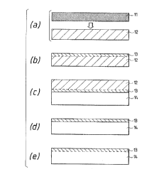
(Embodiment 1-1)
Figs. l(a) to (e) are process views for
explaining one example of the method of preparing a
semiconductor substrate of the present invention, each
shown as a schematic cross-sectional view in each
process.
According to the result of an observation by
a transmission electron microscope, micro-pores of an
average diameter of about 600A are formed in the porous
Si layer, so that the density of the layer has been
2Q~9~38
-- 19 --
l reduced half or below that of the monocrystalline Si.
Nevertheless, the monocrystallinity is still maintained,
so that it is possible to form a monocrystalline Si
layer on the porous layer by epitaxial growth. When
the temperature exceeds 1000C, rearrangement of
internal pores occurs, which impedes the acceleration
of the etching. For this reason, the epitaxial growth
of the Si layer is preferably effected by a low-
temperature growth method such as, for example, a
molecular beam epitaxial growth method, a CVD method
such as plasma CVD method, low-pressure CVD or photo
CVD method, a bias sputter method, or a liquid-phase
growth method.
A description will now be given of the method
in which after making a P-type or high-density N-type
(highly dense enough to realize the porous structure)
Si substrate entirely porous, the epitaxial growth of
a monocrystalline layer is made.
First, a P-type Si monocrystalline substrate 11
is prepared and made entirely porous, as shown in
Fig. l(a).
Next, the epitaxial growth is made on the
surface of a porous substrate 12, with one of various
growth methods, as shown in Fig. l(b), to form a thin
film monocrystalline layer 13. The P-type Si substrate
is made porous by anodization using an HF solution.
The density of the porous Si layer can be changed to
2069D38
- 20 -
l the range of 1.1 to 0.6 g/cm3 by changing the
concentration of the HF solution from 50 to 20%, as
compared with the density of 2.33 g/cm3 of
monocrystalline Si.
This porous layer is not formed on the N-type
Si layer, owing to the following reasons, but only on
the P-type Si substrate. The porous Si layer has pores
having an average size of about 600A which was measured
by observation with a transmission electron microscope.
Porous Si was discovered in the course of
research on electrolytic polishing of a semiconductor
which was conducted by Uhlir et al., in 1956 (A. Uhlir,
Bell Syst. Tech. J., vol. 35, 333 (1956)).
Unagami et al. investigated dissolving reaction
of Si during anodization and reported that the anodic
reaction of Si in an HF solution requires positive
holes, and that the reaction is expressed as follows
(T. Unagami, J. Electrochem. soc., vol. 127, 476 (1980)).
Si + 2HF + (2-n)e+ ~ SiF2 + 2H+ + ne~
SiF2 + 2HF ~ SiF4 + H2
SiF4 + 2HF ~ H2SiF6
or
Si + 4HF + (4-~)e+ ~ SiF4 + 4H+ + ~e
SiF4+ 2HF ~ H2SiF6
where e+ and e~ respectively denote a positive hole and
an electron, and n and ~ each denote the number of
positive holes required for dissolving one silicon atom.
~Q69038
- 21 -
l Porous Si can be formed when the condition, n > 2 or
> 4, is satisfied.
As above described, the P-type Si having
positive holes can be made porous, while the N-type Si
cannot be made porous. The selectivity in producing a
porous structure has been demonstrated by Nagano et al.
and Imai (Nagano, Nakajima, Yasumo, Oonaka, Kajiwara,
Electronic Communications Institute Technical Studies
Report, vol. 79, SSD79-9549 (1979)), (K. Imai, Solid-
State Electronics, vol. 24, 159 (1981)).
However, it is also reported that high-density
N-type Si can be made porous (R. P. Holmstrom and J. K.
Chi, Appl. Phys. Lett., vol. 42, 386 (1983)), so that
it is important to select a substrate which can be
made porous irrespectively of whether it is P-type
or N-type.
Porous layer is internally formed with a large
amount of gaps, resulting in the density decreasing to
half or less. Consequently, the surface area will
drastically increase as compared with that of
deposition, so that its chemical etching rate is
remarkably higher than that of the normal monocrystalline
layer.
Referring now to Fig. l(c), a light-transparent
substrate 14, which is typically a glass sheet, is
prepared as an insulating substrate, and bonded on the
surface of monocrystalline Si layer 13, to a degree of
- 22 - 2Q5~38
l pulling against each other with a Van der Waals force
(primary bonding). It will be appreciated that after
an oxide layer is formed on the surface of Si
monocrystalline layer 13, the oxide layer and the
light-transparent substrate 14 may be bonded. Also, it
will be appreciated that in place of the light-
transparent substrate 14, a substrate having an oxide
layer formed on the surface of monocrystalline Si may
be used. The bonding strength of the primary bonding
must be strong enough to retain the primary bonding
state, without yielding exfoliations in the course to
the secondary bonding to be performed later. The
primary bonding can be performed at room temperature,
or by heating, but when heating, the heating temperature
must be lower than the temperatue used for the secondary
bonding. The temperature for the secondary bonding is
suitably in a range of 200 to 800C, depending on the
material of insulating substrate.
Thereafter, the porous Si substrate 12 is
entirely etched, whereby a thinned monocrystalline Si
layer 13 is left on the light transparent substrate 14,
as shown in Fig. l(d). If the etching solution may
also etch the light-transparent glass substrate 14 in
etching, an anti-etching film must be provided on the
back surface of the light-transparent glass substrate
14, except for an instance where the light-transparent
glass substrate 14 is etched more or less, but the
- 23 - r ~ ~ 5 9 ~ 3 8
l etched surface is not different from an optically
polished surface, and an instance where the light-
transparent glass substrate 14 is not etched at all.
An Si3N4 layer is formed by deposition as the anti-
etching film to cover wholly the two adjacently placedsubstrates, and the Si3N4 layer on the porous Si
substrate is removed. It is possible to use other
materials such as Apiezon Wax~ in place of Si3N4, as
the material of the anti-etching layer.
Finally, with th~ heat treatment, Si/SiO2 layer
and light-transparent substrate 14 are bonded more
strongly for the secondary bonding. Since the thin
film and the light-transparent substrate are bonded as
above described, the thin film is bonded in alignment
with the substrate, so that it is possible to prevent
exfoliations and cracks of the substrate caused by the
difference between their thermal expansion coefficients.
Fig. l(e) shows the semiconductor substrate
obtained by this embodiment, in which a monocrystalline
Si layer 13 having a crystallinity equivalent to that
of a silicon wafer is formed on the light-transparent
substrate 14, with high degrees of smoothness and
uniformity, and with a small thickness, over a wide
area covering the whole surface of the wafer.
The semiconductor substrate thus obtained is
advantageous from the view point of production of an
insulation-isolated electronic device.
- 24 -
~2 0 ~ 9 ~ 3 ~
1 (Embodiment 1-2)
Another embodiment for the method of fabricating
a semiconductor substrate according to the prevent
invention will be described in detail with reference
to the drawings.
Figs. 2(a) to (e) are process views for
explaining another example of the method of preparing
a semiconductor substrate of the present invention,
each shown as a schematic cross-sectional view in each
process.
First, a low-carrier density layer 22 is formed
by epitaxial growth with one of various thin film
growth methods or by counter doping the surface of a
high-carrier density Si substrate 21, as shown in
Fig. 2(a). Alternatively, an N-type monocrystalline
layer 22 may be formed on the surface of a P-type Si
monocrystalline substrate 21 by ion implantation of
protons.
Then, as shown in Fig. 2(b), the P-type or
high-density N-type Si monocrystalline substrate 21 is
changed into a porous Si substrate 23 by effecting, on
the reverse side thereof, anodization using an HF
solution. The initial monocrystalline Si having the
density of 2.33 g/cm3 can be changed into a porous
member the density of which can be varied within the
range between 1.1 and 0.6 g/cm3 by varying the HF
concentra~ion of the etching solution between 50% and
206903~
- 25 -
1 20%. This porous member is formed into a P-type or
high-density N-type Si substrate, as above described.
Referring now to Fig. 2(c), a light-transparent
substrate 24, which is typically a glass sheet, is
prepared as an insulating substrate, and bonded on the
surface of Si monocrystalline layer 22, to a degree of
pulling against each other with a Van der Waals force
(primary bonding). It will be appreciated that after
an oxide layer is formed on the surface of Si
monocrystalline layer 22, the oxide layer and the
light-transparent substrate 24 may be bonded. Also,
it will be appreciated that in place of the light-
transparent substrate 24, a substrate having an oxide
layer formed on the surface of monocrystalline Si may
be used.
The bonding strength of the primary bonding
must be strong enough to retain the primary bonding
state, without yielding exfoliations in the course to
the secondary bonding to be performed later.
Thereafter, the porous Si substrate 23 is
entirely etched, whereby a thinned monocrystalline Si
layer 22 is left on the light-transparent substrate 24,
as shown in Fig. 2(d). If the etching solution may
also etch the light-transparent glass substrate 24 in
etching, an anti-etching film must be provided on the
back surface of the light-transparent glass substrate
24, except for an instance where the light-transparent
- 2 ~2 0 ~ ~ ~ 3 ~
1 glass substrate 24 is etched more or less, but the
etched surface is not different from an original
optically polished surface, and an instance where the
light-transparent glass substrate 24 is not etched at
all. An Si3N4 layer is formed by deposition as the
anti-etching film to cover the entire member composed
of the two substrates bonded together, and the Si3N4
layer on the surface of porous Si substrate is removed.
It is possible to use other materials such as Apiezon
Wax~ in place of Si3N4, as the material of the anti-
etching layer.
Finally, with the heat treatment, Si/SiO2 layer
and light-transparent substrate 14 are bonded more
strongly for the secondary bonding, as shown in
Fig. 2(e). Since the thin film and the light-
transparent substrate are bonded as above described,
the thin film is bonded in alignment with the substrate,
so that it is possible to prevent exfoliations and
cracks of the substrate caused by the difference between
their thermal expansion coefficients.
Fig. 2(e) shows the semiconductor substrate
obtained by this embodiment, in which a monocrystalline
Si layer 22 having a crystallinity equivalent to that
of a silicon wafer is formed on the light-transparent
substrate 24, with high degrees of smoothness and
uniformity, and with a small thickness, over a wide
area covering the whole surface of the wafer. The
,-, . j
2069038
- 27 -
1 semiconductor substrate thus obtained is advantageous
from the view point of production of an insulation-
isolated electronic device.
The above method is one in which an apitaxial
layer is formed before making a porous structure, and
then the regions other than the epitaxial layer are
made porous selectively by anodization.
(Embodiment 2-1)
Figs. 3(a) to (d) are process views for
explaining this embodiment, each shown as a schematic
cross-sectional view in each process.
The following will be given of a method in
which the whole P- or high-density N-type Si substrate
is changed into porous structure, and then a non-porous
monocrystal Si layer is formed on the porous structure
by epitaxial growth.
Referring to Fig. 3(a), as the first step, an
Si monocrystalline semiconductor member 31 of P-type is
prepared, and is wholly changed into porous structure 32.
Then, as shown in Fig. 3(b), an epitaxial growth
is effected by a suitable method on the surface of the
porous member 32, thereby forming a monocrystalline Si
layer 33.
Then, as shown in Fig. 3(c), the surface of the
monocrystalline Si layer 33 on the porous Si substrate
32 is oxidized to form an oxide film 35. This oxide
film 35 is formed to reduce the interface level of the
- r i O ~ ~ ~ 3 ~
1 monocrystalline layer 33 which is a final active layer.
Then, an insulating substrate 34 such as a
light-transparent glass substrate is bonded on the
surface of the oxide film 35, to a degree of pulling
against each other with a Van der Waals force, or to a
degree that bonded interfaces may not exfoliate due to
a difference between thermal expansion coefficients of
both members (primary bonding). It will be appreciated
that this insulating substrate 34 may be, in place of
the glass substrate, a substrate having an oxide layer
formed on the surface of monocrystalline Si. The
bonding strength of the primary bonding must be strong
enough to retain the primary bonding state, without
yielding exfoliations in the course to the secondary
bonding for the complete bonding to be performed later.
Thereafter, an anti-etching film 36 is provided
on the back surface of the light-transparent glass
substrate 34. An Si3N4 layer is formed by deposition
as the anti-etching film 36 to cover the entire member
composed of the two substrates bonded together, and
the Si3N4 layer on the surface of porous Si substrate
is removed. It is possible to use other materials
such as Apiezon Wax, in place of Si3N4, as the material
of the anti-etching layer.
Then, as shown in Fig. 3(d), the porous Si
substrate 32 is entirely immersed in hydrofluoric acid
with agitating so that only the porous Si is removed by
t-A `
20~9~38
- 29 -
l electroless wet chemical etching, whereby a thinned
monocrystalline silicon layer 13 is left on the light-
transparent substrate 34.
Finally, with the heat treatment, Si/SiO2 layer
and light-transparent substrate 14 are bonded more
strongly for the secondary bonding which is a complete
bonding, as shown in Fig. l(e), so that a semiconductor
member of this embodiment can be obtained by removing
the anti-etching film 36.
A description will now be given of the selective
etching method of porous Si with hydrofluoric acid used
in this embodiment.
Fig. 5 shows the etching time dependency of
etched thickness of porous Si and monocrystalline Si
when the porous Si and the monocrystalline Si are
etched by being immersed in 49% hydrofluoric acid and
agitated.
The porous Si was formed by anodizing a
monocrystalline Si. The conditions of anodization are
shown below. It is to be noted, however, that the
starting material for producing porous Si by anodization
is not limited to monocrystalline Si and Si of other
crystalline structure may be used as the starting
material.
Voltage applied : 2.6 (V)
Current density : 30 (mA-cm~2)
Anodizing solution: HF:H20:C2H50H=l:l:l
2069038
- 30 -
l Time : 2.4 hours
Thickness of porous Si: 300 (~m)
Porosity : 56 (%)
Test pieces of the porous Si thus prepared
were immersed in 49% hydrofluoric acid solution (white
circles) at the room temperature and agitated. The
reduction in the thickness of the porous Si was then
measured. The porous Si was rapidly etched: namely,
by a layer thickness of 90 ~m in 40 minutes, and
further 205 ~m in 80 minutes, with high degrees of
surface quality and uniformity.
The etching rate has dependencies on the
concentration of the etching solution and the
temperature.
Test pieces of non-porous Si having a thickness
of 500 ~m were immersed in 49% hydrofluoric acid
solution (black circles) at the room temperature and
agitated. The reduction in the thickness of the non-
porous Si was then measured. The non-porous Si was
only etched to 50A or less after elapse of 120 minutes.
The etched test pieces of porous Si and non-
porous Si were then rinsed with water and the surfaces
after the rinsing were examined by microanalysis using
secondary ions but no impurity was detected.
The conditions for the solution concentration
and the temperature were set in the range where the
etching rate of porous Si and the selection ratio of
2069038
- 31 -
l etching the porous Si and the non-porous Si have no
effect in the practical use such as a fabrication
process.
A description will be made of the etching
solution in which the porous Si is etched.
Known methods of etching porous Si are the
following two methods.
1. The method of etching porous Si with an
aqueous NaOH solution (G. Bonchil, R. Herino, K. Barla,
and J. C. Pfister, J. Electrochem. Soc., Vol. 130,
No. 7, 1611 (1983)).
2. The method of etching porous Si with an
etching solution which is capable of etching
monocrystalline Si.
In the above method 2, a fluoronitric acid-type
etching solution is generally used, and etching of Si
proceeds as follows:
Si + 20 ~ Si 2
SiO2 + 4HF ~ SiF4 + H20
That is, Si is oxidized by nitric acid to SiO2,
and the SiO2 produced is etched with hydrofluoric acid.
Examples of etching solutions for non-porous
Si include the above fluoronitric acid-type etching
solution as well as ethylenediamine-type, KOH-type and
hydrazine-type etching solutions and the like.
It will be thus understood that it is desirable
in selective etching of porous Si to select an etching
20G~03~
- 32 -
1 solution which is capable of etching porous Si, other
than the above etching solutions used for the etching
of crystalline Si. The porous Si is conventionally
selectively etched by the method which uses an aqueous
NaOH solution as an etching solution.
As above described, the porous Si is etched
with the fluoronitric acid-type etching solution, but
monocrystalline Si may be possibly etched.
In the conventional method of selectively
etching porous Si with an aqueous NaOH solution, Na
ions are inevitably adsorbed on the etched surface.
Since the Na ions cause impurity contAm;nAtion~ are
movable and have adverse effects such as the formation
of interfacial state, it is desirable that the ions
are not introduced into the semiconductor process.
In this embodiment, the etching solution is
hydrofluoric acid, which has no etching action on the
non-porous Si, but is used in an ordinary semiconductor
process, with quite less etching contamination.
Thus, in this embodiment, it is possible to
selectively etch the porous Si, but not the non-porous
Si, by the chemical etching with high degrees of
efficiency and uniformity, without having no adverse
effects on the process.
(Embodiment 2-2)
Figs. 4(a) to (e) are process views for
explaining this embodiment, each shown as a schematic
2069038
- 33 -
l cross-sectional view in each process.
First, a low-carrier density layer 42 is formed
by epitaxial growth with one of various thin film
growth methods or by counter doping the surface of a
high-carrier density Si substrate 41, as shown in
Fig. 4(a). Alternatively, an N-type monocrystalline
layer 42 may be formed on the surface of a P-type Si
monocrystalline substrate 41 by ion implantation of
protons.
Then, as shown in Fig. 4(b), the P-type or
high-density N-type Si monocrystalline substrate 41 is
changed into a porous Si substrate 43 by effecting, on
the reverse side thereof, anodization using an HF
solution. The initial monocrystalline Si having the
lS density of 2.33 g/cm3 can be changed into a porous
member the density of which can be varied within the
range between 1.1 and 0.6 g/cm3 by varying the HF
concentration of the etching solution between 50% and
20%. This porous member is formed into a P-type or
high-density N-type Si substrate, as above described.
Referring now to Fig. 4(c), a light-transparent
substrate 44, which is typically a glass sheet, is
prepared as an insulating substrate, and after oxidizing
the surface of monocrystalline Si layer on a porous Si
substrate, bonded on the oxidized surface at the room
temperature or by heating, to a degree of pulling
against each other with a Van der Waals force or to a
- 34 -
F 2 ~ 6 ~
l degree that the bonded interfaces may not exfoliate due
to a difference between thermal expansion coefficients
of both members (primary bonding). It will be
appreciated that in place of the light-transparent
substrate 34, a substrate having an oxide layer formed
on the surface of monocrystalline Si may be used. The
bonding strength of the primary bonding must be strong
enough to retain the primary bonding state, without
yielding exfoliations in the course to the secondary
bonding for the complete bonding to be performed later.
The oxide layer 45 on the surface of monocrystalline
layer is formed to reduce the interface level of the
monocrystalline layer 42 which is a final active layer.
Thereafter, an anti-etching film 46 is provided
on the back surface of the light-transparent glass
substrate 44. An Si3N4 layer is formed by deposition
as the anti-etching film to cover the entire member
composed of the two substrates bonded together, and
the Si3N4 layer on the surface of porous Si substrate
is removed. It is possible to use other materials
such as ApiezonWax~, in place of Si3N4, as the material
of the anti-etching layer.
Then, as shown in Fig. 4(d), the porous Si
substrate 43 is entirely immersed in hydrofluoric acid,
with agitating so that only the porous Si is etched by
electroless wet chemical etching, whereby a thinned
monocrystalline Si layer 42 is left on the light-
.
_ 35 20S~0~
1 transparent substrate 44.
Finally, with the heat treatment, Si/SiO2 layer
and light-transparent substrate 44 are bonded completely
in the secondary bonding.
s Since the thin film and the light-transparent
substrate are bonded as above described, the thin film
is bonded in alignment with the substrate, so that it
is possible to prevent exfoliations and cracks of the
substrate caused by the difference between their
thermal expansion coefficients.
Fig. 4(e) shows the semiconductor substrate
obtained by this embodiment, in which a monocrystalline
Si layer 42 having a crystallinity equivalent to that
of a silicon wafer is formed on the light-transparent
substrate 44, with high degrees of smoothness and
uniformity, and with a small thickness, over a wide
area covering the whole surface of the wafer. The
semiconductor substrate thus obtained is advantageous
from the view point of production of an insulation-
isolated electronic device.
The conditions for the solution concentrationand the temperature were set in the range where the
etching rate of porous Si and the selection ratio of
etching the porous Si and the non-porous Si have no
effect in the practical use such as a fabrication
process.
The above method is one in which an epitaxial
20~9~38
- 36 -
l layer is formed before making a porous structure, and
then the regions other than the epitaxial layer are
made porous selectively by anodization.
The above embodiments 2-1 and 2-2 are provided
with the oxide layers 35, 45 and the anti-etching films
36, 46, but can be realized without them, with the same
effects of the present invention.
The etching rate has dependencies on the
concentration of the etching solution and the
temperature. The etching solution concentration and
temperature are suitably determined in practical ranges.
In the embodiments 2-1 and 2-2, 49% hydrofluoric acid
and the room temperature are used, but the present
invention is not limited to such conditions.
Preferably, the concentration of the hydrofluoric acid
is 5% to 95%, and the temperature is set to a level
which is ordinarily adopted.
(Embodiment 3-1)
The etching can be made using a mixture liquid
of hydrofluoric acid and alcohol, in place of
hydrofluoric acid used for an etching solution in
embodiments 2-1 and 2-2. In this case, porous Si can
be selectively etched with high degrees of efficiency
and uniformity, without etching non-porous Si, as in
the embodiments 2-1 and 2-2.
Fig. 6 shows the time dependency of etching
thickness of porous Si and monocrystalline Si as
- 2069~38
- 37 -
1 observed when the porous Si and the monocrystalline Si
are etched by being immersed in the mixture liquid
(10:1) of 49% hydrofluoric acid and alcohol without
agitation of the liquid.
The porous Si was formed by anodizing the
monocrystalline Si. The conditions of anodization are
shown below. It is to be noted, however, that the
starting material for producing porous Si by anodization
is not limited to monocrystalline Si and Si of other
crystalline structure may be used as the starting
material.
Voltage applied : 2.6 (V)
Current density : 30 (mA-cm 2)
Anodizing solution : HF:H2O:C2H5OH=l:l:l
Time : 2.4 hours
Thickness of porous Si: 300 (~m)
Porosity : 56 (%)
Test pieces of the porous Si prepared as
described above were immersed, without agitation, in a
mixture solution (10:1) of 49% hydrofluoric acid and
alcohol (white circles). The reduction in the
thickness of the porous Si was then measured. The
porous Si was rapidly etched: namely, by a layer
thickness of 85 ~m in 40 minutes, and further 195 ~m
in 80 minutes, with high degrees of surface quality and
uniformity. The etching rate has dependencies on the
concentration of the etching solution and the temperature.
2069~338
- 38 -
1 Test pieces of non-porous Si having a thickness
of 500 ~m were immersed in a mixture liquid (10:1) of
49% hydrofluoric acid and alcohol (black circles) at
the room temperature without agitation. The reduction
in the thickness of the non-porous Si was then measured.
The non-porous Si was only etched to 50A or less after
elapse of 120 minutes.
In particular, the addition of alcohol serves
to remove bubbles of reaction product gases generated
as a result of the etching without delay from the
surface being etched, without necessitating agitation,
thus ensuring a high efficiency and uniformity of the
etching.
The etched test pieces of porous Si and non-
porous Si were then rinsed with water and the surfacesafter the rinsing were examined by microanalysis using
secondary ions but no impurity was detected.
The conditions for the concentration of etching
solution and the temperature were set in the range
where the etching rate has no effect in the practical
use such as a fabrication process, and alcohol can
exhibit its effects. Although the mixture solution
(10:1) of 49% hydrofluoric acid and ethyl alcohol, as
well as the room temperature as the solution temperature,
are mentioned, the present invention is not limited to
such conditions.
The HF concentration with respect to the etching
2069038
- 39 -
1 solution preferably ranges between 1 and 95%, more
preferably between 5 and 90%, and most preferably
between 5 and 80%. The alcohol concentration with
respect to the etching solution is preferably 80% or
less, more preferably 60% or less, and most preferably
40% or less, and is determined so as to provide an
appreciable effect of alcohol. The temperature is set
in a range of preferably 0 to 100C, more preferably 5
to 80C, and most preferably 5 to 60C.
Although ethyl alcohol has been used in this
invention, other alcohols such as isopropyl alcohol,
which does not cause any inconvenience in the commercial
production and which can provide an appreciable effect
of addition of such alcohol, may be used as the alcohol.
(Embodiment 3-2)
The etching can be made using a mixture liquid
of hydrofluoric acid and hydrogen peroxide, in place of
hydrofluoric acid used for an etching solution in
embodiments 2-1 and 2-2. In this case, porous Si can
be selectively etched with high degrees of efficiency
and uniformity, without etching non-porous Si, as in
the embodiments 2-1 and 2-2.
The selective etching of porous Si will be
described below with a mixture solution of hydrofluoric
acid and hydrogen peroxide for use in this embodiment.
Fig. 7 shows the time dependency of etching
thickness of porous Si and monocrystalline Si as
2069038
- 40 -
l observed when the porous Si and the monocrystalline Si
are etched by being immersed in a mixture liquid (1:5)
of 49% hydrofluoric acid and 30% hydrogen peroxide and
agitated.
The porous Si was formed by anodizing the
monocrystalline Si. The conditions of anodization are
shown below. It is to be noted, however, that the
starting material for producing porous Si by anodization
is not limited to monocrystalline Si and Si of other
crystalline structure may be used as the starting
material.
Voltage applied : 2.6 (V)
Current density : 30 (mA cm 2)
Anodizing solution : HF:H2O:C2H5OH=l:l:l
Time : 2.4 hours
Thickness of porous Si: 300 (~m)
Porosity : 56 (%)
Test pieces of the porous Si prepared as
described above were immersed, without agitation, in
the mixture solution (1:5) of 49% hydrofluoric acid
and 30% hydrogen peroxide (white circles) at the room
temperature. The reduction in the thickness of the
porous Si was then measured. The porous Si was rapidly
etched: namely, by a layer thickness of 112 ~m in 40
minutes, and further 256 ~m in 80 minutes, with high
degrees of surface quality and uniformity. The etching
rate has dependencies on the concentration of the
2069038
- 41 -
l etching solution and the temperature.
Test pieces of non-porous Si having a thickness
of 500 ~m were immersed in the mixture liquid (1:5) of
49% hydrofluoric acid and 30% hydrogen peroxide (black
circles) at the room temperature and agitated. The
reduction in the thickness of the non-porous Si was
then measured. The non-porous Si was only etched to
50A or less after elapse of 120 minutes.
In particular, the addition of hydrogen peroxide
serves to accelerate oxidation of silicon, thus
enhancing the reaction speed as compared to the case
where hydrogen peroxide is not added. Furthermore,
the reaction speed can be controlled by suitably
selecting the content of the hydrogen peroxide.
The etched test pieces of porous Si and non-
porous Si were then rinsed with water and the surfaces
after the rinsing were examined by microanalysis using
secondary ions but no impurity was detected.
Although the concentration of hydrogen peroxide
solution was 30% herein, it can be set to fall within
the ranges which would not impair the addition effect
of hydrogen peroxide and cause any practical
inconvenience in commercial production.
The etching rate has dependencies on the
solution concentrations of hydrofluoric acid and
hydrogen peroxide, as well as the temperature. The
addition of hydrogen peroxide solution makes it
2069~38
- 42 -
l possible to accelerate the oxidation of silicon, and
the reaction speed as compared to the case when it is
not added. Further, the reaction speed can be
controlled by suitably selecting the content of the
hydrogen peroxide.
The conditions for the concentration of etching
solution and the temperature can be set to fall within
the ranges in which the effects of hydrofluoric acid
and hydrogen peroxide solution can be exhibited and
the etching rate would not cause any practical
inconvenience in commercial production. Although the
mixture solution (1:5) of 49% hydrofluoric acid and
hydrogen peroxide, as well as the room temperature as
the solution temperature, are mentioned as an instance,
the present invention is not limited to such conditions.
The HF concentration with respect to the etching
solution preferably ranges between 1 and 95%, more
preferably between 5 and 90%, and most preferably
between 5 and 80%. The H2O2 concentration with respect
to the etching solution preferably ranges between 1 and
95%, more preferably between 5 and 90%, and most
preferably between 10 and 80%, and is determined so as
to provide an appreciable effect of hydrogen peroxide.
The temperature is set in a range of preferably 0 to
100C, more preferably 5 to 80C, and most preferably
5 to 60C.
2~69n38
- 43 -
1 (Embodiment 3-3)
The etching can be made using a mixture liquid
of hydrofluoric acid, alcohol and hydrogen peroxide, in
place of hydrofluoric acid used for an etching solution
in embodiments 2-1 and 2-2. In this case, porous Si
can be selectively etched with high degrees of efficiency
and uniformity, without etching non-porous Si, as in the
embodiments 2-1 and 2-2.
The selective etching of porous Si will be
described below with a mixture solution of hydrofluoric
acid, alcohol and hydrogen peroxide for use in this
embodiment.
Fig. 8 shows the time dependency of etching
thickness of porous Si and monocrystalline Si as
observed when the porous Si and the monocrystalline Si
are etched by being immersed in a mixture liquid
(10:6:50) of 49% hydrofluoric acid, alcohol and 30%
hydrogen peroxide without agitation.
The porous Si was formed by anodizing the
monocrystalline Si. The conditions of anodization are
shown below. It is to be noted, however, that the
starting material for producing porous Si by anodization
is not limited to monocrystalline Si and Si of other
crystalline structure may be used as the starting
material.
Voltage applied: 2.6 (V)
Current density: 30 (mA-cm 2)
2069038
l Anodizing solution : HF:H2O:C2H5OH=1:1:1
Time : 2.4 hours
Thickness of porous Si: 300 (~m)
Porosity : 56 (%)
Test pieces of the porous Si prepared as
described above were immersed, without agitation, in
the mixture solution (10:6:5) of 49% hydrofluoric acid,
alcohol and 30% hydrogen peroxide (white circles) at
the room temperature. The reduction in the thickness
of the porous Si was then measured. The porous Si was
rapidly etched: namely, by a layer thickness of 107 ~m
in 40 minutes, and further 244 ~m in 80 minutes, with
high degrees of surface quality and uniformity. The
etching rate has dependencies on the concentration of
the etching solution and the temperature.
Test pieces of non-porous Si having a thickness
of 500 ~m were immersed in the mixture liquid (10:6:5)
of 49% hydrofluoric acid, alcohol and 30% hydrogen
peroxide (black circles) at the room temperature
without agitation. The reduction in the thickness of
the non-porous Si was then measured. The non-porous
Si was only etched to 50A or less after elapse of 120
minutes.
The etched test pieces of porous Si and non-
porous Si were then rinsed with water and the surfaces
after the rinsing were examined by microanalysis using
secondary ions but no impurity was detected.
20~9038
- 45 -
l Although the concentration of hydrogen peroxide
solution was 30% herein, it can be set to fall within
the ranges which would not impair the addition effect
of hydrogen peroxide and cause any practical
inconvenience in commercial production.
The etching rate has dependencies on the solution
concentrations of hydrofluoric acid and hydrogen
peroxide, as well as the temperature. The addition of
hydrogen peroxide solution makes it possible to
accelerate the oxidation of silicon, and the reaction
speed as compared to the case when it is not added.
Further, the reaction speed can be controlled by
suitably selecting the content of the hydrogen peroxide.
In particular, the addition of alcohol serves to remove
bubbles of reaction product gases generated as a result
of the etching without delay from the surface being
etched, without necessitating agitation, thus ensuring
a high efficiency and uniformity of the etching for the
porous Si.
The conditions for the concentration of etching
solution and the temperature can be set to fall within
the ranges in which the effects of hydrofluoric acid,
hydrogen peroxide solution and alcohol can be exhibited
and the etching rate would not cause any practical
inconvenience in commercial production. Although the
mixture solution (10:6:5) of 49% hydrofluoric acid,
ethyl alcohol and hydrogen peroxide, as well as the
- 46 - 20~03~
l room temperature as the solution temperature, are
mentioned as an instance, the present invention is
not limited to such conditions.
The HF concentration with respect to the etching
solution preferably ranges between 1 and 95%, more
preferably between 5 and 90%, and most preferably
between 5 and 80%. The H2O2 concentration with respect
to the etching solution preferably ranges between 1 and
95%, more preferably between 5 and 90%, and most
preferably between 10 and 80%, and is determined so as
to provide an appreciable effect of hydrogen peroxide.
The alcohol concentration with respect to the etching
solution is preferably 80% or less, more preferably 60%
or less, and most preferably 40% or less, and is
determined so as to provide an appreciable effect of
alcohol. The temperature is set in a range of
preferably 0 to 100C, more preferably 5 to 80C, and
most preferably 5 to 60C.
Although ethyl alcohol has been specifically
used in this invention, other alcohols such as isopropyl
alcohol, which does not cause any inconvenience in the
commercial production and which can provide an
appreciable effect of addition of such alcohol, may
be used as the alcohol.
(Embodiment 3-4)
The etching can be made using a buffered
hydrofluoric acid, in place of hydrofluoric acid used
2069()38
- 47 -
l for an etching solution in embodiments 2-1 and 2-2. In
this case, porous Si can be selectively etched with
high degrees of efficiency and uniformity, without
etching non-porous Si, as in the embodiments 2-1 and
2-2.
The selective etching of porous Si will be
described below with the buffered hydrofluoric acid for
use in this embodiment.
Fig. 9 shows the time dependency of etching
thickness of porous Si and monocrystalline Si as
observed when the porous Si and the monocrystalline Si
are etched by being immersed in buffered hydrofluoric
acid (a mixture solution of 4.5% hydrofluoric acid and
36% ammonium fluoride) and agitated.
The porous Si was formed by anodizing the
monocrystalline Si. The conditions of anodization are
shown below. It is to be noted, however, that the
starting material for producing porous Si by anodization
is not limited to monocrystalline Si and Si of other
crystalline structure may be used as the starting
material.
Voltage applied : 2.6 (V)
Current density : 30 (mA-cm 2)
Anodizing solution HF H2O C2H5OH 1:1:1
~~ 25 Time : 2.4 hours
Thickness of porous Si: 300 (~m)
Porosity : 56 (%)
2~69~38
- 48 -
l Test pieces of the porous Si prepared as
described above were immersed, without agitation, in
the buffered hydrofluoric acid (a mixture solution of
4.5% hydrofluoric acid and 36% ammonium fluoride) (white
circles) at the room temperature. The reduction in the
thickness of the porous Si was then measured. The
porous Si was rapidly etched: namely, by a layer
thickness of 70 ~m in 40 minutes, and further 118 ~m in
120 minutes, with high degrees of surface quality and
uniformity. The etching rate has dependencies on the
concentration of the etching solution and the
temperature.
Test pieces of non-porous Si having a thickness
of 500 ~m were immersed in the buffered hydrofluoric
acid (a mixture solution of 4.5% hydrofluoric acid and
36% ammonium fluoride) (black circles) at the room
temperature and agitated. The reduction in the
thickness of the non-porous Si was then measured. The
non-porous Si was only etched to 50A or less after
elapse of 120 minutes.
The etched test pieces of porous Si and non-
porous Si were then rinsed with water and the surfaces
after the rinsing were examined by microanalysis using
secondary ions but no impurity was detected.
~-~ 25 The buffered hydrofluoric acid is a mixture
solution of 36% ammonium fluoride (NH4F) and 4.5%
hydrogen fluoride.
2069038
- 49 -
1 The etching rate has dependencies on the
solution concentrations, as well as the temperature.
The conditions for the concentration of etching solution
and the temperaure can be set to fall within the ranges
in which no practical inconvenience would not be caused
in commercial production. Although the buffered
hydrofluoric acid cont~;n;ng a solution of 36% ammonium
fluoride (NH4F) and 4.5% hydrogen fluoride (HF), as
well as the room temperature as the solution temperature,
are mentioned as an instance, the present invention is
not limited to such conditions.
The HF concentration in the buffered
hydrofluoric acid with respect to the etching solution
preferably ranges between 1 and 95%, more preferably
between 1 and 85%, and most preferably between 1 and
70%. The NH4F concentration in the buffered
hydrofluoric acid with respect to the etching solution
preferably ranges between 1 and 95%, more preferably
between 5 and 90%, and most preferably between 5 and
80%. The temperature is set in a range of preferably
0 to 100C, more preferably 5 to 80C, and most
preferably 5 to 60C.
(Embodiment 3-5)
The etching can be made using a mixture solution
~ 25 of buffered hydrofluoric acid and alcohol, in place of
hydrofluoric acid used for an etching solution in
embodiments 2-1 and 2-2. In this case, porous Si can
20~9338
- 50 -
1 be selectively etched with high degrees of efficiency
and uniformity, without etching non-porous Si, as in
the embodiments 2-1 and 2-2.
The selective etching of porous Si will be
described below with the mixture solution of buffered
hydrofluoric acid and alcohol for use in this embodiment.
Fig. 10 shows the time dependency of etching
thickness of porous Si and monocrystalline Si as
observed when the porous Si and the monocrystalline Si
are etched by being immersed in the mixture solution
(10:1) of buffered hydrofluoric acid (a mixture
solution of 4.5% hydrofluoric acid and 36% ammonium
fluoride) and alcohol without agitation.
The porous Si was formed by anodizing the
monocrystalline Si. The conditions of anodization are
shown below. It is to be noted, however, that the
starting material for producing porous Si by anodization
is not limited to monocrystalline Si and Si of other
crystalline structure may be used as the starting
20 material.
Voltage applied : 2.6 (V)
Current density : 30 (mA cm~2)
Anodizing solution HF H20 C2H5H 1:1:1
Time : 2.4 hours
~ ~ 25 Thickness of porous Si: 300 (~m)
Porosity : 56 (%)
Test pieces of the porous Si prepared as
2069~38
1 described above were immersed, without agitation, in
the mixture solution (10:1) of buffered hydrofluoric
acid (a mixture solution of 4.5% hydrofluoric acid and
36~ ammonium fluoride) and alcohol (white circles) at
the room temperature. The reduction in the thickness
of the porous Si was then measured. The porous Si was
rapidly etched: namely, by a layer thickness of 83 ~m
in 40 minutes, and further 140 ~m in 120 minutes, with
high degrees of surface quality and uniformity. The
etching rate has dependencies on the concentration of
the etching solution and the temperature.
Test pieces of non-porous Si having a thickness
of 500 ~m were immersed in the mixture solution of
buffered hydrofluoric acid (a mixture solution of 4.5~
hydrofluoric acid and 36% ammonium fluoride) and alcohol
(black circles) at the room temperature without
agitation. The reduction in the thickness of the non-
porous Si was then measured. The non-porous Si was
only etched to 50A or less after elapse of 120 minutes.
The etched test pieces of porous Si and non-
porous Si were then rinsed with water and the surfaces
after the rinsing were examined by microanalysis using
secondary ions but no impurity was detected.
The etching rate has dependencies on the
~ 25 solution concentrations of buffered hydrofluoric acid,
as well as the temperature. The addition of alcohol
serves to remove bubbles of reaction product gases
2069~38
1 generated as a result of the etching without delay from
the surface being etched, without necessitating
agitation, thus ensuring a high efficiency and
uniformity of the etching for the porous Si.
The conditions for the concentration of etching
solution and the temperature can be set to fall within
the ranges in which the etching rate would cause no
practical inconvenience in commercial production, with
an appreciable effect of alcohol. Although the mixture
solution (10:1) of buffered hydrofluoric acid (a mixture
solution of 4.5% hydrogen fluoride and 36% ammonium
fluoride) and ethyl alcohol, as well as the room
temperature as the solution temperature, are mentioned
as an instance, the present invention is not limited to
such conditions.
The HF concentration in the buffered hydrofluoric
acid with respect to the etching solution preferably
ranges between 1 and 95%, more preferably between 1 and
85%, and most preferably between 1 and 70%. The ammonium
fluoride (NH4F) concentration in the buffered
hydrofluoric acid with respect to the etching solution
preferably ranges between 1 and 95%, more preferably
between 5 and 90%, and most preferably between 5 and
80%.
The alcohol concentration with respect to the
etching solution is preferably 80% or less, more
preferably 60% or less, and most preferably 40% or less,
2069038
- 53 -
l and is determined so as to provide an appreciable effect
of alcohol.
The temperature is set in a range of preferably
0 to 100C, more preferably 5 to 80C, and most
preferably 5 to 60C.
Although ethyl alcohol has been specifically
used in this invention, other alcohols such as isopropyl
alcohol, which does not cause any inconvenience in the
commercial production and which can provide an
appreciable effect of addition of such alcohol, may be
used as the alcohol.
(Embodiment 3-6)
The etching can be made using a mixture solution
of buffered hydrofluoric acid and hydrogen peroxide, in
place of hydrofluoric acid used for an etching solution
in embodiments 2-1 and 2-2. In this case, porous Si
can be selectively etched with high degrees of
efficiency and uniformity, without etching non-porous
Si, as in the embodiments 2-1 and 2-2.
The selective etching of porous Si will be
described below with the mixture solution of buffered
hydrofluoric acid and hydrogen peroxide for use in this
embodiment.
Fig. 11 shows the time dependency of etching
thickness of porous Si and monocrystalline Si as
observed when the porous Si and the monocrystalline Si
are etched by being immersed in the mixture solution
~06~038
- 54 -
l (1:5) of buffered hydrofluoric acid (a mixture solution
of 4.5% hydrofluoric acid and 36% ammonium fluoride)
and 30% hydrogen peroxide and agitated.
The porous Si was formed by anodizing the
monocrystalline Si. The conditions of anodization are
shown below. It is to be noted, however, that the
starting material for producing porous Si by anodization
is not limited to monocrystalline Si and Si of other
crystalline structure may be used as the starting
10 material.
Voltage applied : 2.6 (V)
Current density : 30 (mA-cm 2)
Anodizing solution : HF:H2O:C2H5OH=1:1:1
Time : 2.4 hours
Thickness of porous Si: 300 (~m)
Porosity : 56 (~) -
Test pieces of the porous Si prepared as
described above were immersed, with agitation, in the
mixture solution (1:5) of buffered hydrofluoric acid
(a mixture solution of 4.5% hydrofluoric acid and 36%
ammonium fluoride) and 30~ hydrogen peroxide (white
circles) at the room temperature. The reduction in
the thickness of the porous Si was then measured. The
porous Si was rapidly etched: namely, by a layer
--~ 25 thickness of 88 ~m in 40 minutes, and further 147 ~m
in 120 minutes, with high degrees of surface quality
and uniformity. The etching rate has dependencies on
2069038
- 55 -
l the concentration of the etching solution and the
temperature.
Test pieces of non-porous Si having a thickness
of 500 ~m were immersed in the mixture solution (1:5) of
buffered hydrofluoric acid (a mixture solution of 4.5%
hydrofluoric acid and 36% ammonium fluoride) and 30%
hydrogen peroxide (black circles) at the room
temperature and agitated. The reduction in the
thickness of the non-porous Si was then measured. The
non-porous Si was only etched to 50A or less after
elapse of 120 minutes.
The etched test pieces of porous Si and non-
porous Si were then rinsed with water and the surfaces
after the rinsing were exAmined by microanalysis using
secondary ions but no impurity was detected.
Although the solution concentration of hydrogen
peroxide was 30% herein, it can be set to fall within
the ranges in which it would provide an appreciable
effect of the addition of hydrogen peroxide and have
no practical inconvenience in commercial production.
The etching rate has dependencies on the
solution concentrations of buffered hydrofluoric acid
and hydrogen peroxide, as well as the temperature. The
addition of hydrogen peroxide solution makes it possible
~ 25 to accelerate the oxidation of silicon, and the reaction
speed as compared to the case when it is not added.
Further, the reaction speed can be controlled by
206S038
- 56 -
l suitably selecting the content of the hydrogen peroxide.
The conditions for the concentration of etching
solution and the temperature can be set to fall within
the ranges in which they provide an appreciable effect
of buffered hydrofluoric acid and hydrogen peroxide and
the etching rate would cause no practical inconvenience -
in commercial production. Although the mixture solution
(1:5) of buffered hydrofluoric acid and hydrogen
peroxide, as well as the room temperature as the
solution temperature, are mentioned as an instance, the
present invention is not limited to such conditions.
The HF concentration in the buffered hydrofluoric
acid with respect to the etching solution preferably
ranges between 1 and 95%, more preferably between 1 and
85%, and most preferably between 1 and 70%.
The H2O2 concentration with respect to the
etching solution preferably ranges between 1 and 95%,
more preferably between 5 and 90%, and most preferably
between 5 and 80%, and is determined so as to provide
an appreciable effect of hydrogen peroxide.
The temperature is set in a range of preferably
0 to 100C, more preferably 5 to 80C, and most
preferably 5 to 60C.
(Embodiment 3-7)
The etching can be made using a mixture solution
of buffered hydrofluoric acid, alcohol and hydrogen
peroxide, in place of hydrofluoric acid used for an
2069038
- 57 -
l etching solution in embodiments 2-1 and 2-2. In this
case, porous Si can be selectively etched with high
degrees of efficiency and uniformity, without etching
non-porous Si, as in the embodiments 2-1 and 2-2.
The selective etching of porous Si will be
described below with the mixture solution of buffered
hydrofluoric acid, alcohol and hydrogen peroxide for
use in this embodiment.
Fig. 12 shows the time dependency of etching
thickness of porous Si and monocrystalline Si as
observed when the porous Si and the monocrystalline Si
are etched by being immersed in the mixture solution
(10:6:50) of buffered hydrofluoric acid (a mixture
solution of 4.5% hydrofluoric acid and 36~ ammonium
fluoride), alcohol and 30~ hydrogen peroxide without
agitation.
The porous Si was formed by anodizing the
monocrystalline Si. The conditions of anodization are
shown below. It is to be noted, however, that the
starting material for producing porous Si by
anodization is not limited to monocrystalline Si and
Si of other crystalline structure may be used as the
starting material.
Voltage applied : 2.6 (V)
-- 25 Current density : 30 (mA-cm 2)
Anodizing solution: HF:H2O:C2H5OH=1:1:1
Time : 2.4 hours
2069~38
- 58 -
l Thickness of porous Si: 300 (~m)
Porosity : 56 (%)
Test pieces of the porous Si prepared as
described above were immersed, without agitation, in
the mixture solution (10:6:50) of buffered hydrofluoric
acid (a mixture solution of 4.5% hydrofluoric acid and
36~ ammonium fluoride), alcohol and 30% hydrogen
peroxide (white circles) at the-room temperature. The
reduction in the thickness of the porous Si was then
measured. The porous Si was rapidly etched: namely, by
a layer thickness of 83 ~m in 40 minutes, and further
140 ~m in 120 minutes, with high degrees of surface
quality and uniformity. The etching rate has
dependencies on the concentration of the etching
solution and the temperature.
Test pieces of non-porous Si having a thickness
of 500 ~m were immersed in the mixture solution (10:6:50)
of buffered hydrofluoric acid (a mixture solution of
4.5% hydrofluoric acid and 36~ ammonium fluoride),
Z0 alcohol and 30~ hydrogen peroxide (black circles) at
the room temperature without agitation. The reduction
in the thickness of the non-porous Si was then measured.
The non-porous Si was only etched to 50A or less after
elapse of 120 minutes.
~- 25 The etched test pieces of porous Si and non-
porous Si were then rinsed with water and the surfaces
after the rinsing were examined by microanalysis using
2069038
- 59 -
1 secondary ions but no impurity was detected.
Although the solution concentration of hydrogen
peroxide was 30~ herein, it can be set to fall within
the ranges in which it would provide an appreciable
effect of the addition of hydrogen peroxide and have
no practical inconvenience in commercial production.
The etching rate has dependencies on the
solution concentrations of hydrofluoric acid and
hydrogen peroxide, as well as the temperature. The
addition of hydrogen peroxide solution makes it possible
to accelerate the oxidation of silicon, and the reaction
speed as compared to the case when it is not added.
Further, the reaction speed can be controlled by suitably
selecting the content of the hydrogen peroxide.
The addition of alcohol serves to remove bubbles
of reaciton product gases generated as a result of the
etching without delay from the surface being etched,
without necessitating agitation, thus ensuring a high
efficiency and uniformity of the etching for the porous
Si.
The conditions for the concentration of etching
solution and the temperature can be set to fall within
the ranges in which they provide an appreciable effect
of buffered hydrofluoric acid, hydrogen peroxide and
alcohol, and the etching rate would cause no practical
inconvenience in commercial production. Although the
mixture solution (10:6:50) of buffered hydrofluoric
2069038
- 60 -
l acid, ethyl alcohol and hydrogen peroxide, as well as
the room temperature as the solution temperature, are
mentioned as an instance, the present invention is not
limited to such conditions.
The HF concentration in the buffered hydrofluoric
acid with respect to the etching solution preferably
ranges between 1 and 95%, more preferably between 5 and
90%, and most preferably between 5 and 80%. The H2O2
concentration with respect to the etching solution
preferably ranges between 1 and 95%, more preferably
between 5 and 90%, and most preferably between 10 and
80%, and is determined so as to provide an appreciable
effect of hydrogen peroxide.
The alcohol concentration with respect to the
etching solution is preferably 80% or less, more
preferably 60% or less, and most preferably 40% or less,
and is determined so as to provide an appreciable
effect of alcohol.
The temperature is set in a range of preferably
0 to 100C, more preferably 5 to 80C, and most
preferably 5 to 60C.
Although ethyl alcohol has been specifically
used in this invention, other alcohols such as
isopropyl alcohol, which does not cause any
~~ 25 inconvenience in the commercial production and which
can provide an appreciable effect of addition of such
alcohol, may be used as the alcohol.
2069038
- 61 -
l The specific examples of the present invention
will be described below in detail, but the present
invention is not limited to those examples.
(Example 1) (example not forming an oxide layer)
This example will be explained in accordance
with a process of Fig. 1.
First, anodization was conducted on a P-type or
N-type (100) monocrystalline Si substrate having a
thickness of 200 ~m and a specific resistance of
0.01 Q-cm in a 50% HF solution. At this time, the
current density was 100 mA/cm2. Also, the porous
structure formation rate was 8.4 ~m/min, and hence it
took twenty four minutes for the (100) Si substrate
having a thickness of 200 ~m to be made entirely porous
(Fig. l(a)).
A 0.5 ~m thick Si epitaxial layer 13 of 0.063
Q-cm was grown at a low temperature on the (100) porous
Si substrate with MBE (Molecular Beam Epitaxy) method.
Deposition was conducted under the following conditions
(Fig. l(b)).
Temperature: 700C
Pressure : lxlO 9 Torr
Growth rate: 0.1 nm/sec
Next, an optically polished fused silica glass
~ 25 substrate 14 was placed on the surface of this epitaxial
layer, and contacted thereto (Fig. l(c)).
The etching speed of the Si monocrystal having
2069038
- 62 -
l a specific resistance of 0.01 Q cm with a hydrofluoro-
nitro-acetic acid solution (49~ hydrofluoric acid: 7~%
nitric acid: 99.5% acetic acid = 1:3:8) is about 1 ~m
or less per minute, but the Si monocrystal 13 of
0.063 Q-cm can be hardly etched in this etching solution.
The etching speed of the porous layer is increased to
about 100 times thereof, as previously described. That
is, the porous Si substrate having a thickness of
200 ~m was removed in 2 minutes with a result that the
monocrystalline Si layer 13 having a thickness of 0.5 ~m
remained on the fused silica glass substrate 14. There
was no change on the epitaxial layer 13. The back
surface of the fused silica glass substrate 14 was
etched 0.1 ~m, but its front surface did not have any
difference from its original optical polished face
(Fig. l(d)).
Then, the SOI thin film layer 13 and the fused
silica glass substrate 14 were firmly joined by heating
them at 800C for 0.5 hour in an oxygen atmosphere
(Fig. l(e)).
Observing the cross-section with a transmission
electron microscope, it was confirmed that no crystal
defects were newly introduced into the Si layer and
excellent crystallinity was maintained.
~~ 25 (Example 2)
First, anodization was conducted on a P-type or
N-type (100) monocrystalline Si substrate having a
2069038
- 63 -
l thickness of 200 ~m and a specific resistance of
0.01 Q cm in a 50% HF solution. At this time, the
current density was 100 mA/cm2. Also, the porous
structure formation rate was 8.4 ~m/min and hence it
took twenty four minutes for the (lO0) Si substrate
having a thickness of 200 ~m to be made entirely porous
(Fig. l(a)).
A 0.5 ~m thick Si epitaxial layer 13 of
0.063 Q-cm was grown at a low temperature on the (100)
porous Si substrate with MBE (Molecular Beam Epitaxy)
method. Deposition was conducted under the following
conditions (Fig. l(b)).
Temperature: 700C
Pressure : lxlO 9 Torr
Growth rate: 0.1 nm/sec
Next, the surface of this epitaxial layer was
oxidized, and then an optically polished fused silica
glass substrate 14 was placed on the surface of the
oxidized film, and contacted thereto (Fig. l(c)).
The etching speed of the Si monocrystal having
a specific resistance of 0.01 Q-cm with a hydrofluoro-
nitro-acetic acid solution (49% hydrofluoric acid: 70%
nitric acid: 99.5% acetic acid = 1:3:8) is about 1 ~m
or less per minute, but the Si monocrystal 13 of
~ 25 0.063 Q-cm can be hardly etched in this etching
solution. The etching speed of the porous layer is
increased to about 100 times thereof, as previously
2069~38
- 64 -
l described. That is, the porous Si substrate having a
thickness of 200 ~m was removed in 2 minutes with a
result that the monocrystalline Si layer 13 having a
thickness of 0.5 ~m remained on the fused silica glass
substrate 14. There was no change on the epitaxial
layer 13. The back surface of the fused silica glass
substrate 14 was etched 0.1 ~m, but its front surface
did not have any difference from its original optical
polished face (Fig. l(d)).
Then, the SOI thin film layer 13 and the fused
silica glass substrate 14 were firmly joined by heating
them at 800C for 0.5 hour in an oxygen atmosphere
(Fig. l(e)).
Observing the cross-section with a transmission
lS electron microscope, it was confirmed that no crystal
defects were newly introduced into the Si layer, and
excellent crystallinity was maintained.
(Example 3)
This example was carried out in accordance with
a process of Fig. 1.
First, anodization was conducted on a P-type
or high-density N-type (100) monocrystalline Si
substrate having a thickness of 200 ~m in a 50~ HF
solution. At this time, the current density was
~ 25 100 mA/cm2. Also, the porous structure formation rate
was 8.4 ~m/min and hence it took twenty four minutes
for the (100) Si substrate having a thickness of 200 ~m
- 2069038
- 65 -
1 to be made entirely porous (Fig. l(a)).
A 0.5 ~m thick Si epitaxial layer was grown at
a low temperature on the (100) porous Si substrate with
plasma CVD method. Deposition was conducted under the
following conditions (Fig. 1 (b)).
Gas : SiH4
High-frequency power: 100 W
Temperature : 800C
Pressure : lx10 9 Torr
Growth rate : 2.5 nm/sec
Next, the surface of this epitaxial layer was
oxidized, and then an optically polished glass substrate
having a softening point of about 500C was placed on
the surface of the oxidized film, and contacted thereto
(Fig. 1 (c)).
The etching speed of the normal Si monocrystal
with a KOH 6M solution is about 1 ~m or less per minute,
but the etching speed of the porous layer is increased
to about 100 times thereof, as previously described.
That is, the 200 ~m thick porous Si substrate was
removed in 2 minutes with a result that the 0.5 ~m
thick monocrystalline Si layer remained on the glass
substrate having a low softening point. There was no
change on the epitaxial layer. (Fig. l(d))
~~ 25 Then, the SOI thin film layer and the glass
substrate having a low softening point were firmly
joined by heating them at 450C for 0.5 hour in an
2069038
- 66 -
1 oxygen atmosphere (Fig. l(e)).
Observing the cross-section with a transmission
electron microscope, it was confirmed that no crystal
defects were newly introduced into the Si layer, and
excellent crystallinity was maintained.
(Example 4)
First, anodization was conducted on a P-type or
high-density N-type (100) monocrystalline Si substrate
having a thickness of 200 ~m in a 50% HF solution. At
this time, the current density was 100 mA/cm2. Also,
the porous structure formation rate was 8.4 ~m/min and
hence it took twenty four minutes for the (100) Si
substrate having a thickness of 200 ~m to be made
entirely porous (Fig. l(a)).
A 1 ~m thick Si epitaxial layer was grown at a
low temperature on the (100) porous Si substrate with
bias sputtering method. Deposition was conducted under
the following conditions (Fig. l(b)).
RF frequency : 100 MHz
High-frequency power: 600 W
Temperature : 300C
Ar gas pressure : 8x10 3 Torr
Growth time : 60 min.
Target d.c. bias : -200 V
~- 25 Substrate d.c. bias : +5 V
Next, the surface of this epitaxial layer was
oxidized, and then an optically polished glass substrate
2069038
- 67 -
1 having a softening point of about 500C was placed on
the surface of the oxidized film, and contacted thereto
(Fig. l(c)).
The etching speed of the normal Si monocrystal
with an NaOH 7M solution is about l,um or less per
minute, but the etching speed of the porous layer is
increased to about 100 times thereof, as previously
described. That is, the 200 ~m thick porous Si
substrate was removed in 2 minutes with a result that
the 1 ~m thick monocrystalline Si layer remained on
the glass substrate having a low softening point. There
was no change on the epitaxial layer (Fig. l(d)).
Then, the SOI thin film layer and the glass
substrate having a low softening point were firmly
joined by heating them at 450C for 0.5 hour in an
oxygen atmosphere (Fig. l(e)).
Observing the cross-section with a transmission
electron microscope, it was confirmed that no crystal
defects were newly introduced into the Si layer, and
excellent crystallinity was maintained.
(Example 5)
This example was also carried out in accordance
with a process of Fig. 1.
Anodization was conducted on a P-type or N-type
~ 25 (100) monocrystalline Si substrate having a thickness
of 200 ~m and a specific resistance of 0.01 Q-cm in a
50% HF solution. At this time, the current density was
2069038
l 100 mA/cm2. Also, the porous structure formation rate
was 8.4 ~m/min and hence it took twenty four minutes
for the (100) Si substrate having a thickness of 200 ~m
to be made entirely porous.
A 0.5 ~m thick Si epitaxial layer 13 of
0.063 Q-cm was grown at a low temperature on the (100)
porous Si substrate with liquid phase growth method.
Deposition was conducted under the following conditions.
Solvent : Sn
Growth temperature: 900C
Growth atmosphere : H2
Growth time : 10 min.
Next, the surface of this epitaxial layer was
oxidized, and then an optically polished glass substrate
having a softening point of about 800C was placed on
the surface of the oxidized film, and contacted thereto.
The etching speed of the Si monocrystal having
a specific resistance of 0.01 Q-cm with a hydrofluoro-
nitro-acetic acid solution (49% hydrofluoric acid: 70%
nitric acid: 99.5% acetic acid = 1:3:8) is about 1 ~m
or less per minute, but the Si monocrystal 13 of
0.063 Q-cm can be hardly etched in this etching
solution. The etching speed of the porous layer is
increased to about 100 times thereof, as previously
~ 25 described. That is, the porous Si substrate having a
thickness of 200 ~m was removed in 2 minutes with a
result that the monocrystalline Si layer 13 having a
2Q69~38
- 69 -
1 thickness of 0.5 ~m remained on the glass substrate.
There was no change on the epitaxial layer. The back
surface of the fused silica glass substrate was etched
0.1 ~m, but its front surface did not have any difference
from its original optical polished face.
Then, the SOI thin film layer and the glass
substrate were firmly joined by heating them at 750C
for 0.5 hour in an oxygen atmosphere.
Observing the cross-section with a transmission
electron microscope, it was confirmed that no crystal
defects were newly introduced into the Si layer, and
excellent crystallinity was maintained.
(Example 6)
This example was also carried out in accordance
with a process of Fig. 1.
Anodization was conducted on a P-type or N-type
(100) monocrystalline Si substrate having a thickness
of 200 ~m in a 50% HF solution. At this time, the
current density was 100 mA/cm2. Also, the porous
structure formation rate was 8.4 ~m/min and hence it
took twenty four minutes for the (100) Si substrate
having a thickness of 200 ~m to be made entirely porous.
A 0.5 ~m thick Si epitaxial layer was grown at
a low temperature on the (100) porous Si substrate with
~ 25 low-pressure CVD method. Deposition was conducted
under the following conditions.
Source gas : SiH4
2069038
- 70 -
l Carrier gas: H2
Temperature: 850C
Pressure : lx10 2 Torr
Growth rate: 3.3 nm/sec
Next, the surface of this epitaxial layer was
oxidized, and then an optically polished fused silica
glass substrate was placed on the surface of the
oxidized film, and contacted thereto.
The etching speed of the normal Si monocrystal
with a hydrofluoro-nitric acid solution (40%
hydrofluoric acid: 65% nitric acid: water = 6:100:40)
is about 0.5 ~m or less per minute. The etching speed
of the porous layer is increased to about 100 times
thereof, as previously described. That is, the porous
Si substrate having a thickness of 200 ~m was removed
in 4 minutes with a result that the monocrystalline Si
layer having a thickness of 0.5 ~m remained on the
fused silica glass substrate. There was no change on
the epitaxial layer. The back surface of the fused
silica glass substrate was hardly etched but its front
surface did not have any difference from its original
optical polished face.
When SiH2C12 was as a source gas, high-speed
etching characteristics specific to the porous substrate
- 25 were maintained, although the growth temperature must
be elevated several tens degrees.
Then, the SOI thin film layer and the fused
2~6~0~3
1 silica glass substrate were firmly joined by heating
them at 800C for 0.5 hour in a nitrogen atmosphere.
Observing the cross-section with a tr~nsmission
electron microscope, it was confirmed that no crystal
defects were newly introduced into the Si layer, and
excellent crystallinity was maintained.
(Example 7) (example of not forming an oxide layer)
This example was also carried out in accordance
with a process of Fig. 2.
First, a 1.0 ~m thick Si epitaxial layer was
grown on a P-type or N-type (100) monocrystalline Si
substrate having a thickness of 200 ~m and a specific
resistance of 0.01 Q-cm by CVD method. Deposition was
conducted under the following conditions:
Reactive gas flow rate: SiH2C12 1000 SCCM
H2 230 liter/min
Temperature : 1080C
Pressure : 760 Torr
Time : 2 min
Anodization was conducted on this substrate in
a 50% HF solution. At this time, the current density
was 100 mA/cm2. The porous structure formation rate
was 8.4 ~m/min and hence it took twenty four minutes
for the (100) Si substrate having a thickness of 200 ~m
- 25 to be made entirely porous. This anodization made the
(100) Si substrate porous, and there was no change in
the Si epitaxial layer (Fig. 2(b)).
2069038
- 72 -
l Then, an optically polished fused silica glass
substrate was placed on the surface of the epitaxial
layer, and contacted thereto (Fig. 2(c)).
The etching speed of the Si monocrystal having
a specific resistance of 0.01 Q-cm with a hydrofluoro-
nitro~acetic acid solution (40% hydrofluoric acid: 65%
nitric acid: 99.5% acetic acid = 1:3:8) is about 1 ~m
or less per minute, but the Si monocrystal of 0.063 Q-cm
is hardly etched in this etching solution. The etching
speed of the porous layer is increased to about 100
times thereof, as previously described. That is, the
porous Si substrate having a thickness of 200 ~m was
removed in 2 minutes with a result that the
monocrystalline Si layer having a thickness of 1 ~m
remained on the fused silica glass substrate. There
was no change on the epitaxial layer. The back surface
of the fused silica glass substrate was etched 0.1 ~m,
but its front surface did not have any difference from
its original optical polished face (Fig. 2(d)).
Then, the SOI thin film layer and the fused
silica glass substrate were firmly joined by heating
them at 800C for 0.5 hour in an oxygen atmosphere
(Fig. 2(e)).
Observing the cross-section with a transmission
25 electron microscope, it was confirmed that no crystal
defects were newly introduced into the Si layer, and
excellent crystallinity was maintained.
20~9038
- 73 -
l (Example 8)
First, a 1.0 ~m thick Si epitaxial layer was
grown on a P-type or N-type (100) monocrystalline Si
substrate having a thickness of 200 ~m and a specific
resistance of 0.01 Q-cm by CVD method. Deposition was
conducted under the following conditions:
Reactive gas flow rate: SiH2C12 1000 SCCM
H2 230 liter/min
PH3 (500 ppm) 72 SCCM
Temperature : 1080C
Pressure : 80 Torr
Time : 2 min
Anodization was conducted on this substrate in a
50% HF solution. At this time, the current density was
100 mA/cm2. The porous structure formation rate was 8.4
~m/min and hence it took twenty four minutes for the (100)
Si substrate having a thickness of 200 ~m to be made
entirely porous. As mentioned above, this anodization
made only the (100) Si substrate porous, and there was
no change in the Si epitaxial layer (Fig. 2(b)).
Next, the surface of this epitaxial layer was
oxidized, and then an optically polished fused silica
glass substrate was placed on the surface of the oxide
film, and contacted thereto (Fig. 2(c)).
The etching speed of the Si monocrystal having
a specific resistance of 0.01 Q-cm with a hydrofluoro-
nitro-acetic acid solution (49% hydrofluoric acid: 70%
2069038
1 nitric acid: 99.5% acetic acid = 1:3:8) is about 1 ~m
or less per minute, but the Si monocrystal of 0.063 Q-cm
is hardly etched in this etching solution. The etching
speed of the porous layer is increased to about 100
times thereof, as previously described. That is, the
porous Si substrate having a thickness of 200 ~m was
removed in 2 minutes with a result that the
monocrystalline Si layer having a thickness of 1 ~m
remained on the fused silica glass substrate. There
was no change on the epitaxial layer. The back surface
of the fused silica glass substrate was etched 0.1 ~m,
but its front surface did not have any difference from
its original optical polished face (Fig. 2(d)).
Then, the SOI thin film layer and the fused
silica glass substrate were firmly joined by heating
them at 800C for 0.5 hour in an oxygen atmosphere
(Fig. 2(e)).
Observing the cross-section with a transmission
electron microscope, it was confirmed that no crystal
defects were newly introduced into the Si layer, and
excellent crystallinity was maintained.
(Example 9)
This example was also carried out in accordance
with a process of Fig. 2.
First, a 0.5 ~m thick Si epitaxial layer was
grown on a P-type or high-density N-type (100)
monocrystalline Si substrate having a thickness of
20S903~
- 75 -
1 200 ~m by CVD method. Deposition was conducted under
the following conditions:
Reactive gas flow rate: SiH2C12 1000 SCCM
H2 230 liter/min
PH3 (500 ppm) 72 SCCM
Temperature : 1080C
Pressure : 80 Torr
Time : 2 min
Anodization was conducted on this substrate in
a 50% HF solution. At this time, the current density
was 100 mA/cm2. The porous structure formation rate
was 8.4 ~m/min and hence it took twenty four minutes
for the (100) Si substrate having a thickness of 200 ~m
to be made entirely porous. As mentioned above, this
anodization made only the (100) Si substrate porous,
and there was no change in the Si epitaxial layer.
Next, the surface of this epitaxial layer was
oxidized, and then an optically polished fused silica
glass substrate was placed on the surface of the oxide
film, and contacted thereto.
The etching speed of the normal Si monocrystal
with a hydrofluoro-nitric acid solution (40~
hydrofluoric acid: 65% nitric acid: water = 6:100:40)
is about 0.5 ~m or less per minute. The etching speed
of the porous layer is increased to about 100 times
thereof, as previously described. That is, the porous
Si substrate having a thickness of 200 ~m was removed
2~69038
- 76 -
1 in 4 minutes with a result that the monocrystalline Si
layer having a thickness of 0.5 ~m remained on the fused
silica glass substrate. There was no change on the
epitaxial layer. The back surface of the fused silica
glass substrate was hardly etched but its front surface
did not have any difference from its original optical
polished face.
Then, the SOI thin film layer and the fused
silica glass substrate were firmly joined by heating
them at 800C for 0.5 hour in a nitrogen atmosphere.
Observing the cross-section with a transmission
electron microscope, it was confirmed that no crystal
defects were newly introduced into the Si layer, and
excellent crystallinity was maintained.
(Example 10)
This example was also carried out in accordance
with a process of Fig. 2.
A 0.5 ~m thick Si epitaxial layer was grown on
a P-type or high-density N-type (100) monocrystalline
Si substrate having a thickness of 200 ~m by MBE method.
Deposition was conducted under the following conditions:
Temperature: 700C
Pressure : lx10 9 Torr
Growth rate: 0.1 nm/sec
Anodization was conducted on this substrate in
a 50% HF solution. At this time, the current density
was 100 mA/cm2. The porous structure formation rate
2069038
- 77 -
l was 8.4 ~m/min and hence it took twenty four minutes
for the l100) Si substrate having a thickness of 200 ~m
to be made entirely porous. As mentioned above, this
anodization made only the (100) Si substrate porous,
s and there was no change in the Si epitaxial layer.
Next, the surface of this epitaxial layer was
oxidized, and then an optically polished glass substrate
having a softening point of about 800C was placed on
the surface of the oxide film, and contacted thereto.
The etching speed of the normal Si monocrystal
with a hydrofluoro-nitric acid solution (40% hydrofluoric
acid: 65% nitric acid: water = 6:100:40) is about 0.5 ~m
or less per minute. The etching speed of the porous
layer is increased to about 100 times thereof, as
previously described. That is, the porous Si substrate
having a thickness of 200 ~m was removed in 4 minutes
with a result that the monocrystalline Si layer having
a thickness of 0.5 ~m remained on the fused silica
glass substrate. There was no change on the epitaxial
layer. The back surface of the glass substrate was
hardly etched but its front surface did not have any
difference from its original optical polished face.
Then, the SOI thin film layer and the glass
substrate were firmly joined by heating them at 750C
for 0.5 hour in an oxygen atmosphere.
Observing the cross-section with a transmission
electron microscope, it was confirmed that no crystal
2069038
- 78 -
l defects were newly introduced into the Si layer, and
excellent crystallinity was maintained.
(Example 11)
This example was carried out in accordance with
a process of Fig. 1.
A 1 ~m thick N-type Si layer was formed on the
surface of a P-type (100) monocrystal Si substrate
having a thickness of 200 ~m and a specific resistance
of 0.01 Q-cm by proton implantation. Implantation rate
of H+ was 5X10¹⁵ (ions/cm2). Anodization was conducted
on this substrate in a 50% HF solution. At this time,
the current density was 100 mA/cm2. The porous
structure formation rate was 8.4 ~m/min and hence it
took twenty four minutes for the P-type (100) Si
substrate having a thickness of 200 ~m to be made
entirely porous. As mentioned above, this anodization
made only the P-type (100) Si substrate porous, and
there was no change in the N-type Si layer.
Next, the surface of this epitaxial layer was
oxidized, and then an optically polished fused silica
glass substrate was placed on the surface of the oxide
film, and contacted thereto.
The etching speed of the Si monocrystal having
a specific resistance of 0.01 Q-cm with a hydrofluoro-
nitric acid solution (49~ hydrofluoric acid: 70% nitricacid: 99.5~ acetic acid = 1:3:8) is about 1 ~m or less
per minute, but the Si monocrystal of 0.063 Q-cm is
2069038
- 79 -
1 hardly etched in this etching solution. The etching
speed of the porous layer is increased to about 100
times thereof, as previously described. That is, the
porous Si substrate having a thickness of 200 ~m was
removed in 2-minutes with a result that the
monocrystalline Si layer having a thickness of 1 ~m
remained on the fused silica glass substrate. There
was no change on the epitaxial layer. The back surface
of the fused silica glass substrate was etched 0.1 ~m
but its front surface did not have any difference from
its original optical polished face.
Then, the SOI thin film layer and the fused
silica glass substrate were firmly joined by heating
them at 800C for 0.5 hour in an oxygen atmosphere.
Observing the cross-section with a transmission
electron microscope, it was confirmed that no crystal
defects were newly introduced into the Si layer, and
excellent crystallinity was maintained.
(Example 12)
This example was carried out in accordance with
a process of Fig. 2.
A 1 ~m thick high resistive Si layer having a
specific resistance of 0.063 Q-cm was formed on the
surface of a P-type (100) monocrystal Si substrate
having a thickness of 200 ~m and a specific resistance
of 0.01 Q-cm by ion implantation of P+ (phosphorous ion).
Implantation rate of P+ was 5X10¹⁵ (ions/cm2).
2069038
- 80 -
1 Anodization was conducted on this substrate in a 50% HF
solution. At this time, the current density was
100 mA/cm2. The porous structure formation rate was
8.4 ~m/min and hence it took twenty four minutes for
the low resistive P-type (100) Si substrate having a
thickness of 200 ~m to be made entirely porous. As
mentioned above, this anodization made only the low
resistive P-type (100) Si substrate porous, and there
was no change in the high resistive Si layer.
Next, the surface of this epitaxial layer was
oxidized, and then an optically polished fused silica
glass substrate was placed on the surface of the oxide
film, and contacted thereto.
The etching speed of the Si monocrystal having
a specific resistance of 0.01 Q-cm with a hydrofluoro-
nitro-acetic acid solution (49% hydrofluoric acid: 70%
nitric acid: 99.5% acetic acid = 1:3:8) is about 1 ~m
or less per minute, but the Si monocrystal of 0.063 Q-cm
is hardly etched in this etching solution. The etching
speed of the porous layer is increased to about 100
times thereof, as previously described. That is, the
porous Si substrate having a thickness of 200 ~m was
removed in 2 minutes with a result that the
monocrystalline Si layer having a thickness of 1 ~m
remained on the fused silica glass substrate. There
was no change on the epitaxial layer. The back surface
of the fused silica glass substrate was etched 0.1 ~m
- 2069038
- 81 -
l but its front surface did not have any difference from
its original optical polished face.
Then, the SOI thin film layer and the fused
silica glass substrate were firmly joined by heating
them at 800C for 0.5 hour in an oxygen atmosphere.
Observing the cross-section with a transmission
electron microscope, it was confirmed that no crystal
defects were newly introduced into the Si layer, and
excellent crystallinity was maintained.
(Example 13)
First, anodization was conducted on a P-type or
N-type (100) monocrystalline Si substrate having a
thickness of 200 ~m and a specific resistance of
0.01 Q-cm in an HF solution to make the substrate
porous. The conditions of anodization are as follows.
Applied voltage : 2.6 (V)
Current density : 30 (mA cm~2)
Anodizing solution : HF:H2O:C2H5OH = 1:1:1
Time : 1.6 (hour)
Thickness of porous Si: 200 (~m)
Porosity : 56 (%)
A 0.5 ~m thick Si epitaxial layer (non-porous
Si monocrystalline layer) of 0.063 Q-cm was grown at a
low temperature on the (100) porous Si substrate by MBE
(Molecular Beam Epitaxy) method. Deposition was
conducted under the following conditions.
Temperature: 700C
2069038
- 82 -
l Pressure : lxlO 9 Torr
Growth rate: 0.1 nm/sec
Next, the surface of this epitaxial layer was
oxidized lOOOA, and then an optically polished fused
S silica glass substrate was placed on the surface of
the oxide film, and contacted thereto (primary bonding).
The fused silica glass substrate was only covered with
Si3N4 excellent in the chemical etching resistance.
Thereafter, selective etching was conducted on
the bonded substrates in a 49% hydrofluoric acid
solution while the solution was being stirred. In
seventy eight minutes, the porous Si substrate was
completely removed by the selective etching, with the
non-porous monocrystal Si acting as an etch stopper,
only the non-porous monocrystalline Si layer being left
behind.
The etching rate of the non-porous Si monocrystal
with the etching solution was so low that only a m~Ximum
of 50A of non-porous monocrystalline Si was removed in
seventy eight minutes. Since the ratio of the etching
rate of the non-porous monocrystalline Si to that of
the porous layer is 1:105, the amount of non-porous
layer which is etched (several tens angstroms) can be
ignored in a practical operation.
2S That is, the 200 ~m-thick porous Si substrate
was removed with a result that the 0.5 ~m-thick
monocrystalline Si layer remained on the fused silica
_ - 83 - 2 ~ 3 8
l glass substrate after the removal of Si3N4 coating film.
There was no change on the epitaxial layer.
Then, the SOI thin film layer and the fused
silica glass substrate were firmly joined by heating
them at 800C for 0.5 hour in an oxygen atmosphere
(secondary bonding).
Observing the cross-section with a transmission
electron microscope, it was confirmed that no crystal
defects were newly introduced into the Si layer, and
excellent crystallinity was maintained.
Coating of Apiezon Wax can be used in place of
the Si3N4 coated film.
(Example 14)
First, anodization was conducted on a P-type or
high-density N-type (100) monocrystalline Si substrate
having a thickness of 200 ~m in an HF solution to make
the substrate porous.
The conditions of anodization were the same as
those shown in example 13.
A 0.5 ~m thick Si epitaxial layer (non-porous
Si monocrystalline layer) was grown at a low temperature
on the (100) porous Si substrate by a plasma CVD method.
Deposition was conducted under the following conditions.
Gas : SiH4
High-frequency power: 100 W
Temperature : 800C
Pressure : lx10 2 Torr
20690~8
- 84 -
l Growth rate : 2.5 nm/sec
Next, the surface of this epitaxial layer was
oxidized lOOOA, and then an optically polished glass
substrate having a softening point of about 500C was
placed on the surface of the oxide film, and contacted
thereto (primary bonding). Then, the glass substrate
was only covered with Si3N4 excellent in the chemical
etching resistance.
Thereafter, selective etching was conducted on
the bonded substrates in a 49% hydrofluoric acid
solution while the solution was being stirred. In
seventy eight minutes, the porous Si substrate was
completely removed by the selective etching, with the
monocrystal Si acting as an etch stopper, only the
non-porous monocrystalline Si layer being left behind.
The etching rate of the non-porous Si monocrystal
with the etching solution was so low that only a m~ximum
of 50A of non-porous monocrystalline Si was removed in
seventy eight minutes. Since the ratio of the etching
rate of the non-porous monocrystalline Si to that of
the porous layer is 1:105, the amount of non-porous
layer which is etched (several tens angstroms) can be
ignored in a practical operation.
That is, the 200 ~m-thick porous Si substrate
was removed with a result that the 0.5 ~m-thick
monocrystalline Si layer remained on the glass substrate
having a low softening point after the removal of Si3N4
2069038
- 85 -
l coating film. There was no change on the epitaxial
layer.
Then, the SOI thin film layer and the glass
substrate having a low softening point were firmly
s joined by heating them at 450C for 0.5 hour in an
oxygen atmosphere (secondary bonding).
Observing the cross-section with a transmission
electron microscope, it was confirmed that no crystal
defects were newly introduced into the Si layer, and
excellent crystallinity was maintained.
(Example 15)
First, anodization was conducted on a P-type
or high-density N-type (100) monocrystalline Si substrate
having a thickness of 200 ~m in an HF solution to make
the substrate porous.
The conditions of anodization were the same as
those shown in example 13.
A 1 ~m thick Si epitaxial layer (non-porous Si
monocrystalline layer) was grown at a low temperature
on the (100) porous Si substrate by bias sputtering.
Deposition was conducted under the following conditions.
RF frequency : 100 MHz
High-frequency power: 600 W
Temperature : 300C
Ar gas pressure : 8x10 3 Torr
Growth rate : 60 min.
Target d.c. bias : -200 V
20S91)3~
- 86 -
l Substrate d.c. bias: +5 V
Next, the surface of this epitaxial layer was
oxidized lOOOA, and then an optically polished glass
substrate having a softening point of about 500C was
placed on the surface of the oxide film, and contacted
thereto (primary bonding). The glass substrate was
only covered with Si3N4 excellent in the chemical
etching resistance.
Thereafter, selective etching was conducted on
the bonded substrates in a 49% hydrofluoric acid
solution while the solution was being stirred. In
seventy eight minutes, the porous Si substrate was
completely removed by the selective etching, with the
monocrystal Si acting as an etch stopper, only the non-
porous monocrystalline Si layer being left behind.
The etching rate of the non-porous Si monocrystal
with the etching solution was so low that only a m~X; mum
of 50A of non-porous monocrystalline Si was removed in
seventy eight minutes. Since the ratio of the etching
rate of the non-porous monocrystalline Si to that of
the porous layer is 1:105, the amount of non-porous
layer which is etched (several tens angstroms) can be
ignored in a practical operation.
That is, the 200 ~m-thick porous Si substrate
was removed with a result that the 1 ~m-thick
monocrystalline Si layer remained on the glass substrate
having a low softening point after the removal of Si3N4
- 20&~8
- 87 -
l coating film. There was no change on the epitaxial
layer.
Then, the SOI thin film layer and the glass
substrate having a low softening point were firmly
joined by heating them at 450C for 0.5 hour in an
oxygen atmosphere (secondary bonding).
Observing the cross-section with a transmission
electron microscope, it was confirmed that no crystal
defects were newly introduced into the Si layer, and
excellent crystallinity was maintained.
(Example 16)
First, anodization was conducted on a P-type or
N-type (100) monocrystalline Si substrate having a
thickness of 200 ~m and a specific resistance of
0.01 Q-cm in an HF solution to make the substrate porous.
The conditions of anodization were the same as
those shown in example 13.
A 0.5 ~m thick Si epitaxial layer (non-porous
Si monocrystalline layer) of 0.063 Q-cm was grown at a
low temperature on the (100) porous Si substrate by
liquid phase growth. Deposition was conducted under
the following conditions.
Solvent : Sn
Growth temperature: 900C
Growth atmosphere : H2
Growth rate : 10 min.
Next, the surface of this epitaxial layer was
20~9338
- 88 -
l oxidized 1000A, and then an optically polished glass
substrate having a softening point of about 800C was
placed on the surface of the oxide film, and contacted
thereto (primary bonding). The glass substrate was
only covered with Si3N4 excellent in the chemical
etching resistance.
Thereafter, selective etching was conducted on
the bonded substrates in a 49% hydrofluoric acid
solution while the solution was being stirred. In
seventy eight minutes, the porous Si substrate was
completely removed by the selective etching, with the
monocrystal Si acting as an etch stopper, only the
non-porous monocrystalline Si layer being left behind.
The etching rate of the non-porous Si monocrystal
with the etching solution was so low that only a m~ximum
of 50A of non-porous monocrystalline Si was removed in
seventy eight minutes. Since the ratio of the etching
rate of the non-porous monocrystalline Si to that of
the porous layer is 1:105, the amount of non-porous
layer which is etched (several tens angstroms) can be
ignored in a practical operation.
That is, the 200 ~m-thick porous Si substrate
was removed with a result that the 0.5 ~m-thick
monocrystalline Si layer remained on the glass substrate
after the removal of Si3N4 coating film. There was no
change on the epitaxial layer.
Then, the SOI thin film layer and the glass
2069038
- 89 -
l substrate were firmly joined by heating them at 750C
for 0.5 hour in an oxygen atmosphere lsecondary bonding).
Observing the cross-section with a transmission
electron mlcroscope, it was confirmed that no crystal
defects were newly introduced into the Si layer, and
excellent crystallinity was maintained.
(Example 17)
First, anodization was conducted on a P-type or
N-type (100) monocrystalline Si substrate having a
thickness of 200 ~m in an HF solution to make the
substrate porous.
The conditions of anodization were the same as
those shown in example 13.
A 0.5 ~m thick Si epitaxial layer (non-porous
Si monocrystalline layer) was grown at a low temperature
on the (100) porous Si substrate by liquid phase growth.
Deposition was conducted under the following conditions.
Source gas : SiH4
Carrier gas: H2
Temperature: 850C
Pressure : lx10 2 Torr
Growth rate: 3.3 nm/sec
Next, the surface of this epitaxial layer was
oxidized 1000A, and then an optically polished fused
silica glass substrate was placed on the surface of the
oxide film, and contacted thereto (primary bonding).
The fused silica glass substrate was only covered with
20S9~38
- 90 -
l Si3N4 excellent in the chemical etching resistance.
Thereafter, selective etching was conducted on
the bonded substrates in a 49% hydrofluoric acid
solution while the solution was being stirred. In
seventy eight minutes, the porous Si substrate was
completely removed by the selective etching, with the
monocrystal Si acting as an etch stopper, only the
non-porous monocrystalline Si layer being left behind.
The etching rate of the non-porous Si
monocrystal with the etching solution was so low that
only a m~i mum of 50A of non-porous monocrystalline Si
was removed in seventy eight minutes. Since the ratio
of the etching rate of the non-porous monocrystalline
Si to that of the porous layer is 1:105, the amount of
non-porous layer which is etched (several tens angstroms)
can be ignored in a practical operation.
That is, the 200 ~m-thick porous Si substrate
was removed with a result that the 0.5 ~m-thick
monocrystalline Si layer on the fused silica glass
substrate remained after the removal of Si3N4 coating
film. There was no change on the epitaxial layer.
When SiH2Cl2 was used as the source gas, the
growth temperature had to be higher by several tens of
degrees. However, high-speed etching characteristics
to the porous substrate did not deteriorate.
Then, the SOI thin film layer and the fused
silica glass substrate were firmly joined by heating
2069~38
-- 91 --
l them at 800C for 0.5 hour in a nitrogen atmosphere
(secondary bonding).
Observing the cross-section with a transmission
electron microscope, it was confirmed that no crystal
defects were newly introduced into the Si layer, and
excellent crystallinity was maintained.
(Example 18)
A 1 ~m thick Si epitaxial layer (non-porous Si
monocrystalline layer) was grown on the P-type or N-type
(100) monocrystalline Si substrate having a thickness
of 200 ~m and a specific resistance of 0.01 Q-cm by
CVD method. Deposition was conducted under the following
conditions.
Reactive gas flow rate: SiH2C12 1000 SCCM
H2 230 l/min.
PH3 (50 ppm) 72 SCCM
Temperature : 1080C
Pressure : 80 Torr
Time : 2 min.
Anodization was conducted on the substrate in
an HF solution to make the substrate porous.
The conditions of anodization were the same as
those shown in example 13.
As mentioned above, anodization made only the
(100) Si substrate porous, and did not affect the Si
epitaxial layer (non-porous Si monocrystalline layer).
Next, the surface of this epitaxial layer
2069338
l was oxidized 1000A, and then an optically polished
fused silica glass substrate was placed on the surface
of the oxide film, and contacted thereto (primary
bonding). The fused silica glass substrate was only
covered with Si3N4 excellent in the chemical etching
resistance.
Thereafter, selective etching was conducted on
the bonded substrates in a 49~ hydrofluoric acid
solution while the solution was being stirred. In
seventy eight minutes, the porous Si substrate was
completely removed by the selective etching, with the
monocrystal Si acting as an etch stopper, only the
non-porous monocrystalline Si layer being left behind.
The etching rate of the non-porous Si
monocrystal with the etching solution was so low that
only a m~X; mum of 50A of non-porous monocrystalline Si
was removed in seventy eight minutes. Since the ratio
of the etching rate of the non-porous monocrystalline
Si to that of the porous layer is 1:105, the amount of
non-porous layer which is etched (several tens angstroms)
can be ignored in a practical operation.
That is, the 200 ~m-thick porous Si substrate
was removed with a result that the 1 ~m-thick
monocrystalline Si layer on the fused silica glass
substrate remained after the removal of Si3N4 coating
film. There was no change on the epitaxial layer.
Then, the SOI thin film layer and the fused
20~9338
- 93 -
1 silica glass substrate were firmly joined by heating
them at 800C for 0.5 hour in an oxygen atmosphere
(secondary bonding).
Observing the cross-section with a transmission
electron microscope, it was confirmed that no crystal
defects were newly introduced into the Si layer, and
excellent crystallinity was maintained.
(Example 19)
A 0.5 ~m thick Si epitaxial layer (non-porous
Si monocrystalline layer) was grown on the P-type or
high-density N-type (100) monocrystalline Si substrate
having a thickness of 200 ~m by CVD method. Deposition
was conducted under the following conditions.
Reactive gas flow rate: SiH2C12 1000 SCCM
H2 230 l/min.
PH3 (50 ppm) 72 SCCM
Temperature : 1080C
Pressure : 80 Torr
Time : 1 min.
Anodization was conducted on the substrate in
an HF solution to make the substrate porous.
The conditions of anodization were the same as
those shown in example 13.
As mentioned above, anodization made only the
(100) Si substrate porous, and did not affect the Si
epitaxial layer (non-porous Si monocrystalline layer).
Next, the surface of this epitaxial layer was
94 2~69038
1 oxidized 1000A, and then an optically polished fused
silica glass substrate was placed on the surface of the
oxide film, and contacted thereto (primary bonding).
The fused silica glass substrate was only covered with
Si3N4 excellent in the chemical etching resistance.
Thereafter, selective etching was conducted on
the bonded substrates in a 49% hydrofluoric acid solution
while the solution was being stirred. In seventy eight
minutes, the porous Si substrate was completely removed
by the selective etching, with the monocrystal Si acting
as an etch stopper, only the non-porous monocrystalline
Si layer being left behind.
The etching rate of the non-porous Si
monocrystal with the etching solution was so low that
only a m~x;mum of 50A of non-porous monocrystalline Si
was removed in seventy eight minutes. Since the ratio
of the etching rate of the non-porous monocrystalline
Si to that of the porous layer is 1:105, the amount of
non-porous layer which is etched (several tens angstroms)
can be ignored in a practical operation.
That is, the 200 ~m-thick porous Si substrate
was removed with a result that the 0.5 ~m-thick
monocrystalline Si layer on the fused silica glass
substrate remained after the removal of Si3N4 coating
film. There was no change on the epitaxial layer.
Then, the SOI thin film layer and the fused
silica glass substrate were firmly ~oined by heating
20S9038
- 95 -
l them at 800C for 0.5 hour in a nitrogen atmosphere
(secondary bonding).
Observing the cross-section with a transmission
electron microscope, it was confirmed that no crystal
defects were newly introduced into the Si layer, and
excellent crystallinity was maintained.
(Example 20)
A 0.5 ~m thick Si epitaxial layer (non-porous
Si monocrystalline layer) was grown on the P-type or
high-density N-type (100) monocrystalline Si substrate
having a thickness of 200 ~m by MBE-method. Deposition
was conducted under the following conditions.
Temperature: 700C
Pressure : lx10 9 Torr
Growth rate: 0.1 nm/sec
Anodization was conducted on the substrate in
an HF solution to make the substrate porous.
The conditions of anodization were the same as
those shown in example 13.
As mentioned above, anodization made only the
(100) Si substrate porous, and did not affect the Si
epitaxial layer (non-porous Si monocrystalline layer).
Next, the surface of this epitaxial layer was
oxidized, and then an optically pollshed glass substrate
having a softening point of about 800C was placed on
the surface of the oxide film, and contacted thereto
(primary bonding). The glass substrate was only covered
20~i9~38
- 96 -
l with Si3N4 excellent in the chemical etching resistance.
Thereafter, selective etching was conducted on
the bonded substrates in a 49% hydrofluoric acid
solution while the solution was being stirred. In
seventy eight minutes, the porous Si substrate was
completely removed by the selective etching, with the
monocrystal Si acting as an etch stopper, only the
non-porous monocrystalline Si layer being left behind.
The etching rate of the non-porous Si
monocrystal with the etching solution was so low that
only a m~X; mllm of 50A of non-porous monocryst~ll;ne Si
was removed in seventy eight minutes. Since the ratio
of the etching rate of the non-porous monocrystalline
Si to that of the porous layer is 1:105, the amount of
non-porous layer which is etched (several tens angstroms)
can be ignored in a practical operation.
That is, the 200 ~m-thick porous Si substrate
was removed with a result that the 0.5 ~m-thick
monocrystalline Si layer on the fused silica glass
substrate remained after the removal of Si3N4 coating
film. There was no change on the epitaxial layer.
Then, the SOI thin film layer and the glass
substrate were firmly joined by heating them at 750C
for 0.5 hour in an oxygen atmosphere (secondary bonding).
Observing the cross-section with a transmission
electron microscope, it was confirmed that no crystal
defects were newly introduced into the Si layer, and
20G9~38
- 97 -
l excellent crystallinity was maintained.
(Example 21)
A 1 ~m thick N-type Si layer was grown on the
surface of a P-type (100) monocrystalline Si substrate
having a thickness of 200 ~m and a specific resistance
of 0.01 Q cm by proton implantation. Implantation
rate of H+ was 5X10¹⁵ (ions/cm2). Anodization was
conducted on the substrate in an HF solution to make
the substrate porous.
The conditions of anodization were the same as
those shown in example 13.
As mentioned above, anodization made only the
P-type (100) Si substrate porous, and did not affect
the N-type Si layer.
Next, the surface of this N-type Si layer was
oxidized lOOOA, and then an optically polished fused
silica glass substrate was placed on the surface of
the oxide film, and contacted thereto (primary bonding).
The fused silica glass substrate was only covered with
Si3N4 excellent in the chemical etching resistance.
Thereafter, selective etching was conducted on
the bonded substrates in a 49% hydrofluoric acid
solution while the solution was being stirred. In
seventy eight minutes, the porous Sl substrate was
completely removed by the selective etching, with the
monocrystal Si acting as an etch stopper, only the
non-porous monocrystalline Si layer being left behind.
20~9038
- 98 -
l The etching rate of the non-porous Si
monocrystal with the etching solution was so low that
only a m~X; mum of 50A of non-porous monocrystalline Si
was removed in seventy eight minutes. Since the ratio
of the etching rate of the non-porous monocrystalline
Si to that of the porous layer is 1:105, the amount of
non-porous layer which is etched (several tens angstroms)
can be ignored in a practical operation.
That is, the 200 ~m-thick porous Si substrate
was removed with a result that the 1 ~m-thick
monocrystalline Si layer on the fused silica glass
substrate remained after the removal of Si3N4 coating
film. There was no change on the epitaxial layer.
Then, the SOI thin film layer and the fused
silica glass substrate were firmly joined by heating
them at 800C for 0.5 hour in an oxygen atmosphere
(secondary bonding).
Observing the cross-section with a transmission
electron microscope, it was confirmed that no crystal
defects were newly introduced into the Si layer, and
excellent crystallinity was maintained.
(Example 22)
A 1 ~m thick high-resistance Si layer having
a specific resistance of 0.063 Q-cm was formed on the
surface of a P-type (100) monocrystalline Si substrate
having a thickness of 200 ~m and a specific resistance
of 0.01 Q-cm by ion implantation of P+ (phosphorus ion).
2069038
99
l Implantation rate of P+ was 5X10¹⁵ (ions/cm2).
Anodization was conducted on the substrate in an HF
solution to make the substrate porous.
The conditions of anodization were the same as
those shown in example 13.
As mentioned above, anodization made only the
low-resistance P-type (100) Si substrate porous, and
did not affect the high-resistance Si layer.
Next, the surface of this high-resistance Si
layer was oxidized lOOOA, and then an optically polished
fused silica glass substrate was placed on the surface
of the oxide film, and contacted thereto (primary
bonding). The fused silica glass substrate was only
covered with Si3N4 excellent in the chemical etching
resistance.
Thereafter, selective etching was conducted on
the bonded substrates in a 49% hydrofluoric acid
solution while the solution was being stirred. In
seventy eight minutes, the porous Si substrate was
completely removed by the selective etching, with the
monocrystal Si acting as an etch stopper, only the
non-porous monocrystalline Si layer being left behind.
The etching rate of the non-porous Si
monocrystal with the etching solution was so low that
only a m~ximum of 50A of non-porous monocrystalline Si
was removed in seventy eight minutes. Since the ratio
of the etching rate of the non-porous monocrystalline
20~9~38
-- 100 --
l Si to that of the porous layer is 1:105, the amount of
non-porous layer which is etched (several tens angstroms)
can be ignored in a practical operation.
That is, the 200 ~m-thick porous Si substrate
was removed with a result that the 1 ~m-thick
monocrystalline Si layer on the fused silica glass
substrate remained after the removal of Si3N4 coating
film. There was no change on the epitaxial layer.
Then, the SOI thin film layer and the fused
silica glass substrate were firmly joined by heating
them at 800C for 0.5 hour in an oxygen atmosphere
(secondary bonding).
Observing the cross-section with a transmission
electron microscope, it was confirmed that no crystal
defects were newly introduced into the Si layer, and
excellent crystallinity was maintained.
(Example 23)
First, anodization was conducted on a P-type or
N-type (100) monocrystalline Si substrate having a
thickness of 200 ~m and a specific resistance of
0.01 Q-cm in an HF solution to make the substrate porous.
The conditions of anodization were the same as
those shown in example 13.
Then, a 0.5 ~m Si epitaxial layer (non-porous
Si monocrystalline layer) was grown at a low temperature
on the (100) porous Si substrate by MBE (Molecular Beam
Epitaxy) method. Deposition was conducted under the
20~993~
-- 101 --
1 following conditions.
Temperature: 700C
Pressure : lxlO 9 Torr
Growth rate: 0.1 nm/sec
Next, an optically polished fused silica glass
substrate was placed on the surface of the epitaxial
layer, and contacted thereto (primary bonding). The
fused silica glass substrate was only covered with
Si3N4 excellent in the chemical etching resistance.
Thereafter, selective etching was conducted on
the bonded substrates in a 49% hydrofluoric acid
solution while the solution was being stirred. In
seventy eight minutes, the porous Si substrate was
completely removed by the selective etching, with the
non-porous monocrystal Si acting as an etch stopper,
only the non-porous monocrystalline Si layer being left
behind.
The etching rate of the non-porous Si
monocrystal with the etching solution was so low that
only a m~x;mum of 50A of non-porous monocrystalline Si
was removed in seventy eight minutes. Since the ratio
of the etching rate of the non-porous monocrystalline
Si to that of the porous layer is 1:105, the amount of
non-porous layer which is etched (several tens angstroms)
can be ignored in a practical operation.
That is, the 200 ~m-thick porous Si substrate
was removed with a result that the 0.5 ~m-thick
- 102 -
~ 2 ~ 6 ~ ~ 3 ~
1 monocrystalline Si layer on the fused silica glass
substrate remained after the removal of Si3N4 coating
film. There was no change on the epitaxial layer.
Then, the SOI thin film layer and the fused
silica glass substrate were firmly joined by heating
them at 800C for 0.5 hour in an oxygen atmosphere
(secondary bonding).
Observing the cross-section with a transmission
electron microscope, it was confirmed that no crystal
defects were newly introduced into the Si layer, and
excellent crystallinity was maintained.
ApiezonWax~ can be used instead of the Si3N4
coating film.
(Example 24)
A 1 ~m si epitaxial layer (non-porous Si
monocrystalline layer) was grown on a P-type or N-type
(100) monocrystalline Si substrate having a thickness
of 200 ~m and a specific resistance of 0.01 Q cm by CVD
method. Deposition was conducted under the following
conditions.
Reactive gas flow rate: SiH2C12 1000 SCCM
H2 230 ltmin.
PH3 (50 ppm) 72 SCCM
Temperature : 1080C
Pressure : 80 Torr
Time : 2 min.
Anodization was conducted on this substrate in
2069~38
- 103 -
l an HF solution to make the substrate porous.
As mentioned above, anodization made only the
(100) Si substrate porous, and did not affect the Si
epitaxial layer (non-porous Si monocrystalline layer).
Next, an optically polished fused silica glass
substrate was placed on the surface of the epitaxial
layer, and contacted thereto (primary bonding). The
fused silica glass substrate was only covered with
Si3N4 excellent in the chemical etching resistance.
Thereafter, selective etching was conducted on
the bonded substrates in a 49~ hydrofluoric acid
solution while the solution was being stirred. In
seventy eight minutes, the porous Si substrate was
completely removed by the selective etching, with the
non-porous monocrystal Si acting as an etch stopper,
only the non-porous monocrystalline Si layer being
left behind.
The etching rate of the non-porous Si
monocrystal with the etching solution was so low that
only a m~x;mum of 50A of non-porous monocrystalline Si
was removed in seventy eight minutes. Since the ratio
of the etching rate of the non-porous monocrystalline
Si to that of the porous layer is 1:105, the amount of
non-porous layer which is etched (several tens angstroms)
can be ignored in a practical operation.
That is, the 200 ~m-thick porous Si substrate
was removed with a result that the 1 ~m-thick
2~6~38
- 104 -
l monocrystalline Si layer on the fused silica glass
substrate remained after the removal of Si3N4 coating
film. There was no change on the epitaxial layer.
- Then, the SOI thin film layer and the fused
silica glass substrate were firmly joined by heating
them at 800C for 0.5 hour in an oxygen atmosphere
(secondary bonding).
Observing the cross-section with a transmission
electron microscope, it was confirmed that no crystal
defects were newly introduced into the Si layer, and
excellent crystallinity was maintained.
In the above-described examples, a light-
transparent substrate was used as an insulating substrate
to realize the SOI structure, but it will be appreciated
that a light-opaque substrate can be also used with the
same effects of the present invention.
Herein, it will be understood that the anti-
etching film is not necessary if the light-opaque
substrate has a strong resistance to the etching
solution of the present invention.
(Examples 25 to 36)
Etching was performed in the same manner as
that of examples 13 to 24 to form a monocrystalline Si
layer with the exception that a mixture solution (10:1)
of 49% hydrofluoric acid and alcohol was used as an
etchant, instead of an etching solution used in examples
13 to 24. In eighty two minutes after initialization of
2069038
- 105 -
l etching, the porous Si was selectively removed by
etching using the mixture solution (10:1) of 49%
hydrofluoric acid and alcohol, only the non-porous Si
monocrystalline layer being left behind.
The etching rate of the non-porous Si
monocrystal with the etching solution was so low that
only a maximum of 50A of non-porous monocrystalline Si
was removed in eighty two minutes. Since the ratio of
the etching rate of the non-porous monocrystalline Si
to that of the porous layer is 1:105, the amount of
non-porous layer which is etched (several tens angstroms)
can be ignored in a practical operation.
Observing the cross-section of a finally obtained
Si layer with a transmission electron microscope, it
was confirmed that no crystal defects were newly
introduced into the Si layer, and excellent crystallinity
was maintained.
(Examples 37 to 48)
Etching was performed in the same manner as
that of examples 13 to 24 to form a monocrystalline Si
layer with the exception that a mixture solution (1:5)
of 49% hydrofluoric acid and 30% hydrogen peroxide was
used as an etchant, instead of an etching solution used
in examples 13 to 24. In sixty two minutes after
initialization of etching, the porous Si was selectively
removed by etching using the mixture solution (1:5) of
49% hydrofluoric acid and 30% hydrogen peroxide, only
2069038
- 106 -
1 the non-porous Si monocrystalline layer being left
behind.
The etching rate of the non-porous Si
monocrystal with the etching solution was so low that
only a mAx;mum of 50A of non-porous monocrystalline Si
was removed in sixty two minutes. Since the ratio of
the etching rate of the non-porous monocrystalline Si
to that of the porous layer is 1:105, the amount of
non-porous layer which is etched (several tens angstroms)
can be ignored in a practical operation.
Observing the cross-section of a finally
obtained Si layer with a transmission electron
microscope, it was confirmed that no crystal defects
were newly introduced into the Si layer, and excellent
crystallinity was maintained.
(Examples 49 to 60)
Etching was performed in the same manner as
that of examples 13 to 24 to form a monocrystalline Si
layer with the exception that a mixture solution
(10:6:50) of 49% hydrofluoric acid, alcohol and 30%
hydrogen peroxide was used as an etchant, instead of
an etching solution used in examples 13 to 24. In
sixty five minutes after initialization of etching, the
porous Si was selectively removed by etching using the
mixture solution (10:6:50) of 49% hydrofluoric acid,
alcohol and 30% hydrogen peroxide, only the non-porous
Si monocrystalline layer being left behind.
2069038
- 107 -
l The etching rate of the non-porous Si
monocrystal with the etching solution was so low that
only a maximum of 50A of non-porous monocrystalline Si
was removed in sixty five minutes. Since the ratio of
the etching rate of the non-porous monocrystalline Si
to that of the porous layer is 1:105, the amount of
non-porous layer which is etched (several tens angstroms)
can be ignored in a practical operation.
Observing the cross-section of a finally
obtained Si layer with a transmission electron
microscope, it was confirmed that no crystal defects
were newly introduced into the Si layer, and excellent
crystallinity was maintained.
(Examples 61 to 72)
Etching was performed in the same manner as
that of examples 13 to 24 to form a monocrystalline Si
layer with the exception that a buffered hydrofluoric
acid (a mixture solution of 4.5% hydrofluoric acid and
36% ammonium fluoride) was used as an etchant, instead
of an etching solution used in examples 13 to 24. In
two hundreds fifty eight minutes after initialization
of etching, the porous Si was selectively removed by
etching using the buffered hydrofluoric acid, only
the non-porous Si monocrystalline layer being left
behind.
The etching rate of the non-porous Si
monocrystal with the etching solution was so low that
2069038
- 108 -
l only a mAximllm of 50A of non-porous monocrystalline Si
was removed in two hundreds fifty eight minutes. Since
the ratio of the etching rate of the non-porous
monocrystalline Si to that of the porous layer is 1:105,
the amount of non-porous layer which is etched (several
tens angstroms) can be ignored in a practical operation.
Observing the cross-section of a finally
obtained Si layer with a transmission electron
microscope, it was confirmed that no crystal defects
were newly introduced into the Si layer, and excellent
crystAl 1 i n; ty was maintained.
(Examples 72 to 84)
Etching was performed in the same manner as
that of examples 13 to 24 to form a monocrystalline Si
layer with the exception that a mixture solution (10:1)
of a buffered hydrofluoric acid (a mixture solution of
4.5~ hydrofluoric acid and 36~ ammonium fluoride) and
alcohol was used as an etchant, instead of an etching
solution used in examples 13 to 24. In two hundreds
seventy five minutes after initialization of etching,
the porous Si was selectively removed by etching using
the mixture solution, only the non-porous Si
monocrystalline layer being left behind.
The etching rate of the non-porous Si
monocrystal with the etching solution was so low that
only a mAX;mum of 50A of non-porous monocrystalline Si
was removed in two hundreds seventy five minutes. Since
2069038
-- 109 --
1 the ratio of the etching rate of the non-porous
monocrystalline Si to that of the porous layer is 1:105,
the amount of non-porous layer which is etched (several
tens angstroms) can be ignored in a practical operation.
Observing the cross-section of a finally
obtained Si layer with a transmission electron
microscope, it was confirmed that no crystal defects
were newly introduced into the Si layer, and excellent
crystallinity was maintained.
(Examples 85 to 96)
Etching was performed in the same manner as
that of examples 13 to 24 to form a monocrystalline Si
layer with the exception that a mixture solution (1:5)
of a buffered hydrofluoric acid (a mixture solution of
4.5% hydrofluoric acid and 36% ammonium fluoride) and
30% hydrogen peroxide was used as an etchant, instead
of an etching solution used in examples 13 to 24. In
one hundred ninety one minutes after initialization of
etching, the porous Si was selectively removed by
etching using the mixture solution, only the non-porous
Si monocrystalline layer being left behind.
The etching rate of the non-porous Si
monocrystal with the etching solution was so low that
only a maximum of 50A of non-porous monocrystalline Si
was removed in one hundred ninety one minutes. Since
the ratio of the etching rate of the non-porous
monocrystalline Si to that of the porous layer is 1:105,
2069038
-- 110 --
l the amount of non-porous layer which is etched (several
tens angstroms) can be ignored in a practical operation.
Observing the cross-section of a finally
obtained Si layer with a transmission electron
microscope, it was confirmed that no crystal defects
were newly introduced into the Si layer, and excellent
crystallinity was maintained.
(Examples 97 to 108)
Etching was performed in the same manner as
that of examples 13 to 24 to form a monocrystalline Si
layer with the exception that a mixture solution
(10:6:50) of a buffered hydrofluoric acid (a mixture
solution of 4.5% hydrofluoric acid and 36% ammonium
fluoride), alcohol and 30% hydrogen peroxide was used
as an etchant, instead of an etching solution used in
examples 13 to 24. In two hundreds five minutes after
initialization of etching, the porous Si was selectively
removed by etching using the mixture solution, only the
non-porous Si monocrystalline layer being left behind.
The etching rate of the non-porous Si
monocrystal with the etching solution was so low that
only a m~X; mum of 50A of non-porous monocrystalline Si
was removed in two hundreds five minutes. Since the
ratio of the etching rate of the non-porous
monocrystalline Si to that of the porous layer is 1:105,
the amount of non-porous layer which is etched (several
tens angstroms) can be ignored in a practical-operation.
~069a38
-- 111 --
1 Observing the cross-section of a finally
obtained Si layer with a transmission electron
microscope, it was confirmed taht no crystal defects
were newly introduced into the Si layer, and excellent
crystallinity was maintained.
(Example 109)
First, anodization was conducted on a P-type
or N-type (100) monocrystalline Si substrate having a
thickness of 200 ~m and a specific resistance of
0.01 Q-cm in an HF solution to make the substrate
porous.
The conditions of anodization are as follows.
Applied voltage : 2.6 (V)
Current density : 30 (mA-cm 2)
Anodizing solution : HF:H2O:C2H5OH 1:1:1
Time : 1.6 (hour)
Thickness of porous Si: 200 (~m)
Porosity: : 56 (~)
A 0.5 ~m thick Si epitaxial layer (non-porous
Si monocrystalline layer) was grown at a low temperature
on the (100) porous Si substrate by MBE (Molecular Beam
Epitaxy) method. Deposition was conducted under the
following conditions.
Temperature: 700C
Pressure : lx10 9 Torr
Growth rate: 0.1 nm/sec
Next, the surface of this epitaxial layer was
2069038
- 112 -
l oxidized lOOOA, and then an optically polished fused
silica glass substrate was placed on the surface of
the oxide film, and the bonding strength between the
oxide film and the glass substrate was made higher by
heating them at 400C for one hour in N2 atmosphere
(primary bonding). The bonded substrates were not
exfoliated.
Next, the fused silica glass substrate was only
covered with Si3N4 excellent in the chemical etching
resistance.
Thereafter, selective etching was conducted on
the bonded substrates in a 49~ hydrofluoric acid
solution while the solution was being stirred. In
seventy eight minutes, the porous Si substrate was
completely removed by the selective etching, with the
non-porous monocrystal Si acting as an etch stopper,
only the non-porous monocrystalline Si layer being
left behind.
The etching rate of the non-porous Si
monocrystal with the etching solution was so low that
only a m~x;mum of 50A of non-porous monocrystalline Si
was removed in seventy eight minutes. Since the ratio
of the etching rate of the non-porous monocrystalline
Si to that of the porous layer is 1:105, the amount of
non-porous layer which is etched (several tens angstroms)
can be ignored in a practical operation.
That is, the 200 ~m-thick porous Si substrate
2069~38
- 113 -
l was removed with a result that the 0.5 ~m-thick
monocrystalline Si layer remained on the fused silica glass
substrate after the removal of Si3N4 coating
film. There was no change on the epitaxial layer.
Then, the SOI thin film layer and the fused
silica glass substrate were firmly joined by heating
them at 800C for 0.5 hour in an oxygen atmosphere
(secondary bonding).
Observing the cross-section with a transmission
electron microscope, it was confirmed that no crystal
defects were newly introduced into the Si layer, and
excellent crystallinity was maintained.
(Example 110)
First, anodization was conducted on a P-type or
N-type (100) monocrystalline Si substrate having a
thickness of 200 ~m and a specific resistance of
0.01 Q-cm in an HF solution to make the substrate
porous.
The conditions of anodization are as follows.
Applied voltage : 2.6 (V)
Current density : 30 (mA cm~2)
Anodizing solution : HF:H2O:C2H5OH l:l:l
Time : 1.6 (hour)
Thickness of porous Si: 200 (~m)
Porosity : 56 (%)
A 0.5 ~m thick Si epitaxial layer (non-porous
Si monocrystalline layer) was grown at a low temperature
20~9038
- 114 -
l on the (100) porous Si substrate by MBE (Molecular Beam
Epitaxy) method. Deposition was conducted under the
following conditions.
Temperature: 700C
Pressure : lxlO 9 Torr
Growth rate: 0.1 nm/sec
Next, the surface of this epitaxial layer was
oxidized lOOOA, and then an Si substrate having a 5000A
thick thermally oxidized membrane formed thereon was
placed on the surface of the oxide film, and the
bonding strength between the oxidized membranes was
made higher by heating them at 400C for two hours in
N2 atmosphere (primary bonding). The bonded substrates
were not exfoliated.
Thereafter, selective etching was conducted on
the bonded substrates in a 49% hydrofluoric acid
solution while the solution was being stirred. In
seventy eight minutes, the porous Si substrate was
completely removed by the selective etching, with the
non-porous monocrystal Si acting as an etch stopper,
only the non-porous monocrystalline Si layer being
left behind.
The etching rate of the non-porous Si
monocrystal with the etching solution was so low that
only a maximum of 50A of non-porous monocrystalline Si
was removed in seventy eight minutes. Since the ratio
of the etching rate of the non-porous monocrystalline
2069~)38
- 115 -
l Si to that of the porous layer is 1:105, the amount of
non-porous layer which is etched (several tens angstroms)
can be ignored in a practical operation.
That is, the 200 ~m-thick porous Si substrate
was removed with a result that the 0.5 ~m-thick
monocrystalline Si layer remained via a 5000A thick
oxide film on the Si substrate. There was no change on
the epitaxial layer.
Then, the SOI thin film layer and the fused
silica glass substrate were firmly joined by heating
them at 800C for 0.5 hour in an oxygen atmosphere
(secondary bonding).
Observing the cross-section with a transmission
electron microscope, it was confirmed that no crystal
lS defects were newly introduced into the Si layer, and
excellent crystallinity was maintained.