Note: Descriptions are shown in the official language in which they were submitted.
Wo 91/1844' PCT /CA9 1/00151
20~ 10/~
I
FREQUENCY CONVERTER FOR A RADIO COMMUNICATIONS SYSTEM
Technical Field and Industrial Applicabilitv
This invention relates to frequency conventers, and is panticularly concemed with
an up-converter for a microwave radio communications system.
S Backeround Art
It is well known to mix, at the transmitter of a microwave radio communications
system using QAM (quadrature arnplitude modulation), an IF (intermediate frequency)
signal with an LO (local oscillator) signal to produce an RF (radio frequency) signal
which contains sidebands above and below the LO frequency, referred to as the carrier
10 fnequency. Only a selected one of the sidebands is transmitted, the other sideband and the
carrier frequency being suppressed. A double balanced image rejeclt mixer is desi ably
used to facilitate this. Because the signal frequency is increased, this is referred to as an
up-conversion.
With such systems increasingly using more QAM states and requiring increased
15 dynamic range, there is an increasing need to irnprove signa~-to-noise ratio. This leads to
increased transmitter power levels. Con-sequently there is a need to improve thesuppression of the suppressed sideband and calTier frequency components from theoutput of the irnage reject mixer, and hence from the signal to be arnplified and
transmitted. Because the carrier frsquency is closer than the suppressed sideband to the
20 transmitted, selected, sideband, and is at a relatively higher level due to the nature of the
image reject mixer, the presence of carrier frequency components at the output of the
frequency converter presents a particular problem.
This problem is exacerbated by the fact that, for linear operation of the irnage reject
mixer, the IF signal must be supplied to the mixer at a much lower level than the LO
- 25 signal. Consequently, carrier frequency components which appear at the output of the
image reject mixer due to imperfect b~lance can have a rna~itude which is comparable to
that of the sdected sideband R~ signal.
In order to remove such undesired c~urier frequency components, refcrred to
below as carrier leak, before amplification of the RF signal in the transmitter's power
30 amplifier, it is ~no~n to provide a filter between the output of the frequency converter and
the input of the power amplifier. However, wch a filter opelates at nicrowave
frequencies and must meet stringent requirements in order to pass the desired sideband
while sufficiently suppressing the carr,ier leak, and accordingly is acpcnsive.
An object of this invention, therefore, is to providc an improv~d frequency
35 conve~ter in which c arrier leak is substantially reduced.
WO 9 1 / 1 iB44' PCr/CA9 1 /00 1 ~ 1
~0~10!1
Disclosure of Inven~ion
According to one aspect of this invention there is provided a frequency converter
comprising: complex mixing means for mixing an IF (intcrmcdiate frcqucncy) signal with
an LO (local oscillalor) signal to produce an RF (radio frequency) signal; m~ns for cross
S modulating the LO signal with a low frequency signa I to produce a complex modulated
signal; single-ended mixing means for mixing the complex modulated signal with aportion of the RF signial to produce a resultant signal; means for cross demodulating a low
frequency part of the resultant signal with the low frequency signal to produce a complex
feedback signal; and means for supplying the complex feedback signal to the complex
10 mixing means to reduce components at the LO frequency in the RF signal.
The complex mixing means is preferably an image reject mixer.
In a preferred embodiment of the invention the cross modulating means comprises
means for providing two phase quadrature components of the LO signal; means for
modulating each phase quadrature component of the LO signal with a respective one of
15 two phase quadrature components of the 10w frequency signal; and means for summing
the modu1ation products to produce the complex modu1ated signal.
In this case preferably the means for cross dcmodulating comprises means for low- pass filtering ~e resultant signal to produce a filtered signal, and means for mixing ~e
filtered signal with cach phase quadrature component of the low frequency signal to
- 20 produce two phase quadrature components of the complex feedback signal.
The mei~ns for supplying the complex feedback signa1 then conveniently
comprises means for integrating each phase quadrature component of the complex
feedback signal and for supplying each integra~ed phase quadrature component to a
respective phase quadrature path of thc image reject mixer.
According to another aspect of this invention there is provided a frequency
converter comprising an image reject mixer, for mi~ng ~ (intemnediate frequency)signal with an LO (1Ocal osci11ator) signal to produce an RF (radio fIequency) signal, and
a nulling circuit for providing d.c. offsets to the image reject mixer to reduce signal
components at the LO frequency in the RF signa1, the nulling circuit comprising: a source
30 of phase quadrature chopper signals; means for cross modulating the LO signa1 with the
chopper signa1s to produce a modulated signal; a single-ended mixer for mixing the
modu1ated signa1 with part of the RF sigllal; means for low pass fi1tering the output of the
single-ended mucer to produoe a filtered signal; means for cross demodulating the filtered
signal vi~th the choppcr sig~als to producc phase qusd~rc conection signals; aDd means
35 for integrating the phasc quad~ c cor ection signals to produce thc d.c offsets for the
imagc rcjcct mixcr.
WO 9 1 / 1 84~ PCr/CA9 1 /00 1 5 1
20~910~
According to a further aspect this invention provides a method of reducing LO
(local oscillator) frequency components in an RF ~adio frequency) signal produced by
mixing an IF (intermediate frequency) signal with the LO signal in an image reject mixer,
comprising the steps of: supplying phase quadrature chopper signals; cross modulating
S the LO signal with ~he chopper signals and summing the result to produce a complex
modulated signal; mixing the complex modulated signal with a part of the RF signal in a
single mixer and low pass filtçring the result to produce a filtered signal; cross
demodulating the filtered signal with the chopper signals to produce phase quadrature
feedback signals; and integrating the phase quadrature feedback signals and supplytng
10 resulting d.c. offset signals to respective phase quadrature paths of the image reject mixer.
Brief Description of the Drawin~
The invention will be further understood from the following description with
reference to the accompanying drawing, which illustrates in the fonn of a block diaglam a
frequency converter in accordance with an embodiment of the invention.
15 Mode(s~ for Car~yin Out the Invention
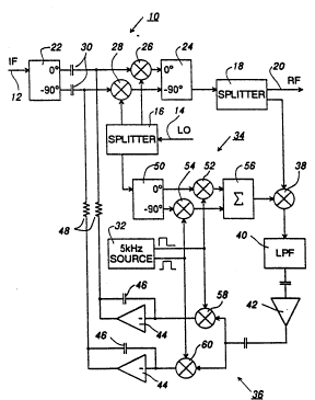
Referring to the drawing, the frequency converter comprises a double balanced
image reject mixer 10 which is supplied with an ~ (intermediate frequency) signal OD aD
IF input line 12 and with an LO (local oscillator) signal via an LO input line 14 and a
splitter 16, and which produces an upper sideband RF (radio frequency) signal which is
20 eoupled via a splitter 18 to an RF output line 20. For example the frequencies of the IF
- and LO signals may be of the order of 140MHz and 4GHz respeetively.
The image rejeet mixer 10 is of genelally known form, comprising two phase
quadrature hy~rid eouplers 22 and 24 and two mixers 26 and 28. The IF signal is
supplied, at a low level for linear operation of the image rejeet mixer, from ~e line 12 to
25 an input of the coupler 22, whose phase quadrature (0 and -90) outputs are eoupled, via
capacitors 30 for d.c. isolation, to signal ports of the mixers 26 and 28 respectivdy.
Local osciLlator porls of these n~ixers 26 and 28 are supplied vnth the LO signa1, at a
relativdy high levd, from the splitter 16, and outputs of these rnixers are eoup1ed to phase
quad~ature (0 and -90) inputs of the coupler 24, whose output is eoupled to the splitter
30 18 and hence to the RF output line 20.
As already described above, especially in view of the relatively higb levd of the
LO sigr~, a earrier leak, or signal eomponent at the LO or ealTier frequeney, can occur at
the outplt of the image reject mixer 10 due to imperfeet balanee, and must be removed
before amplification of thc RF signal. In this embodiment of the inveDtioQ, t~is canier
35 leakis substantially completcly removedby feedback compensation ornullingas
describcd below, so that thac is no need for a subsequent C~UTier frequency filter.
Accordin~py, ~e feedback circuitly described below is refcrrcd to as nulling circuitry,
WO 91/lX44' PCI/CA91/0015]
29~9~04
because it serves to null the carrier leak, or reduce it substantially, so that it is removed
from the signai on the RF output line 20.
The nulling circuitry is chopper stabilised by a SkHz chopper signal source 32
which produces at its outputs two 5kHz square waves which are in phase quadrature, i.e.
5 whose waveforms are offset in time by one quarter of a period of the square wave, in
order to achieve a high isolation between phase quadrature signal components. The
drawing illustrates, adjacent the respective outputs of the source 32, the relative timing of
the waveforms at these outputs. These chopper signals are supplied to a cross or 4-phase
modulator 34 and to a cross demodulator 36 which for n part of the nulling circuitry. The
10 nulling circuitry also comprises a single-ended mixer 38, a low pass filter (LPF) 40, a
capacitively coupled amplifier 42, and two integ~ing arnplifiers 44 each of which
includes a negative feedback integrating capacitor 46 and an output coupling resistor 48.
The 4-phase modulator 34 comprises a quadrature hybrid coupler S0, two mixers
52 and 54, and a summing circuit 56. A portion of the LO signal on the 1ine 14 is
15 supplied via the splitter 16 to an input of the coupler 50, whose phase quadrature (0 and
-90) outputs are coupled to signal ports of the mixers 52 and 54 respectively. Local
oscillator ports of these mixers 52 and 54 are supplied with the phase quadrature chopper
signals from the source 32, and outputs of these mixers are summed by the summing
circuit 56, whose output is coupled to a local oscillator port of the sin~le-ended mixer 38.
20 A small portion of the RF si~a1 is supplied to a signal port of the single-ended rnixer 38
from the splitter 18.
The output of the single-ended mixer 38 is supplied to the LPF 40, which has a
bandwidth of the order of 401~Hz and hence sufficient to pass the Sl& square vaveform
of the chopper signals. The output of this filter 40 is amplified by the amplifier 42 and
25 supplied to signal ports of two mixers 58 and 60, which constitute the cross demodulator
36 and whose local oscillator por~s are supplied v~ith the phasc quadrature chopper
signals, respectively. Output signals of these rnLlcels 58 and 60 are integrated by the
integlating amplifiers 44 to produce d.c. offset signals which are coupled via the resistors
48 to the phase quadrature patbs, respectively, of the image reject mixer 10 between the
30 capacitors 30 and the signal ports of the mixers 26 and 28.
In operation, although the mixer 38 is sin81e-ended it providcs a quadrature, ora bitrary phase,`output be~wse it is supplied with quad~ure or arbitIary phase signals at
its signal and loca1 c6ciLlatorpons. Further nore, this mixer 38, togetherwith the low
pass filter40 and the amplifier42, opaates in a chopper-stabilised loop between thc
35 4-phase modulator 34 and the cross demodulator 36. Consoquently, thesc parts of the
nulling circuitry sene to monitor arbitra~y phases of carrier leal~ at the output of the irnage
r~ject mi~er 10.
wo 9 1 / 1 844~ PCT/CA9 t /0015 1
2 ~ 6 91 ~
The phase quadsture outputs of the mixers 58 and 60 are integrated and fed back
as d.c. offset signals to the image reject mixer phasle quadrature paths, as described
above, in order to compensate for and hence null such arbitrary phase carrier leak. The
time constant of the integsting amplifiers 44 can be rela ively large, as the carrier leak for
5 any particular image reject mixer is not subject to rapid cbange.
A frequency converter as described above, using a single-ended mixer 38 and
choppper stabilisation, has been found to achieve a reduction in carrier 1eak in the RF
output signal of about 65 to 70dB. This is su~ficient to avoid the need for, and costs of,
using either a subsequent high quality carrier frequency fi1ter or a phase quadrature mixer
10 in place of the single-ended mixer 38.
Although the embodiment of the invention described abovc relates to a particularconfigustion and particular frequencies, it should be appreciated that the invention is
applicable to frequency converters geneslly, and that numerous modifications, variations,
andadaptatiorsmaybemade.
.:
.
: