Language selection

Search

Patent 2077486 Summary

Third-party information liability

Some of the information on this Web page has been provided by external sources. The Government of Canada is not responsible for the accuracy, reliability or currency of the information supplied by external sources. Users wishing to rely upon this information should consult directly with the source of the information. Content provided by external sources is not subject to official languages, privacy and accessibility requirements.

Claims and Abstract availability

Any discrepancies in the text and image of the Claims and Abstract are due to differing posting times. Text of the Claims and Abstract are posted:

  • At the time the application is open to public inspection;
  • At the time of issue of the patent (grant).
(12) Patent: (11) CA 2077486
(54) English Title: ELECTRICAL CONNECTOR CIRCUIT WAFER
(54) French Title: GALETTE A SEMI-CONDUCTEUR DE TYPE CONNECTEUR ELECTRIQUE
Status: Expired
Bibliographic Data
(51) International Patent Classification (IPC):
  • H01R 13/66 (2006.01)
  • G06F 1/00 (2006.01)
  • H01L 23/525 (2006.01)
  • H01R 13/639 (2006.01)
  • H01R 33/74 (2006.01)
  • H02J 7/00 (2006.01)
  • H05K 1/02 (2006.01)
  • H01R 9/03 (2006.01)
  • H05K 1/18 (2006.01)
(72) Inventors :
  • FOREMAN, KEVIN GALE (United States of America)
  • MILLER, PAUL JAY (United States of America)
(73) Owners :
  • TRW INC. (United States of America)
(71) Applicants :
(74) Agent: GOWLING LAFLEUR HENDERSON LLP
(74) Associate agent:
(45) Issued: 1995-09-26
(22) Filed Date: 1992-09-03
(41) Open to Public Inspection: 1993-12-06
Examination requested: 1993-02-11
Availability of licence: N/A
(25) Language of filing: English

Patent Cooperation Treaty (PCT): No

(30) Application Priority Data:
Application No. Country/Territory Date
895,148 United States of America 1992-06-05

Abstracts

English Abstract


A semiconductor wafer has a plurality of holes
therein which correspond to pins of an electrical
connector. The wafer includes circuitry thereon and
contacts for making electrical connection to the pins. In
such manner, the circuitry on the wafer can be used for a
wide variety of purposes such as testing or modifying
signals carried by the pins. The wafer can be installed
in any common electrical connector pair without prior
modification or preparation of the connectors and without
impairing the normal fit or function of the mated
connector pair.


Claims

Note: Claims are shown in the official language in which they were submitted.


13

CLAIMS

What is Claimed is:
1. A device for making electrical connection to a
plurality of pins in a male connector which mates with
sockets in a female connector, said device comprising:
a wafer having a series of holes therein aligned
with the pins in the male connector, said wafer being
insertable into the male connector so that the pins extend
through the holes;
circuit means on the wafer for using electrical
signals on the pins; and
contact means for making electrical contact
between the pins as they extend through the holes in the
wafer and the circuit means.


2. The device of Claim 1 wherein said wafer is made
of semiconductor material.

3. The device of Claim 2 wherein said circuit means
comprises an integrated circuit formed in the
semiconductor wafer.


4. The device of Claim 2 wherein said circuit means
comprises:
means on the semiconductor wafer for defining at
least one fuse coupled to the contact means, with the fuse


14

melting when a signal on a pin exceeds a preselected
level.

5. The device of Claim 1 wherein the connectors
each include a metallic shell, and wherein the device
further comprises:
second contact means for making removable
electrical connection between the wafer and one of the
shells.

6. The device of Claim 1 which further comprises:
communication means for receiving and
transmitting information between the circuit means on the
wafer and a remote controller.

7. The device of Claim 6 wherein the communication
means comprises:
optical transceiver means on the wafer;
remote optical transceiver means spaced from the
connectors; and
light waveguide means for transmitting optical
signals between the transceiver on the wafer and the
remote transceiver.


8. The device of Claim 7 wherein the light
waveguide means comprises:
a flexible strip extending between shells of the
male and female connectors, one end of the strip being
connected to the transceiver on the wafer, and another end
of the strip being connected to the remote transceiver.

9. The device of Claim 1 wherein said contact means
comprises:
metallic discs each having a plurality of
inwardly extending bendable fingers terminating at an
aperture in the disc, outer rim portions of each disc
being connected to the wafer so that the apertures in the
disc aligns with a hole in the wafer, and wherein the pins
extend through the apertures and the bendable fingers make
electrical connection between the pins and the wafer.


16
10. The combination comprising:
a male electrical connector having an outer
metallic shell and a plurality of electrically conductive
pins carrying electrical signals to electronic equipment;
a male connector having an outer metallic shell
and a plurality of sockets for receiving the pins in the
male connector; and
a semiconductor wafer lying between the male and
female connectors, the wafer being sufficiently thin to
permit the male and female connectors to be mated together
to permit the pins to engage the sockets, the wafer
including contact means for making removable electrical
connection between the pins and the wafer to thereby
permit the wafer to be inserted and removed from the
interior of the shell of the male connector; and circuit
means on the wafer for electrically communicating through
the contact means with the pins on the male connector;
whereby the wafer provides simple electrical
connection to the pins and to the electronic equipment
coupled thereto.

11. The combination of Claim 10 wherein said circuit
means comprises an integrated circuit formed on the
semiconductor wafer.


17
12. The combination of Claim 10 wherein said circuit
means comprises:
means on the semiconductor wafer for defining at
least one fuse coupled to the contact means, with the fuse
melting when a signal on the pin exceeds a preselected
level.

13. The combination of Claim 10 which further
comprises:
second contact means for making removable
electrical connection between the wafer and one of the
shells.

14. The combination of Claim 10 which further
comprises:
bidirectional communication means for receiving
and transmitting information between the circuit means on
the wafer and a remote controller.

15. The combination of Claim 14 wherein the
bidirectional communication means comprises:
optical transceiver means on the wafer;
remote optical transceiver means spaced from the
connectors; and
light waveguide means for transmitting optical
signals between the transceiver on the wafer and the
remote transceiver.


18
16. The combination of Claim 15 wherein the light
waveguide means comprises:
a flexible strip extending between the shells of
the male and female connectors, one end of the strip being
connected to the transceiver on the wafer, and another end
of the strip being connected to the remote transceiver.

17. The combination of Claim 10 wherein said contact
means comprises:
metallic discs each having a plurality of
inwardly extending bendable fingers terminating at an
aperture in the disc, outer peripheral portions of each
disc being connected to the wafer so that the aperture in
the disc aligns with a hole in the wafer, and wherein the
pin extends through the apertures and the bendable fingers
make electrical connection between the pins and the wafer.


19
18. A method of making electrical connection to
electronic equipment that is removably connected to an
electrical cable by mating male and female connectors, the
male connector having a plurality of pins extending into
sockets in the female connector, said method comprising:
providing a wafer having a series of holes
therein corresponding to the pins in the male connector;
inserting the wafer into the male connector so
that the pins extend through the holes in the wafer;
making a wiping electrical contact between the
pins and the wafer; and
using circuitry on the wafer to perform
preselected functions on signals carried by the pins.

19. The method of Claim 18 wherein the method
further comprises:
bidirectionally communicating between the
electronic equipment and a remote controller through the
wafer and its contacts with the pins.

20. The method of Claim 18 which further comprises:
unmating the male and female connectors;
removing the wafer from the male connector; and
measuring characteristics of the circuitry on
the wafer.


21. A device for making electrical connection to a
plurality of pins in a male connector which mates with
sockets in a female receptacle, said device comprising:
a wafer having a series of holes therein aligned
with the pins in the male connector, said wafer being
insertable onto the male connector so that the pins extend
through the holes;
circuit means on the wafer for detecting
electrical signals on the pins;
contact means for making electrical contact
between the pins as they extend through the holes in the
wafer and the circuit means; and
said wafer being sufficiently thin to allow the
male connector to mate with the female receptacle and
permit the circuit means to detect electrical signals
flowing between the female sockets and male connector pins.

22. The device of claim 21 wherein said wafer is made
of semiconductor material.

23. The device of claim 22 wherein said circuit means
comprises an integrated circuit formed in the semiconductor
wafer.
24. The device of claim 22 wherein said circuit means
comprises:


21
means on the semiconductor wafer for defining at
least one fuse coupled to the contact means, with the fuse
melting when a signal on a pin exceeds a preselected level.

25. The device of claim 21 wherein the male connector
includes a metallic shell, and wherein the device further
comprises:
second contact means for making removable
electrical connection between the wafer and the shell.

26. The device of claim 21 which further comprises:
communication means for transmitting information
from the circuit means on the wafer to a remote controller.

27. The device of claim 26 wherein the communication
means comprises:
optical transmitter means on the wafer;
remote optical receiver means spaced from the
wafer; and
light waveguide means for transmitting optical
signals from the transmitter on the wafer to the remote
receiver.

28. The device of claim 27 wherein the male connector
is a cable connector having an outer shell and wherein the
female receptacle comprises a female cable connector with
an outer shell that is removably connected to the shell of
the male connector.


22
29. The device of claim 28 wherein the light
waveguide means comprises:
a flexible strip extending between the shells of
the male and female connectors, one end of the strip being
connected to the transmitter on the wafer, and another end
of the strip being connected to the remote receiver.

30. The device of claim 21 wherein said contact means
comprises:
metallic discs each having a plurality of
inwardly extending bendable fingers terminating at an
aperture in the disc, outer rim portions of each disc being
connected to the wafer so that the apertures in the disc
aligns with a hole in the wafer, and wherein the pins
extend through the apertures and the bendable fingers make
electrical connection between the pins and the wafer.

31. The device of claim 21 wherein said circuit means
comprises means for detecting characteristics of the power
of the electrical signals flowing between the female
receptacle and the male connector.

32. A method of detecting characteristics of
electrical signals flowing between a male connector that is
removably connected to a female receptacle, the male
connector having a plurality of pins extending into sockets
in the female receptacle, said method comprising:


23

providing a wafer having a series of holes
therein corresponding to the pins in the male connector;
inserting the wafer into the male connector so
that the pins extend through the holes in the wafer;
making electrical contact between the pins and
circuitry on the wafer;
mating the male connector and the female
receptacle, with the wafer being sandwiched therebetween;
and
using the circuitry on the wafer to perform
preselected functions on signals carried by the pins.

33. The method of claim 32 which further comprises:
unmating the male connector and female
receptacle;
removing the wafer from the male connector; and
detecting characteristics of the circuitry on the
wafer.

34. The method of claim 33 wherein said circuitry
senses power flowing between the female receptacle and male
connector, and wherein said detecting step tests for
characteristics of power as sensed by the circuitry.


Description

Note: Descriptions are shown in the official language in which they were submitted.


ELECTRICAL CONNECTO~ CIRCUIT WAFER 2 0 7 7 4 8

BACKGRO~ND OF THE l~v~NllON
1. Technical Field
This invention relates to electronic components and,
more particularly, to a device for making electrical
connection to a plurality of pins in a male connector.

2. Discussion
Electrical connections and cables are used in a
variety of applications to transmit electrical signals
from different sources to an equally wide variety of
destinations. The cables generally include a plurality of
individual wires which terminate at one end in either a
male connector or a female connector. The male connector
typically employs a series of pins which are housed in a
generally cylindrical or rectangular shell that mate with
sockets in the female connector.
It sometimes becomes necessary or desirable to obtain
access to the electrical signals carried by each of the
individual cable wires. For example, it may be desirable
to detect the peak level of electromagnetic pulse induced
stress on all of the pins. In the past, a complex array
of passive and active instrumentation components was
required to perform such tests. Much of the complexity is
due to the fact that there is no convenient way to obtain
access to the signals carried by the individual wires in
the cable.

2 2077Q~
- It is also envisioned that there exists a need to
provide a relatively simple, yet reliable technique for
easily coupling electrical circuits to the pins in such
connectors. The electrical circuits could consist of
active or passive electronic components, as well as more
sophisticated microprocessors. Despite this need, it does
not appear that the prior art has proposed an eloquently
simple solution to the problem in the manner suggested by
the present invention.
8~MMARY OF TRE lNv~h~lON
In accordance with the teachings of the present
invention, a wafer, preferably of semiconductor material,
is provided that has a series of holes in it that are
aligned with the pins in the male connector. The wafer is
inserted into the male connector so that the pins pass
through the holes in the wafer. The wafer contains any
of a wide variety of circuit means for performing
preselected functions associated with the signals on the
pins. These circuit means can include passive or active
electronic components, or the aforementioned
microprocessor circuits which are easily implemented in
integrated circuit form on the wafer. The wafer further
includes contact means for making electrical contact
between the pins as they extend through the holes in the
wafer and the circuit means. In such manner, electrical
connection between the desired circuit and the pins in the
connector is easily and rapidly made, without requiring

3 2077~8~
- advance preparations of the host connector pair. As will
appear, the present invention has a wide variety of
applications.

BRIEF DESCRIPTION OF TRE DRAWING8
The various advantages of the present invention will
become apparent to those skilled in the art after a study
of the specification and by reference to the drawings in
which:
FIG. 1 is an exploded perspective view showing the
installation of a wafer made in accordance with the
teachings of the preferEed embodiment of this invention;
FIG. 2 is a cross-sectional view of one embodiment of
the invention in which the wafer is sandwiched between
mated male and female connectors;
FIG. 3 is a partial cross-sectional view illustrating
another embodiment and one technique for making electrical
contact between the pins and the wafer;
FIG. 4 is a plan view of a suitable contact
configuration;
FIG. 5 is a partial side view showing the contact
design in use;
FIG. 6 is a plan view illustrating one particular
circuit design for the wafer;
FIG. 7 is a side view of the wafer of FIG. 6; and
FIG. 8 is a block diagram view of a system which may
be used to test the wafers.

4 20774~
_ DESCRIPTION OF TRE PREFERRED EMBODI~ENTS
It should be understood from the outset that the
present invention will be described in connection with a
few limited examples which illustrate the best mode of
practicing the invention at the time that this application
was filed. However, various modifications will become
apparent to those skilled in the art after having the
benefit of studying the text, drawings and claims which
follow this detailed specification. With that caveat in
mind, the attention of the reader should now be turned to
the drawings, especially FIG. 1.
In accordance with the preferred teachings of this
invention, a wafer 10 is provided for making electrical
connection to the pins 12 of a male electrical connector
14. Male electrical connector 14 mates with a female
connector 16 in a manner well known in the art. By way of
a specific, although not limiting example, and as shown in
more detail in FIGS. 2-3, the male/female connectors 14
and 16 are of the type meeting military specification (C-
38999). The male connector is characterized by a
cylindrical metal outer shell which is removably connected
to a complementary metal shell 20 on the female connector
16. The removable connection is usually made by a bayonet
coupling on the mating surfaces of the shells 18 and 20,
although other such connections can also be made to ensure
proper mating of the connectors.
The interior of the male connector includes a
nonconductive insert 2Z that maintains the orientation of

5 207748~
~ the pins 12 and insulates them from the conductive shell
18. The female connector 16 likewise includes a
nonconductive insert 24 and an array of sockets 26 for
receiving the pins 12.
The male connector is shown in FIG. 1 as being
coupled to electronic equipment 28. The female connector
16 is mounted on one end of an electrical cable 30. The
cable contains a plurality of wires that carry electrical
signals to and from the electronic equipment 28 when the
connectors 14 and 16 are mated together.
In accordance with the teachings of this invention,
the wafer 10 is inserted between the mated connectors 14
and 16. The wafer 10 has a diameter smaller than the
inner diameter of the smallest connector shell and is thin
enough to be inserted between the connector pair without
interfering with the positive connection therebetween. As
shown perhaps best in FIG. 3, wafer 10 includes two
generally parallel major surfaces 32 and 34, along with a
peripheral edge 36. A series of holes 38 are formed
between the two major faces of the wafer. Holes 38 are
aligned with and slightly larger than the diameter of pins
12.
Circuitry, generally designated by the numeral 40, is
formed on the wafer 10 and is in electrical contact with
one or more of the pins 12. The circuitry 40 can be any
of a wide variety of devices such as active and passive
electronic components, as well as more sophisticated
microprocessing circuitry. The circuitry 40 is generally

6 2~774~
designed to perform preselected functions associated with
the electrical signals on the pins 12. These functions
include, but are not limited to, radio frequency
instrumentation, signal rerouting and interface protection
using passive electronic components such as
current/voltage monitors, transient limiters and point-to-
point wiring. Active electronics such as analog and logic
circuitry, matrix switches, power management devices and
temperature/shock sensors can be utilized to provide
discrete event monitoring, integrated built-in test
augmentation and diagnostics, signal processing, interface
diagnostics and/or signal conditioning. Circuitry 40, on
the other hand, may take the form of microprocessing
circuitry such as the 68000 variety, and may include
static RAM and ROM as well as non-volatile memory. In
that event, the circuitry can provide discrete event
recordation and decision based signal
conditioning/diagnostics.
Circuitry 40 is shown in FIG. 6, however, as
consisting simply of a plurality of fuses 42(a, b, and c)
which are formed by areas of reduced widths in a thin film
metal layer 42 formed on surface 32 of wafer 10. The
fuses 40(a, b and c) are connected to the pins and
operate, in this example, to sense electromagnetic pulse
induced stress on the pins 12. If, for example, a
potentially damaging pulse is received exceeding a
predetermined current level then one or more of the fuses
will melt causing a change in resistance associated with

7 2077~8~
~ that pin. The wafer, in this example, takes the form of
a silicon substrate 41 and includes a passivation layer
46, as shown in FIG. 7. Instead of the circuitry 40 being
a simple metal fuse formed on the wafer surface,
S conventional very large scale integration circuit
techniques can be used to form active devices within the
body of the semiconductor wafer.
In any event, some type of electrical connection is
also provided between the pins 12 and the circuitry 40.
In this particular example, a metallic disc 50 is provided
for each wafer hole 38. As shown best in FIGS. 3-5, each
metallic disc 50 includes an aperture 52 whose diameter is
slightly smaller than the cross sectional diameter of the
connector pin 12. A plurality of radially extending slits
lS 54 define an array of bendable fingers 56, the inner
portions of which serve to bend under the force of the
connector pin being inserted through the wafer holes 38 to
thereby make a sliding, removable, yet positive electrical
connection with each pin. The non-slitted peripheral rim
58 of the disc 50 is mounted by way of conductive epoxy or
solder to conductive circular pads 60 on wafer 10
surrounding holes 38. The discs 50 are connected by way
of metal traces 42 to the circuitry which, in FIG. 5,
bears the reference numeral 40' to represent an active
electronic integrated circuit component formed in the
surface of semiconductor material serving as wafer 10.
In most applications it is necessary to make
electrical connection to the innermost shell of the

8 2077~8B
~ connector pair which often serves as an electrical ground.
In such instances similar wiping electrically conductive
fingers 62 can be used for this purpose, as seen in FIG.
3.
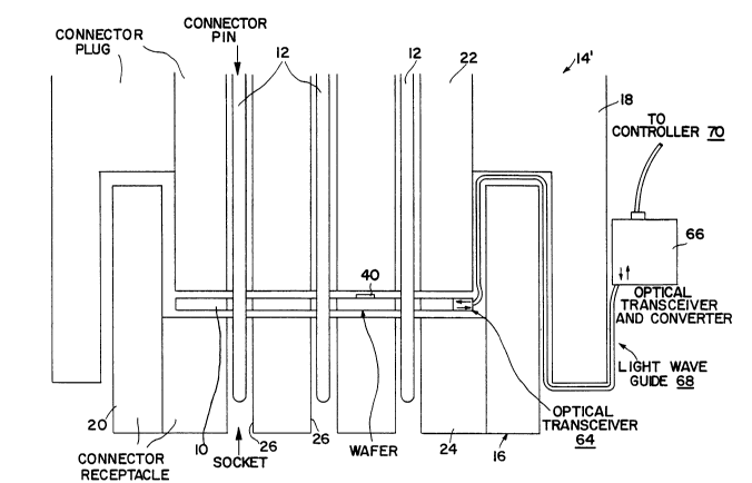
FIG. 2 illustrates a somewhat more sophisticated
embodiment where-bidirectional communication is made
between the circuitry 40 on the wafer 10. In such manner,
it is possible to expand the capabilities of the
invention. As shown in FIG. 2, the wafer includes a
suitable onboard optical transceiver 64 which communicates
with a remote transceiver and converter 66 via a light
waveguide 68. Transceiver and converter 66 is coupled to
a suitable controller 70 which may be provided by way of
a host computer. Electrical signals from the controller
70 are converted by transceiver/converter 66 into suitable
light pulses which are transmitted by waveguide 68 to the
transceiver 64 on wafer 10. The waveguide 68 can be made
of suitable material that has sufficient flexibility and
integrity to transmit the optical information in a
reliable manner. It should be flexible enough so that it
can conform with the relatively small pathways left
between shells 20 and 18 of the mated connectors, as
shown. Waveguide 68 can, for example, take the form of a
Mylar strip which is preferably coated with a reflecting
substance on its outer surfaces to increase the efficiency
of the optical transmission.
Optical transceiver 64 converts the optical signal
from waveguide 68 into suitable electrical signals which

9 207748~
~ are fed to the circuitry 40 on the wafer 10. For example,
the signals could be used to program a suitable integrated
circuit microprocessor which serves as the circuitry 40.
The microprocessor then could communicate with the
electronic equipment 28 via the pins 12 in the male
connector 14 (FIG. 1). Likewise, signals from the
electronic equipment 28 can be communicated to the remote
controller 70 via the pins 12, circuitry 40, optical
transceiver 64, waveguide 68 and optical
transceiver/converter 66. A system of this type can be
used for a variety of applications such as advanced signal
processing, intelligent instrumentation, real-time data
stream monitoring, remotely controlled signal
conditioning, switching and processing; remotely
controlled interface diagnostics, transient data
recordation and the like. Again, these applications are
by way of non-limiting examples. Depending upon the
application and type of circuitry on the wafer 10, it may
be desirable to remove the wafer and test the circuitry
thereon. For example, if the circuitry takes the form of
the fuses shown in FIGS. 6 and 7, it would be desirable to
periodically remove and test the wafer to determine if any
of the fuses 40(a, b, c) had melted due to high levels of
electromagnetic induced current pulses on the pins 12.
FIG. 8 illustrates a suitable test console 70 for this
purpose. Console 70 includes a wafer identification unit
72, a wafer test fixture 74, a switching matrix 76,
measurement circuitry 78, threshold verification circuitry

lO 207748~

- 80 and computer control 82. The identification unit 72
uniquely identifies a wafer 10 by means of an
identification tag 84 on each wafer 10. Tag 84, in this
example, is a conventional bar code which can be read by
a suitable bar code reader 86.
A wafer extraction tool 88 aids in the insertion and
removal of the wafer into the connector 14 and ~in;mizes
the risk of wafer damage due to mechanical stress or other
events. Tool 88 employs a vacuum system 90 with a vacuum
head 92 designed to temporarily hold the wafer 10. During
insertion, the head 92 manipulates the wafer so that the
pins slide into the wafer holes 38 and make electrical
connection to the pin contacts 50 and the shell contacts
62 make connection to the shell 18 (FIG. 3). The male and
female connectors 14 and 16 are then mated together in the
usual manner with the pins 12 being inserted into the
female sockets 26. As illustrated in the drawings, the
wafer 10 is sufficiently thin that it does not disturb the
normal mating of the connectors. To remove the wafer 10,
the connectors are disassembled and the vacuum tool 88 is
used to extract the wafer 10 from the male connector 14.
The wafers then are placed in the test fixture 74
which generally consists of a bank of the same MIL-SPEC
connectors 14. The test fixture 74 is capable of testing
one wafer at a time by placing the wafer in its
corresponding connector. An LED indicator 94
automatically locates the proper connector to use based on
the wafer's identification code. The switching matrix 76

207748~
11 ,
switches the resistance measurement between any pin on the
connector and another pin or the connector shell. It also
switches in an onboard switched DC power supply to verify
the threshold of any of the fuses 40(a, b or c). The
switching matrix 76 is controlled by the computer 82
through a bus interface card. The measurement circuitry
78 makes a resistance measurement that determines which
fuses 40(a, b or c), if any, have been blown. An A/D
converter with a fast sampling rate is used so that many
fuses can be tested in a small amount of time. The
threshold verification circuitry 80 includes a
programmable switch DC power supply and a source resistant
network. It creates a known square pulse with enough
amplitude to blow any of the fuses. The pulse level is
stepped up slowly and the fuse resistance is read after
each pulse to determine when the fuse blows and what its
threshold was. Computer control 82 controls all of the
systems and records the data from the test. The computer
is suitably programmed so that it will control all the
testing procedure.
From the foregoing, those skilled in the art should
realize that the present invention provides a simple, yet
reliable way to rapidly and unintrusively make electrical
connection to pins in electrical connectors and which
further enables the user to modify or add a wide variety
of functions through the use of the appropriate circuitry
on the wafer. As noted from the outset, the invention has
been described in connection with a few particular

12 2077 4~6
- examples. However, various modifications and other
applications will become apparent to the skilled
practitioner after having the benefit of studying the
specification, drawings and following claims.


Representative Drawing
A single figure which represents the drawing illustrating the invention.
Administrative Status

For a clearer understanding of the status of the application/patent presented on this page, the site Disclaimer , as well as the definitions for Patent , Administrative Status , Maintenance Fee  and Payment History  should be consulted.

Administrative Status

Title Date
Forecasted Issue Date 1995-09-26
(22) Filed 1992-09-03
Examination Requested 1993-02-11
(41) Open to Public Inspection 1993-12-06
(45) Issued 1995-09-26
Expired 2012-09-04

Abandonment History

There is no abandonment history.

Payment History

Fee Type Anniversary Year Due Date Amount Paid Paid Date
Application Fee $0.00 1992-09-03
Registration of a document - section 124 $0.00 1993-03-30
Maintenance Fee - Application - New Act 2 1994-09-05 $100.00 1994-07-25
Maintenance Fee - Application - New Act 3 1995-09-04 $100.00 1995-03-24
Maintenance Fee - Patent - New Act 4 1996-09-03 $100.00 1996-08-19
Maintenance Fee - Patent - New Act 5 1997-09-03 $150.00 1997-08-13
Maintenance Fee - Patent - New Act 6 1998-09-03 $150.00 1998-08-04
Maintenance Fee - Patent - New Act 7 1999-09-03 $150.00 1999-08-09
Maintenance Fee - Patent - New Act 8 2000-09-04 $150.00 2000-08-08
Maintenance Fee - Patent - New Act 9 2001-09-03 $150.00 2001-08-07
Maintenance Fee - Patent - New Act 10 2002-09-03 $200.00 2002-08-08
Maintenance Fee - Patent - New Act 11 2003-09-03 $200.00 2003-08-21
Maintenance Fee - Patent - New Act 12 2004-09-03 $250.00 2004-08-20
Maintenance Fee - Patent - New Act 13 2005-09-06 $250.00 2005-08-19
Maintenance Fee - Patent - New Act 14 2006-09-05 $250.00 2006-08-17
Maintenance Fee - Patent - New Act 15 2007-09-04 $450.00 2007-08-17
Maintenance Fee - Patent - New Act 16 2008-09-03 $450.00 2008-08-25
Maintenance Fee - Patent - New Act 17 2009-09-03 $450.00 2009-08-21
Maintenance Fee - Patent - New Act 18 2010-09-03 $450.00 2010-08-19
Maintenance Fee - Patent - New Act 19 2011-09-05 $450.00 2011-08-18
Owners on Record

Note: Records showing the ownership history in alphabetical order.

Current Owners on Record
TRW INC.
Past Owners on Record
FOREMAN, KEVIN GALE
MILLER, PAUL JAY
Past Owners that do not appear in the "Owners on Record" listing will appear in other documentation within the application.
Documents

To view selected files, please enter reCAPTCHA code :


To view images, click a link in the Document Description column. To download the documents, select one or more checkboxes in the first column and then click the "Download Selected in PDF format (Zip Archive)" or the "Download Selected as Single PDF" button.

List of published and non-published patent-specific documents on the CPD .

If you have any difficulty accessing content, you can call the Client Service Centre at 1-866-997-1936 or send them an e-mail at CIPO Client Service Centre.


Document
Description 
Date
(yyyy-mm-dd) 
Number of pages   Size of Image (KB) 
Abstract 1995-09-26 1 18
Description 1995-09-26 12 425
Claims 1995-09-26 11 289
Drawings 1995-09-26 6 127
Representative Drawing 1999-05-13 1 18
Cover Page 1995-09-26 1 16
Abstract 1995-09-26 1 18
PCT Correspondence 1995-07-18 1 42
Office Letter 1993-05-19 1 45
Prosecution Correspondence 1993-02-11 1 33
Prosecution Correspondence 1993-08-31 1 40
Prosecution Correspondence 1993-01-19 5 180
Fees 1995-03-24 2 155
Fees 1996-08-19 1 71
Fees 1994-07-25 1 36