Note: Descriptions are shown in the official language in which they were submitted.
20836~
DIGITAL SIGNAL HARDWARE PROTECTION SWITCHING
Technical Field
This invention relates to tran~mi~sion of digital signals and, more
particularly, to hardware protection switching.
5 Back~round of the Invention
It has been the practice to duplicate individual hardware units used in
the switching or tr~n~mi~sion of digital signals if failure of a single hardware unit
could cause the failure of a pledc~c.l,lined number of digital signal ch~nn~ . That
is, there must be a backup haldw~ unit which can be switched to in the event of
10 such a hal.lwalc unit failure. In known hardware protection switching arrangements,
the swi~cl~ing of digital signals from one ha~lw~ unit to the other is achieved by
employing relays. In such arran~ ents, signal loss is detected and the signal isredirected to a standby unit. A problem with the relay switching arrangement is that
the customer co..-.~-...-i~ation traffic is inLcllupted for a ~ignifi~nt interval. This
15 interruption could cause calls to be dropped, which is undesirable. Even if the call is
not dropped, the relay switching causes so-called glitches or hits in the digital signal
tr~n~mitting the customer cv.. l.l-ic~tion~ traffic which may cause an alarm
cnn-lition For example, the glitch could propagate as a bipolar violadon or the like.
Summary of the Invention
The problems of prior hal.lware protecdon switching arr~ngem~nts are
O~vC~Cvll~ in accol~lce with the invendon, by employing ha,dw~e units including
~wi~ching units which can individually determine the instant to switch from an active
state to a standby state and vice versa in order to achieve a so-called "hitless" switch
of the ha~dware unit supplying a digital signal to and receiving a digital signal from
25 a transmission line.
In one embodiment, the desired hitless switching of h~dwale units is
realized by assuring that timing signals supplied to each of the hardware units, i.e.,
active and associated standby, are phase aligned and by initi~li7ing a switching unit
in a first hardware unit into an active state and an associated switching unit in a
30 second hardware unit into a standby state. To initiate a haldwale protection switch, a
protection switch request signal is supplied to the switching unit in the current active
hardware unit. The active switching unit determines if a data bit to be supplied as an
output resulting from a current input data bit has a prescribed bit condition. If the
prescribed bit condition is detected, a first control signal, e.g., a prescribed
- 2 -
synchronization pulse, is supplied from the current active switching unit to the associated
standby switching unit. In response to the prescribed synchronization pulse, the bit
condition of the digital signal to be supplied as an output from the standby switching unit,
5 resulting from the current input bit, is caused to be aligned with the bit condition of the
digital signal being supplied as an output from the current active switching unit. Then,
output circuits in the current active switching unit and in the standby switching unit must
be simultaneously turned OFF and ON, respectively. This is achieved by the switching
units individually observing the common digital data signal being supplied as an input to
10 them. Upon detection by each of the switching units of a prescribed bit condition of the
common input digital signal, a second control signal is generated which causes the output
circuit in the current active hardware switching unit to be turned OFF and the output
circuit in the standby hardware switching unit to be turned ON at the same instant. Again,
the instant that the output circuits are turned OFF and ON is determined individually in
15 each hardware switching unit. Consequently, the prior standby hardware switching unit
is now the active unit and the prior active hardware switching unit is now the standby
unit.
A technical advantage of the invention is that no central switching control unitis needed to determine the instant when to switch from an active hardware unit to a
20 standby hardware unit. Control apparatus is employed only to initiate the hardware unit
switch.
In accordance with one aspect of the present invention there is provided a
protection switching unit for use in a hardware protection switching arrangement for
controllably supplying and receiving a digital signal to and from, respectively, a digital
25 transmission line, the protection switching unit comprising: means for multiplexing a
digital data signal into a prescribed digital signal having a predetermined framing format;
means responsive to a switch request signal for detecting a next bit having a first
predetermined bit condition of a digital signal being supplied as an output from the unit;
means for generating a first control signal in response to said means for detecting
30 indicating that a bit having said ~Irst predeterrnined bit condition has been detected of said
digital signal being supplied as an output from the unit; means for supplying said first
control signal as an output from the unit; means responsive to a received first control
r~
l~
~ ~ ~ 3 ~ ~ ~
- 2a -
signal for synchronizing to said first predetermined bit condition of a digital signal to be
supplied as an output from the unit to the digital transmission line; means for generating
a second control signal based on a second predetermined bit condition of a digital signal
5 being supplied as an input to the unit; and output circuit means for supplying an output
to the digital transmission line, said output circuit means having an ON state and an OFF
state and being responsive to said second control signal to select either the ON state or
the OFF state.
In accordance with another aspect of the present invention there is provided a
10 method for hardware protection switching of apparatus for supplying and receiving a
digital signal to and from, respectively, a digital transmission line, comprising the steps
of: multiplexing a digital data signal into a prescribed digital signal having apredetermined framing format; in response to a switch initiation signal detecting a next
bit having a first predetermined bit condition of a digital signal being supplied as an
15 output from the unit; generating a first control signal indicative that said first
predetermined bit condition has been detected; supplying said first control signal as an
output from the apparatus; in response to a received first control signal, synchronizing to
said first predetermined bit condition of a digital signal to be supplied as an output from
the apparatus; detecting a second predetermined bit condition of a digital signal being
20 supplied as an input to the apparatus; generating a second control signal indicative that
said second bit condition has been detected; and in response to said second control signal,
enabling or disabling supplying an output from the apparatus to the digital transmission
hne.
Brief Description of the Drawin~
25 In the drawings:
FIGs. I through 4 when connected as shown in FIG. 5 show, in simplified block
diagram form, a system employing a hardware protection switching arrangement including
an embodiment of the invention;
FIG. 6 shows, in simplified block diagram form, details of digital signal
30 interface-switch (DSI-S) units 1 12;
FIG. 7 shows, in flow chart form, details of the operation of DSI-S units 112
when in an active state; and
FIG. 8 shows, in flow chart form, details of the operation of DSI-S units 112
when in a standby state.
2Q~3fi35
Detailed Description
FIGs. 1 through 4 when connected as shown in FIG. S show, in
simplified block diagram form, a system employing a hidess hal.lw~ protection
switching arrangement, in~ ing an embodiment of the invention. Specifically,
5 shown are data transmit, receive and control unit 101, interface units 104(1) and
104(0), h~dw~e units 105(1) and 105(0) and line coupler unit 106. The
designations "(l)" and "(0)" are used to denote appalalus associated with, for
example, an active h~.lw~ unit (1) and its associated standby haldwan~ unit (0).Data transmit, receive and control unit 101 is, for example, a digital switch, digital
10 access and cross-connect system, intelligent multiplexer or the like and,
illustratively, is a SESS~ digital switch co",.,le.cially available from AT&T.
Hereinafter, data transrnit, receive and control unit 101 is referred to as digital switch
101. Although only two haldwa~ units 105(1) and 105(0) are shown in this
example, it will be apparent that any number of hardware unit pairs, i.e., active (1)
15 and standby (0), may be employed as desired with a particular digital switch 101.
Digital switch 101 supplies and l~C~iVes control infolmation to and from
interfaces 104(1) and 104(0) via control buses 102(1) and 102(0), respectively. The
control information includes, but is not limited to the digital signal format to be used
by hardwale units 105(1) and 105(0), whether a hardware protection switch is to be
20 initiated and whether a hardware protection switch has been completed. Digital
switch 101 also supplies to and receives from interfaces 104(1) and 104(0) digital
data signals via data buses 103(1) and 103(0), respectively. In this example, buses
103(1) and 103(0) are each the known peripheral interface data bus (PIDB) used in
the SESS~) digital switch. The individual digital data signals being supplied to and
25 from interfaces 104 via the PIDB buses 103 are, in this example, unipolar. The
digital data signals being supplied on data buses 103 include N digital data signals,
which are supplied in multiplexed fashion.
Interface units 104(1) and 104(0) are also employed to supply and
receive control information, and the N digital data signals to and from hardware30 units 105(1) and 105(0), respectively. Additionally, interface units 104(1) and
104(0) also supply timing signals to hardware units 105(1) and 105(0), namely,
TCLOCK (line clock), FSYNC (frame sync) and ESFSYNC (extended super frame
sync). In this example, TCLOCK has a bit rate of 1.544 Mb/sec, FSYNC is suppliedat 8 kHz and ESFSYNC is supplied at 0.3333 kHz, these rates being associated with
35 the well known DS 1 ESF digital signal format. Such timing signals are generated in
well known fashion. Processor 110(1) in hardware unit 105(1) receives and
20~363~
transmits control infolll,adon over bus 120(1) from and to interface 104(1),
respectively. Similarly, processor 110(0) in hardware unit 105(0) receives and
transmits control inrolmation over bus 120(0) from and to interface 104(0),
respectively.
In this example, not to be construed as limiting the scope of the
invention, line coupler unit 106 incl~lcles a first plurality of transformers 116-N
through 116-N and a second plurality of transrollllel~ 117-1 through 117-N for
interfacing to receive portions of a plurality of digital tr~n.~mi~sion lines comprised
of Tl-l and Rl-l through Tl-N and Rl-N and to a plurality of transmit
10 portions of the plurality digital tr~n~mi~ion lines comprised of T2 - 1 and R2 - 1
through T2 - 1 and R2--N, respectively. Thus, in-oming digital signals are supplied
from incoming digital tr~n~mi~ion line portions Tl-l and Rl-l through Tl-N
and Rl-N via ~ rolme.~ 116-1 through 116-N of line coupler 106 to digital
signal interf~ee switch (DSI-S) units 112(1)-1 through 112(1)-N and DSI-S units
15 112(0)-1 through 112(0)-N in hal.lwal~ units 105(1) and 105(0), respectively.Outgoing digital signals are supplied from DSI-S units 112(1)-1 through 112(1)-NandDSI-S units 112(0)-1 through 112(0)-Nviatran~rulllle.~ 117-1 through 117-Nof
line coupler 106 to transmit portions T2- 1 and R2 - 1 through T2 -N and R2-N,
respectively, of the a~soci~t~l N digital tr~n~mi~sion lines. Obviously, outgoing
20 digital signals are only supplied from the active DSI-S 112 units. It is also noted that
such line coupler units are well known in the art and only a simplified version is
shown.
Since h~dw~e units 105(1) and 105(0) are identical, only hardware unit
105(1) will be described in detail. However, it is important to note that the digital
25 data signal T'DATA and timing signals TCLOCK, FSYNC and ESFSYNC supplied
to a PCM transceiver 111(1) in hardware unit 105(1) are il11onti(-~l to the digital data
signal T'DATA and timing signals TCLOCK, FSYNC and ESFSYNC being
supplied to the associated PCM transcei~,er 111(0) in hardware unit 105(0).
Assurance that the timing signals TCLOCK, FSYNC and ESFSYNC are phase
30 aligned is readily obtained by employing a common reference clock signal in known
fashion. The same digital data signal T'DATA is simply supplied to both associated
PCM transceivers 111(1) and 111(0) in the protection swi~ching pair of h~dw~e
units 105(1) and 105(0). These conditions are readily obtained in interface units
104(1) and 104(0). Although the timing signals TCLOCK, FSYNC and ESFSYNC,
35 in this example, are shown as being the same, i.e., in phase alignment, for all of
PCM transceivers 111(1) and 111(0), it is only necessary that the timing signals
2 0t~
being supplied to each pair of PCM transceivers 111(1) and 111(0) be phase aligned.
Specific~lly, h~.lw~e unit 105(1) inclu-les processor 110(1), a plurality
of pulse code mod~ tiQn (PCM) transceivers 111(1)-1 through lll(l)-N and the
afolelllel1tioned plurality of digital signal interface-switch units (DSI-S) 112(1)-1
5 through 112(1)-N. Each of DSI-S units 112(1) receives incoming digital signalsfrom a corresponding digital transmission line via line coupler 106 at inputs T 1 and
Rl, and supplies outgoing digital signals at outputs T2 and R2. As inflicatecl above,
the well known DS 1 ESF digital signal is assumed in this exarnple.
Each of PCM transceivers 111(1)-1 through lll(l)-N receives an
10 associated one of the T'DATA-l through T'DATA-N signals, respectively, and
TCLOCK, FSYNC and ESFSYNC from interf~ce unit 104(1). PCM transceivers
111(1)-1 through lll(l)-N supply received digital data signals R'DATA(l)-l
through R'DATA(l)-N, ~ e~Li~ely, to in~ re unit 104(1). In this example,
T'DATA and R'DATA(l) are unipolar digital data signals including eight (8) bits
15 per time slot. Each of PCM transceivers 111(1)-1 through lll(l)-N formats itsassociated T'DATA digital data signal under control of processor 110(1) into a
form~tted TDATA unipolar DSl ESF digital signal. The form~tted digital signals
TDATA-l through TDATA-N are supplied along with their associated TCLOCK-l
through TCLOCK-N timing signals to the coll~,sponding DSI-S units 112(1)-1
20 through 112(1)-N, respectively. Additionally, each of PCM transceivers 111(1) de-
formats an inroming RDATA unipolar DSl ESF digital signal supplied from the
associated DSI-S unit 112(1) into a digital data signal R'DATA(l) which is supplied
to interf~ce unit 104(1). Processor 110(1) supplies control signals C(l)-l through
C(l)-N to PCM transceivers 111(1)-1 through lll(l)-N, respectively, which in~ic~te
25 the particular PCM digital signal format being employed. Such PCM transceiver arr~ng~ e~-L~ are known and commercially available.
A number of signals are shown as being supplied to and from DSI-S
units 112(1) from and to processor 110(1). In this example, these signals are the
same for each of DSI-S units 112(1). However, in other applications, each of
30 DSI-S units 112(1)-1 through 112(1)-N may have a dirrerent set of such control
signals. Accordingly, the signals are defined as follows without the noted
designations:
MS - Force to active state
SWRQ - Switch initiation signal
2083S~
FSS - Force to standby state
Active state indication signals AS(l)-l through AS(l)-N are supplied from DSI-S
units 112(1)-1 through 112(1)-N, respectively, to processor 110(1). Additionally, a
first control signal, namely, synchronization pulse (SYNCN), is coupled between
S DSI-S units 112(1)-1 through 112(1)-N in hardware unit 105 (1) on a one-to-onebasis to acsoci~tçcl DSI-S units 112(0)-1 through 112(0)-N, l~,~pe~ /ely, in ha,dw&.~
unit 105(0). When either DSI-S unit 112(1) or its ~csoci~tç~ DSI-S unit 112(0) is in
the active state, the corresponding SYNCN connection, i.e., pin, is used as an output.
Conversely, when either DSI-S unit 112(1) or its associated DSI-S unit 112(0) is in
10 the standby state, the col.~;,ponding SYNCN c~ nnection is used as an input.
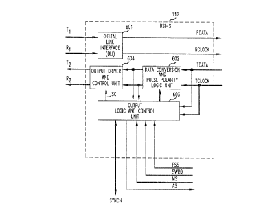
Details of an illustrative one of DSI-S units 112 are shown in FIG. 6, in
simplified block ~ gr~m forrn. Specifically, shown are digital line interface (DLI)
601, data conversion and pulse polarity logic unit 602, output logic and control unit
603 and output driver and control unit 604. A r~,cei~ed digital signal is supplied via
15 Tl and Rl to DLI 601. In this example, as noted above and not to be construed as
limiting the scope of the invention, a DSl ESF digital signal is assumed. The DSl
ESF digital signal is well known in the art and is ~ bipolar signal having three states,
namely, +1, 0 and -1. Digital line interface arrangements, such as DLI 601, are also
well known in the art and usually include among others a bipolar to unipolar
20 converter for obtaining the unipolar RDATA signal from the received DSl ESF
digital signal and timing recovery circuitry for deriving RCLOCK from the received
DSl ESF digital signal. For the DSl ESF digital signal RCLOCK has a bit rate of
1.544 Mb/sec. The RDATA unipolar digital signal and RCLOCK signal are
supplied to the associated PCM transceiver 111 (~;IG. 1).
A TDATA unipolar digital data signal and a corresponding TCLOCK
signal - in this example, the unipolar DSl ESF digital signal and its corresponding
clock signal-are supplied from the associated PCM transceiver 111 to data
conversion and pulse polarity logic unit 602 and to output logic and control unit 603.
Also supplied to output logic and control unit 603 from processor 110 (FIG. 1) are
30 control signals MS, SWRQ and FSS. Output logic and control unit 603 transmits or
receives SYNCN as a first control signal depending on whether the corresponding
DSI-S unit is in the active state or standby state, respectively. Output logic and
control unit 603 also supplies control signal AS to processor 110 and a second
control signal SC to output driver and control unit 604. Control signal AS indicates
35 the state of the DSI- S unit, i.e., active or standby and, therefore, whether or not a
2 0 8 3 ~ ~ ~
switch has been successfully completed. Data conversion and pulse polarity logicunit 602 converts the unipolar TDATA digital signal, in this example, to a bipolar
DS1 ESF digital signal having +1, 0 and -1 bit states, in well known fashion. Data
conversion and pulse polarity logic unit 602 responds to a control signal from output
5 logic and control unit 603 to cause a current bit of the bipolar DS 1 ESF digital signal
to assume a prescribed state in response to a received SYNCN pulse state. In this
example, when a low state, i.e., logical zero (0), SYNCN pulse is received, a bit of
the bipolar DSl ESF digital signal to be supplied as an output resulting from a
current input bit of T'DATA from data conversion and pulse polarity logic unit 602
10 is forced to be in a prescribed con~ition, in this example, a plus one (+1) state. It is
noted that upon l~ceiving the low state SYNCN pulse, the state of the DS1 ESF
digital signal bit being supplied as an output from data convel~ion and pulse polarity
logic unit 602 could be either +1 or -1. The bipolar DSl ESF digital signal output
from data conversion and pulse polarity logic unit 602 and TCLOCK are supplied to
15 output driver and control unit 604 which, in turn, supplies the bipolar DSl ESF
digital signal to the transmit data tr~n~mi~ion line comrri~e~ of T2 and R2. Thebipolar DS 1 ESF digital signal output from data conversion and pulse polarity logic
unit 602 is also supplied to output logic and control unit 603. The output driver
circuit in output driver and control unit 604 includes a semiconductor device (not
20 shown) which in response to first and second states of the aforemelltioned second
control signal SC from output logic and control unit 603 is opc;ld~ e to supply the
bipolar DSl ESF digital signal to T2, R2 when in the active state or to present an
open circuited output to T2, R2 when in the standby state, respectively. Operation
of output logic and control unit 603 in independently determining the instant when to
25 switch the corresponding DSI-S from an active state to a standby state and vice versa
is described below in conjunction with the flow charts of FIGs.7 and 8. The AS
control signal from output logic and control unit 603 of the corresponding DSI-Sunit 112 is supplied via processor 110 (FIG. 1) to the associated interface unit 104,
and in turn to digital switch 101 in order to select the R'DATA(l) signal from the
30 active state DSI-S unit 112, and hence, the active state hardware unit 105. It should
be noted that the R'DATA(0) signals from the standby hardware unit 105(0) may not
be the same as those from the active hardware unit 105(1) because the tranceivers
111(0) or other units in the standby hardware unit 105(0) may not be enabled to
receive and/or de-format the associated incoming signal.
208363S
- 8 -
The operation of each DSI-S unit 112 is similar and each DSI-S unit
112, in accordance with an aspect of the invention, independently determines theinstant that a switch should be made from the active state to the standby state or vice
versa. Upon power up, all of DSI-S units 112(1) in hardware unit 105(1) and DSI-S
5 units 112(0) in ha~.lwa~e unit 105(0) (FIG. 1) are initially forced to the standby state.
Then, all of the DSI-S units 112(1) in h~dw~c unit 105(1) are forced into the active
state via an MS=0 control signal pulse from the associated processor 110(1). Thus,
in this example, DSI-S units 112(1) are initially in the active state and DSI-S units
112(0) are initially in the standby state.
Operation of the DSI-S units in the standby state in switching to the
active state is illustrated in the flow chart of FIG. 7. Specifically, the standby state is
entered via step 701. Then, conditional branch point 702 tests to determine if FSS=1
from the associated processor 110 (FIG. 1). If the test result is YES, the DSI-S unit
is in a forced standby state and remains in that state until FSS=0. A switch to the
15 active state is initi~t~l by the associated DSI-S unit which is in the active state
sending a low state SYNCN signal, i.e., SYNCN=0, to the associated standby DSI-Sunit. Accordingly, conditional branch point 703 tests to determine if SYNCN=0. If
the test result is NO, control is returned to step 702. If the test result in step 703 is
YES, a switch has been initi~ted by the active state DSI-S unit. As indicated above,
20 upon receiving a SYNCN=0, it is known that the polarity of the current outgoing
DS 1 ESF digital signal bit from the associated DSI-S unit 112(1) is, in this example,
plus one (+l) and operational block 704 synchronizes the polarity of the outgoing
DS1 ESF digital signal bit to be supplied from the data con~/el~ion and pulse polarity
logic unit 602 (FIG. 6) resulting from a current input bit of TDATA of the
25 associated DSI-S unit 112(0) to be plus one (+1) and a timer A (not shown) in output
logic and control unit 603 (FIG. 6) is started. The time out interval of timer A is
such as to insure that a switch is effected within a first predetelmined interval A and,
thereby, protects against the DS1 ESF digital signal having too many consecutive +l
or -1 bits. Interval A is determined based on a worst case analysis of the DS1 ESF
30 digital signal data pattern. It is important to note that the switch is to be effected on
the next TDATA logical 0 input bit after sync~onizing to the DS 1 ESF digital signal
+1 bit to be supplied as an output. The reason for switching on the next DS1 ESFdigital signal bit having a logical 0 con~ition, i.e., state, is that no current is flowing
in the output driver circuit at that instant and switching on the logical 0 bit provides
35 the largest margin of tolerance in minimi7ing "glitches", i.e., "hits", in the data
signal. If a switch were effected when the DS1 ESF digital signal bit is either +1 or
2~3fi~
g
-1, current would be flowing in the output driver circuit and a possible "glitch", i.e.,
"hit", in the data signal could occur. Such glitches are undesirable because they
could propagate a data bit error and could also propagate as bipolar violations which
would cause a downstream alarm condition. Therefore, conditional branch point 705
5 tests to determine if the timing interval of timer A has expired. If the test result is
NO, conditional branch point 706 tests to dele~ e if the current bit of TDATA isin a first predetermined state, namely, a logical 0. If the test result in step 706 is NO,
control is returned to step 705. Steps 705 and 706 are iterated until either one yields
a YES result. If step 705 yields a YES result prior to step 706, the interval of timer
10 A has expired. Then, operational block 707 causes output logic and control unit 603
(FIG. 6) to supply a first state of the second-control signal SC to output driver and
control unit 604. This, in turn, causes the output driver circuit to be enabled, i.e.,
turned ON, to supply the DSl ESF digital signal as an output to the tr~n~mi~sionoutputs T2, R2 (FIG. 6). Step 707 also causes the AS control signal to be set to a
15 logical 1. Thereafter, the associated DSI-S unit 112(0) enters the active state via step
708. If step 706 yields a YES result prior to step 705, a TDATA bit=0 has been
detected prior to timing out of timer A, and step 707 turns ON the output drivercircuit in output driver and control unit 604 of the associated DSI-S unit 112~0) and
also sets AS=l. Thereafter, the associated DSI-S unit 112(0) enters the active state
20 via step 708. Control signal AS=l intlicates that a switch has been made and that the
associated DSI-S unit 112(0) has entered the active state to the associated processor
110(0). Processor 110(0) passes the AS=1 in~ ation to interface 104(0). In turn,interface 104(0) passes the AS=l to digital switch 101 which selects the R'DATA(0)
signal from the now active DSI-S unit 112(0) in active hardware unit 105(0).
Operation of the DSI-S units in the active state in switching to the
standby state is illustrated in the flow chart of FIG. 8. Specifically, the active state is
entered via step 801. Thereafter, conditional branch point 802 tests to determine if
FSS=l. If the test result is YES, the corresponding DSI - S unit 112(1) is forced into
the standby state. This is effected by operational block 811 causing a second state of
30 the second control signal SC to be supplied from output logic and control unit 603
(FIG. 6) to output driver and control unit 604. This causes the output driver circuit
in the DSI-S unit 112(1) to be disabled, i.e., turned OFF. Step 811 also causes the
setting of AS=0. Then, the standby state is entered via step 812. AS =0 indicates
that the collesponding DSI-S unit 112(1) is in the standby state to the associated
35 processor 110 and, in turn, the associated interface 104 (FIG. 1). If the test result in
step 802 is NO, conditional branch point 803 tests to determine if SWRQ=1. As
2~3~3~
- 10-
indicated above, SWRQ=l in-lir~t~s that a switch has been initi~ted by digital switch
101 (FIG. 1). If the test result in step 803 is NO, control is returned to step 802. If
the test result in step 803 is YES, a switch has been initi~ted by SWRQ=l from the
associated processor 110 and operational block 804 starts timer B (not shown) in5 output logic and control unit 603 (FIG. 6). The time out interval of timer B is a
predetermined interval selected to protect against TDATA not having a +l bit.
Again, the interval of timer B is selecte~l based on an analysis of the DSl ESF digital
signal data pattern and, in this example, is the rnaximum interval for a +l bit to
occur. Con-lition~l branch point 805 tests to det~....i.-e if timer B has timed out. If
10 the test result is NO, con-litional branch point 806 tests to dele~ ine if a
predetermined bit state has been detected, in this example, a +l bit. If the test result
in step 806 is NO, control is returned to step 805. Steps 805 and 806 are iterated
until either one yields a YES result. If step 805 yields a YES result prior to step 806,
timer B has timed out and the maximum interval in which a +l bit should have been
15 detected has expired. Then, control is transferred to operational block 807. If step
806 yields a YES result prior to step 805, a +1 bit has been detected and operational
block 807 starts timer C (not shown) in output logic and control unit 603 (FIG. 6).
The time out interval of timer C is identical to the interval of timer A and protects
against the TDATA digital signal not having a bit=0. Operational block 808 causes
20 a SYNCN=0 to be sent to the associated standby DSI-S unit 112(0) in hardware
unit 105(0). Con~ihon~l branch point 809 tests to determine if timer C has timedout. If the test result is NO, conditional branch point 810 tests to determine if a
TDATA bit=0 has been detected. If the test result in step 810 is NO, control is
returned to step 809. Steps 809 and 810 are iterated until either one yields a YES
25 result. If step 809 yields a YES result prior to step 810, timer C has timed out and
control is transferred to step 811. If step 810 yields a YES result prior to step 809, a
TDATA bit=0 has been detected within the time out interval of timer C and control
is transferred to step 811. Again, step 811 causes the output driver circuit of the
corresponding DSI-S unit 112(1) to be turned OFF and sets AS=0. The standby
30 state is entered via step 812. Note that intervals A and C being the same also assures
that the DSI-S units switch at the same instant in the event that the DSl ESF digital
signal pattern includes too many +l or -1 bits.
Thus, it is seen that the active switching unit and the standby switching
unit individually determine the instant at which to switch from the active state to the
35 standby state and vice versa. The only cooperation between the active and standby
units is the transmitting and receiving of the SYNCN pulse. Accordingly, the
20~353~
1 1
protection switch of the digital data signal is realized in a hitless manner without the
need for a central controller to determine the instant at which the protection switch
should be made.
The above-described arrangements are, of course, merely illustrative of
5 the application of the principles of the invention. Other arrangements may be
devised by those skilled in the art without departing from the spirit or scope of the
invention.
Specifically, in certain applications, it may be desirable to include active
and standby units on a single circuit board or to have only an individual active unit
10 and standby unit pair on a single circuit board.
Additionally, although this embodiment of the invention has been
described in relation to a DS 1 ESF digital signal, it will be apparent to those skilled
in the art that the invention may be equally employed to provide hardware protection
switching for other digital signals having di~Çc~ent signal form~t~. Moreover, the
15 choice of the bit states on which to effect the switch is within the discretion of the
implementor.