Note: Descriptions are shown in the official language in which they were submitted.
20~76~~
NON-SYSTOLIC TIME DELAY AND INTEGRATION PRINTING
BACKGROUND OF THE INVENTION
1. Field of the invention
This invention relates to methods of printing, more specifically to printing
using spatial light modulators.
2. Back,~round of the invention
The use of spatial light modulators in conjunction with a light source has
many
advantages over other types of optical printing, such as those employing
scanned
lasers. The spatial light modulator can use simpler illumination schemes,
normally
requires less peripheral equipment, and less power. Printing on large-area,
low-
sensitivity photosensitive materials, however, does bring up new areas of
concern.
One of the many areas such photosensitive materials are used is in the
patterning of printed circuit boards (PCBs), and printing plates. Normally, a
sheet
of such material or the negative that will be used to expose such media is
wrapped
around a drum, and the desired pattern is exposed onto the sheet using lasers
while
the drum spins, much like a xerographic printer. It would be an advantage to
use
spatial light modulators for reasons discussed above.
Some problems exist, however, with the use of spatial light modulators (SLMs),
such as liquid crystal display cells (LCD), or deformable mirror devices
(DlViDs). In
order for the machine to be coat-effective, it must produce a certain number
of
completed sheets of material in a given time frame. As it turns out, this
requirement
is difficult to meet using standard light sources and simple modulators. The
light is
:.,
TI-16483 Page 1
.,.
20~7~2~
not bright enough to expose the media within the time limit, as it is a "slow"
media,
requiring long exposure.
One solution is discussed in U.S. Patent 5,049, 901. This solution uses a 1000
cell X 100 line spatial light modulator array. The data is loaded onto the
cells of the
array from the top down. After the first line of data is loaded onto the first
row of
cells, it is exposed onto the drum. Then the first line of data is then
shifted down to
the second row of cells. The second line of data is loaded onto the first row
of cells,
and then these two rows are exposed. The data shifting down the array is
coordinated with the spinning of the drum, so the same data is exposed onto
the same
line on the drum for approximately 100 lines.
Typically, the illumination patterns from conventional light sources are
brighter in the center than at the edges, and no illumination pattern is
completely
uniform. This is corrected with the last lines of the array. Depending on the
amount
of correction necessary, the number of lines is up to the designer. The center
cell or
cells are turned off after a predetermined number of lines. The cells on
either side
of the center region are left on for a pre-determined number of lines. The
cells
further away from the center regions are Left on for even more lines. This
continues
until the last line, in which only the cells at the edges remain on. In this
way, the
darker areas of the image are exposed for longer durations to equalize
exposure time
across the image.
This solution involves the use of a modulator array consisting of an array of
shift registers rather than conventional x/y addressing. The registers shift
the data
TI-16483 Page 2
.: ~~~~..,.,.~..._._... .._ _ .
20~'~~25
down the array, as discussed previously. For some applications, or some
modulators,
shift registers are impractical because of the amount of space they require.
In the
case of the DMD, the complexity of the shift registers makes it difficult to
manufacture the device using the already-established processing techniques.
TI-16483 Page 3
;;;
rij
~~~,~.,e . ......
CA 02087625 2004-09-17
SUMMARY OF THE INVENTION
The present invention disclosed herein comprises a method of printing or
exposing photosensitive media using the cells of a standard spatial light
modulator
and standard addressing circuitry that allows the use of a less-powerful lamp,
and
smaller geometries of addressing circuitry. It is an advantage of this
invention that
it does not require a custom spatial light modulator.
In accordance with one aspect of the present invention there is provided a
method of printing using at least one spatial light modulator, each said
modulator
comprised of an array of individually addressable cells arranged in a
plurality of
rows, and addressing circuitry corresponding to said rows of cells, said
method
comprising the steps of: a. printing comprising the steps of: i. writing a
line of
data to said addressing circuitry corresponding to a row of said cells of said
modulator; ii. illuminating said modulator with light from a light source;
iii.
reflecting said light to a photosensitive media with said modulator such that
said
reflected light forms an image on said photosensitive media; iv. writing new
data
to said addressing circuitry such that each line of data previously written is
written
to said addressing circuitry corresponding to a row of said cells adjacent to
a row
of said cells corresponding to said addressing circuitry said line of data was
previously written to; b. repeating steps ii. through iv. of said printing
step until a
predetermined region on said photosensitive media has been completely exposed;
and c. repositioning said at least one modulator to expose a different region
on said
photosensitive media.
In accordance with another aspect of the present invention there is provided
a method of printing using at least one spatial light modulator, each said
modulator
comprised of an array of individually addressable cells arranged in a
plurality of
Page 4
CA 02087625 2004-09-17
rows, and addressing circuitry corresponding to said rows of cells, said
method
comprising the steps of: a. printing comprising the steps of: i. writing a
line of
data to said addressing circuitry corresponding to a row of said cells of said
modulator; ii. illuminating said modulator with light from a light source;
iii.
reflecting said light to a photosensitive media with said modulator such that
said
reflected light forms an image on said photosensitive media; iv. writing new
data
to said addressing circuitry such that each line of data previously written is
written
to said addressing circuitry corresponding to a row of said cells adjacent to
a row
of said cells corresponding to said addressing circuitry said line of data was
previously written to; and b. repeating steps ii. through iv. of said printing
step
until a predetermined region on said photosensitive media has been completely
exposed.
Page 4a
CA 02087625 2003-05-15
BRxEF DESCRLPTION OF THE DRAWINGS
For a more complete understanding of the present invention and for further
.advantages thereof, reference is now made to the following Detailed
Description
taken in conjunction with the accompanying Drawings in which:
FIGURE la shows a spatial light modulator.
FIGURE 1 b shows a timing diagram for the exposure time of a spatial light
modulator.
FIGURE 2a shows a spatial light modulator and the area it exposes on a
photoreceptor drum.
FIGURE 2b shows a portion of the face of~ a modulator which would be
active when it has been fully loaded with a data pattern that might be used.
FIGURE 3 shows an adapted spatial light modulator.
FIGURE 4 shows three spatial Light modulators and the area they expose on
a photoreceptor drum.
Page 5
CA 02087625 2003-05-15
DETAILED DESCRIPTION OF THE PREFERRED EMBODIMENTS
Figure la shows a typical spatial light modulator array 10. The modulator
may consist of individual cells, or cells grouped in regions, such as lines.
The
modulator shown has lines depicted, but it is understood that these lines
could
consist of hundreds of cells. S irnilarly, the modulator could be of any type,
but for
discussion purposes, the modulator discussed will be of the deformable mirror
type. Deformable mirror devices, or DMDs, consist of a multiplicity of tiny
mirrors suspended over an air gap. Addressing circuitry is associated with
each
tiny mirror, which causes the mirror to deflect in one direction or another,
1 o depending on the architecture c~f the DMD, and the data in the addressing
circuitry.
The addressing circuitry normally consists of one or more transistors and is
preferably underneath the air g;ap on the substrate. When a transistor is
turned on,
electrostatic forces build in the; air gap, causing the mirror to be deflected
towards
the transistor.
I5 The array shown is assumed to be 768 cells wide, and 576 lines long, a
configuration that is currently manufactured by the assignee of the present
invention for video applications. Row 1 on the modulator, designated by
reference
numeral 12, is at the top of the: device. It is loaded with data for the first
line to be
exposed on the pllotosensitiwe media. Aiaer it is exposed, the illumination
2o must be turned off. Unlike the method previously discussed with respect to
U.S. Patent No. 5,049,901, thf; data is not shifted down the device. Instead,
according to the preferred embodiment, the entire device is rewritten. The
first line
of data is then written to the addressing circuitry for row 2 on the device,
shown with reference numeral 14. The data for data
Page 6
CA 02087625 2003-05-15
line 2 is written onto the addressing circuitry for row 1 on the device. This
is
repeated until the entire device minus whatever number of correction lines has
been filled with data. When the next line is written to modulator row l,
according
to the preferred embodiment, it will be the 477'" line of data, rather than
the 576'"
line of data for reasons discussed in detail below. The number of lines of
data is
determined by the size of the drum. Typically, the designer would coordinate
the
loading of line 1 of data with some feature on the drum. A possible
synchronization point would be the area of the drum's surface that has the
fixtures
which hold the negative in lalace. Many thousands of lines of data. may be
1o necessary to completely expose the entire circumference of the negative on
the
drum .
Numeral 16 depicts row 476 of the device. The lines between this row and
the bottom row of the device 18, which is the 576t~' line of the array, is
used to
equalize the illumination profile as previously discussed, and which will be
further
discussed at Figure 2b.
Figure 1b shows the timing of the light source for the above scheme. The
horizontal axis 20 is. the time axis. 'the vertical axis 22 is the
illumination intensity
axis. During the time interval between tic marks 24 and 26, the light is on
the
device. During the interval between tic marks 26 and 28, the illumination is
off as
the data is written to the device. The entire interval shown by tic marks 24
to 28
on the horizontal axis is the amount of time to expose and then rewrite the
device.
Obviously, as can be seen by this diagram, the illumination is only on a
fraction of the total interval 28. This low duty cycle may result in a loss of
brightness as great as an order of magnitude. However, this loss is not as
drastic
Page 7
CA 02087625 2003-05-15
as it seems, as it ran be compensated for in other areas. For example, using
multiple devices in tandem re~ui.res less repositioning to cover the entire
negative,
making the overall system using spatial light modulators faster than first
considered. As another example, all 576 rows do not have to be used. To write
100 rows as in the method previously discussed in U.S. Patent No. 5,049,091,
it
takes a modulator with circuitry such as the DMD 25 p,seconds to complete the
operation.
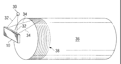
Figure 2a shows the modulator positioned to write onto or expose the drum.
The light could be positioned sc.~mewhere around position 30, and the light
would
l0 travel along path 32 to the modulator array 10. Typically, there are
optical
elements such as lenses or mirrors in this path. Since the geometry of the
path and
the combination of the elements have so many possible variations, they are not
shown.
As light from path 32 impinges upon the modulator, the selected cells on the
modulator direct their respective portions of the beam to the drum 36 along
path
34. The cells that are not selfacted to send light to the drum can be
configured to
either return light back to the source or to direct it away fxom the drum in
another
direction. The self;ction depcxnds on the confines of the optical system and
the
capabilities of the spatial light modulator.
2o Region 38 on drum 36 shows the area being exposed on the photosensitive
material on the face of the drum. Photosensitive, in the application, is meant
to
include any material that develops some kind of differentiation that can be
exploited for printing between areas exposed to radiation and areas not
exposed to
the radiation. The radiation is typically in the infrared to ultraviolet
range, due
Page 8
CA 02087625 2004-09-17
to the, availability of sources and optics, but is not assumed to be limited
to that
range. The photosensitive media could be intended for use as a negative for a
printing process, such as in printing negatives for printed circuit boards,
(PCBs), an
offset printing plate, a film or paper positive (a negative that has been
color or
contrast reversed), or other such items. Additionally, this media could be the
finished photographic product. For example, instead of making a negative to
pattern the PCB, the board itself could be patterned directly. Additionally,
other
items could be printed or exposed directly, such as film or paper positives.
Figure 2b shows what the data would possibly look like on the face of the
modulator 10 as if seen from the drum. The region 1 l, that is not hatched is
the
area being used to balance out the illumination profile.
In order to further overcome the limitation of rewriting the device every
cycle, an adaptation of the video chip is shown in Figure 3. A bank of shift
registers 40a-40b are now at the top of the modulator 10. This is used to load
the
data into the columns of addressing circuitry. This can be used to speed up
the
write time of the device during the OFF part of the cycle. Instead of
resetting the
device and then loading all of the data lines into the device from off chip,
switches
42a-42b are activated and the data currently in row 1 12 can be written up
into shift
register 40, the switches 42a-42b are then returned to the position shown and
the
data written down into row 2 14. Switches 44a-44b are closed as shown in this
figure for writing. Each set of switches, such as 42a and 44b, are tied
together
Page 9
CA 02087625 2003-05-15
such that when 42a is open 44b is closed and when 42a is closed 44b is open.
This
configuration of the device eliminates a vast amount of off chip processing,
and
limits the off chip accesses to one row of data per line time. This speed-up
will
decrease the OFF interval in the timing diagram of Figure 1b and also decrease
the
brightness loss discussed previously.
The final problem addressed by this invention is that of bandwidth. In the
method discussed in U.S. Patent No. 5,049,091, the output of the processor
driving
the device would typically be ~OMhz or 500 x 10a. In order to write 1000
columns,
the entire device, at that data rate, the load time must be 1000/50 x 106,
which
equals 20 x 10-6, (20 .seconds)" Most binary (ON/OFF) spatial light modulators
cannot be fully refreshed in 20 pseconds.
However, if the number of pixels to be written increased, by lining chips up
together, (if the chip size was fixed), this could be reduced. Two 768 x 576
pixel
chips together would mean that the processor would write 1536 columns per line
so the line time would be 1536/50 x 106, or 30 pseconds, which is more
reasonable,
as the device refresh rate for modulators such as the DMD is approximately
p,seconds ( .5 p.seconds per line, loading 50 lines from the top, and
50 lines from the bottom, simultaneously, equals 25 pseconds). Three chips
used
in tandem would give even more flexibility within a given time frame.
20 Three chips of 768 pixels wide have a time of 2304/50 x 106, or 46 seconds.
At this point the present embodiment of the invention is limited in speed
not by the modulator, but by the output of the data, at
Page 10
CA 02087625 2004-09-17
50 M~iz. Additionally, if the array size is not fixed, and one could use a
chip that
was larger, such as 1920 x 1080 pixels, the writing time would obviously be
lengthened even more.
In short, a standard modulator with standard addressing can emulate or
surpass the performance of a system using a customized device, using 100 of
its 576
available rows. The standard modulator also give two further advantages. The
first
is system flexibility. With an array such as 768 x 576, instead of 1000 x 100,
there
are more rows to be used: The use of multiple devices allows the designers to
consider a trade off not previously available. For example, using the 46
usecond
0 margin discussed above, another 25 lines on top and bottom could be loaded.
This
would take 37.5 useconds, and add a total of 50 lines of data. They can use a
lamp
that does not have to be as bright as the current source, making it cheaper.
The
trade offis that the third device may cost more. Another consideration not
previously
available is resolution control. The extra rows on the modulator can be used
to
5 increase the resolution, allowing the equalization of the illumination
profile to be
more exact.
The second advantage not available in the customized-device system, is the use
of already-established addressing schemes. An example of some of these schemes
can
be found in U.S. Patent No. 5,278,652. Further, using the standardized
0 modulator, which has data inputs on both the top and bottom, an addressing
scheme
could be used that accesses both the top and bottom of the modulator, as
previously
mentioned.
Page 11
CA 02087625 2003-05-15
An example of chips used in concert is shown in Figure 4. The light
impinges upon the modulators 10a, l Ob, 10c, simultaneously. The light from
the
selected cells of the devices well impinge upon the drum 36. The devices would
most likely have to be aligned to eliminate the gaps between the right-most
column
of cells 48a, on device 10a, and the left-most column 46b, of device :lOb, and
between 48b and 46c;. One of t:he many advantages of this is that the arm
holding
the devices (not shown) woulc:l only have to be repositioned one third as many
times as previously required. 'hhis again lowers the amount of time used
overall.
'lChis could also be repeated for as many devices from which the optics can
effectively receive light. It is possible that an entire line of devices could
be set
together so that thc~ entire drum is exposed in one positioning of the arm,
eliminating any possible errors from incorrect positioning during the steps
across
the drum.
Thus, although there has been described to this point particular embodiments
of a method of printing using spatial light modulators with standard
addressing
circuitry, it is not intended that such specific references be considered as
Limitations upon the scope of this invention except in-so-far as set forth in
the
following claims.
Page 12