Note: Descriptions are shown in the official language in which they were submitted.
~l~rlal~~
i
COMMUNICATION SYSTEM AND METhIOD
BACKGROUND OF THE INVENTION
(1) FIELD OF THE INVENTION
The present invention relates to a communication
system and method for use in an industrial process
that enables signals to be transmitted to and
received from a controlled device and specifically
relates to a novel electro-pneumatic instrument that
receives both power and analog control signals on a
single pair of conductors while also communicating
digitally with the control system in a bidirectional
manner on the same single pair of conductors.
210'519
2
(2) DESCRIPTION OF RELATED ART
It is well known in industrial systems to use
transducers, also called I-to-P transducers and
positionera to respond to a control signal and change
the position of a valve or the like in response to
the control signal. These devices are those that are
both powered and receive their control signals as a
4-20 milliamp DC signal via a single pair of
conductors and that can operate on any such level of
current with a maximum voltage that is usually no
more than 12 volts DC at the terminals of the
device. The combined current and voltage limitations
are often driven by the need to use these instruments
in hazardous area where only intrinsically safe
energy levels may be present.
Many devices that meet these requirements exist '
but most are analog in nature and do not possess the
ability to receive digital information from other
devices and to transmit digital information to such
other devices. One example of the prior art, the
go~emounnt 3311 device, superimposes a variable
=requency on the conductor pair as a means of
communicating information unidirectionally. Another
example of the prior art is disclosed in U.S. Patent
No. 4,633,217 which digitally transmits information.
Hoth ~»unt 3311 device and the device disclosed in
U.S.~Patent No. 4,633,217 are capable of digital
transmission only. They do not receive any signals
other than the 4-20 milliamp analog signal.
There are other transducer or positioner devices
that commLsicate bidirectionally but not via the same
210~~1~
3
single pair of conductors that carry 4-20 milliamp
power and the control signal. There are also many
process transmitters that have the primary function
of sensing process conditions rather than controlling
functions. These devices control the 4-20 milliamp
current rather than receiving it and many do
communicate digitally via the same conductor pair.
However, none of the controlled devices in the prior
art utilizes a single pair of conductors to receive
power and a 4-20 milliamp current control signal
while also transmitting digital information to and
receiving digital information from the control system.
It is important to note that control signal
transmitters control the loop current in the single
pair of conductors as a normal part of their
operation. Controlling the loop current independent
of the DC tern~inal voltage of the device is
equivalent to having a high DC impedance. Such a
device inherently allows modulation of the loop
voltage and can easily be paralleled with a like
device without fundamental changes in its interface
circuitry. However, communicating With these
controlled devices with another device such a process
control system requires a novel impedance
characteristic not present in transmitters. Also,
paralleling of multiple controlled devices when
communicating with a process control system requires
that the impedance be able to be changed or switched
to one similar to that of the transmitters.
In order for a transducer or positioner to have a
sufficiently low maximum DC terminal voltage at 20
milliamps loop current and have enough power
4
available to run a microprocessor circuit at 4
milliamps, it must have a low or negative impedance
at low frequencies. In order for such a device to
communicate digitally in both directions with one or
more other devices, it needs to have a relatively
high impedance at the communication frequencies. In
order for the communication signal, which carries
multiple frequency components, not to be distorted
substantially, the instrument s impedance must be
very high or essentially flat over the communication
frequency band.
Voltage headroom is a significant technical
obstacle when designing digital devices to operate
under the voltage and current restrictions stated
previously and still communicate digitally over the
same single pair of conductors. The microprocessors
have typically required 5-volt power at several
milliamps. The power requirements of other circuitry
can also be significant, particularly in the case of
transducers and positioners where an electro-
pneumatic output must be driven to perform the basic
instrument function.
Although the total current required in the device
usually exceeds 4 milliamp, the device itself needs
to operate on ~-milliamp loop current and thus it is
necessary to provide an efficient step-down power
conversion in the power supply circuitry of such
devices. Step-down conversion can be implemented in
three basic ways. First, by linear series
regulation; second, by inductor switching; or, third,
by capacitor switching. Series regulation is simple
and inexpensive but is very inefficient. Analog
21~'~51~
transducers can implement this type of regulation
because of a mush lower overall power requirement.
Inductor switching is quite common and versatile in
that it can be used to convert virtually any voltage
5 to any other voltage. This type of conversion
generates magnetic and electrical switching noise
that may be undesirable and generally cannot achieve
efficiencies greater than about 85 percent.
Capacitor switching can be greater than 90 percent
efficient and relatively quiet, but has the
restriction of converting voltages in integer steps.
As an example, the prior art 7660 switched capacitor
voltage converter can be used only to invert, double
or halve the input voltage.
The 5-volt logic of prior art could not employ
switched capacitor voltage conversion because the
requirement for 10-volt input to the converter could
not be met and still leave enough voltage headroom
for impedance control and modulation transmission
2o without exceeding a 12 VDC terminal voltage
requirement.
210751
.. 6
SUD~ARY OF THR INVENTION
The present invention maintains the application
advantages of the common 4-to-20 milliamp controlled
transducer or positioner with the use of a single
pair of conductors that supplies the power to the
transducer or positioner while also allowing digital
communication bidirectionally via the same single
pair of conductors.
The transducer or positioner can be sent a
multiplicity of digital instructions to change its
operating parameters where noncommunicating devices
would need to be physically removed, recalibrated or
locally manipulated in some manner to achieve the
change in operating parameters.
Further, the transducer or positioner can
communicate a multiplicity of information facts about
itself and its environment to other devices connected
to the same single pair of conductors thereby
improving the integrity of the control loop and
fulfilling the function of several instruments.
By utilizing the same single pair of conductors,
the instrument of,the present invention can be used
as a replacement for analog instruments without the
need to install additional conductors. The
instrument can be used in intrinsically safe
installations where higher powered devices cannot.
Further, digital signals can be used to comanunicate
with the circuit on a remote basis with the same pair
of conductors that power the device.
Thus, it is a feature of the present invention to
provide a novel instrument that is both powered and
2 .~ 0'~ ~u ~
controlled with a 4-20 milliamp control signal over a
single pair of conductors while digitally
communicating bidirectionally with other devices,
such as process control systems or other
communication terminals, via the same pair of
conductors.
It is also a feature of the present invention to
provide a novel instrument that has a low impedance
for the 4-milliamp DC control signals and relatively
nigh impedance for bidirectional digital
communication with one or more devices at the
communication frequencies.
It is still another feature of the present
invention to provide an auxiliary current sensor as a
part of the instrument that can sense an auxiliary
current controlled by a transmitter sensing pressure,
temperature, flow or some other variable and
transmitted on a second pair of conductors to the
communication instrument. One use of this auxiliary
signal is to sense a process feedback signal that is
compared with a commanded setpoint signal in a
process control algorithm and the resulting output
used as a setpoint to a servo-algorithm whose output
is used to control the electro-pneumatic device
function such as changing pressure or position. This
is accomplished while allowing the receiving or
transmitting of digital communication from a control
system or other communications tezzninal over a first
pair of conductors simultaneously with the power for
the device over the firsf pair of conductors.
Thus, the present invention provides a system for
communicating between a control system or
210'519
8
communication terminal and a remote electro-pneumatic
device or instrument that controls an actuator to
cause it to perform a task, the system comprising a
single pair of first and second conductors coupled
between the control system and the remote device for
carrying variable analog DC control signals to the
remote device to cause the remote device to perform a
selective task with the actuator, and enabling
bidirectional digitally encoded communication signals
concerning supplemental data to be transmitted
between the instrument input terminals and the
control system or other communication terminal over
the same single pair of first and second conductors.
~'he invention also relates to an instrument
capable of communicating with a control system or
other communication terminal through only two
conductors from a remote location with digital and DC
control signals and able to drive an actuator, the
instrument comprising first arid second input
terminals for receiving 4-20 milliamp variable DC
analog control signals on the two input terminals,
circuit means for receiving the DC input control
signals and generating actuator drive signals that
are coupled to the actuator as a function of the
input DC control signals, a circuitry for receiving
actuatoz condition signals from the actuator,
converting them to digital signals and coupling the
digital signals to the first and second terminals for
transmission to the remote control system or terminal
on the single pair of conductors and further
receiving digital command signals from the remote
control system or terminal through the same two
conductors and generating command signals to the
actuator.
9
The invention also relates to a voltage regulator
comprising a substantially constant voltage node
having a voltage, VN, on a first conductor with
respect to a second conductor, an operational
amplifier having first and second inputs and an
output, a series coupled resistor and zener diode
coupled across the first and second conductors to
provide a reference voltage to the first input of the
operational amplifier, first and second series
connected resistors, Rl and R2, connected across
the single pair of first and second conductors and
coupling the voltage across the second resistor,
R2, to the second input of the operational
amplifier to provide a voltage that varies with the
voltage at the substantially constant voltage node, a
transistor having a base,- emitter and collector with
the emitter and collector coupled across the single
pair of first and second conductors, and the output
of the operational amplifier being coupled to the
base of the transistor such that the voltage at the
substantially constant voltage node is regulated
according to the equation
VN = VR x CZ+(R~/R2)l
The invention further relates to a switched
capacitor voltage converter for receiving a fixed
regulated DC voltage, VREG and providing an output
voltage VREG/2 and -VREG/2 for providing power to
the circuit elements.
The invention also relates to a circuit that is
coupled to a single pair of first and second
~~o~~~~
0
conductors fox controlling the impedance of the
circuit presented to the single pair of conductors,
the circuit, the circuit comprising a variable
impedance element coupled in series with the first
input conductor and impedance control means coupled
to the variable impedance element far causing the
element to present a first acceptable impedance to
the single pair of conductors in response to a first
signal and to present a second substantially higher
impedance to the single pair of conductors in
response to a second signal.
11
BRIEF DESCRIPTION OF THE DRAWINGS
These and other objects of the present invention
will be more clearly understood when taken in
conjunction with the following DETAILED DESCRIPTION
OF THE DRAWINGS in which:
FIG. 1 is a front view of a diaphragm
actuated control valve that can be controlled by the
present invention;
FIG. 2 is a side view of the pneumatic
actuator portion of the control valve of FIG. 1;
FTG. 3 is a schematic drawing of the control
of the pneumatic actuator of FTGS. 1 and 2;
FIG. 4A is a diagrammatic representation of
a prior art control system operating a positioning
device such as the control valve of FIG. 1;
FIG. 4B is a diagrammatic representation of
the control system of the present invention that
utilizes both DC current and digital data in a
circuit to control a valve positioner such as that
disclosed in FIG. 1;
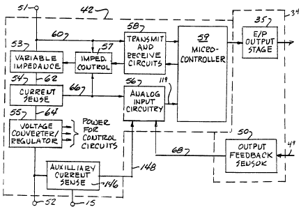
FIG. 5 is a block diagram of the circuit of
the present invention for receiving control signals
on a single two-conductor input, providing output
control signals to an electro-pneumatic driver for
the poeitioner or transducer and receiving feedback
signals for the positioner or transducer;
FIG. 6 is a detailed diagram of a portion of
the circuit of FIG. 5;
FzG. 7 is a block diagram of the present
invention including an auxiliary analog input signal
0 from a second pair of conductors for input of a
process variable such as pressure, temperature, flow
and the like;
210'~~10
12
FIG. 8 is a simplified schematic diagram of
a system using an auxiliary current sensor to receive
the auxiliary analog input control signal of FIG. 7;
FIG. 9 is a block diagram of the system
S illustrating the instrument control functions with
the addition of the auxiliary current sensor circuit;
FIG. 10 is a block diagram of the present
invention further including a switched capacitor
voltage converter to provide power for the control
circuits; and
FIG. 11 is a detailed schematic circuit
diagram of the switched capacitor voltage converter
and shunt regulator.
210' 519
13
D$TAILBD D$SCRIPTION OF T88 DRANINf3S
The present invention is basically used for
remote control of an actuator device over a single
pair of conductors from a remote distance. The
invention can be either a positioner or a
transducer. A positioner is defined as a device
which takes a primary electrical signal and
translates it into a position or movement. The term
"transducer", in the industrial system to which this
invention relates, generally refers to a device that
takes a primary signal and changes it to a quantity
such as a pressure. Since the present invention
pertains to both a positioner and a transducer,
Applicant will use throughout the specification the
team "transducer", for simplicity, but it is to be
understood that the term "transducer" is used herein
as both a positioner and a transducer as defined
herein.
A plan view of a diaphragm actuated control valve
10 is shown in FIG. 1. The actuator 16 includes a
rod 14 that controls the valve unit 12. Pressure
within actuator 16 forces the rod 14 to move against
a spring (illustrated schematically in FIG. 3) to
position the valve in valve unit 12 in a well-known
manner. A source of fluid pressure 18 is coupled
through position device 20 to actuator 16 to move the
rod or stem 14. A position device 20 is mounted on
the body of the actuator 10 and receives a feedback
linkage 19, shown in FIG. 2, that is coupled to the
rod or stem 14 to generate a feedback signal to
indicate the response of the unit to an applied
2~0'~53.9
14
signal. As can be seen in FIG. 3, a 4-20 milliamp DC
signal is applied from a remote control system
through a single pair of conductors to the position
device 20. The signal is converted by means in the
position device 20 to allow more or leas fluid
pressure from a supply 18 to be coupled through
control line 24 to the actuator 16 to move rod or
stem 14. The feedback is then coupled by feedback
linkage 19 to the position device to indicate
movement of the valve to the appropriate position
commanded.
FIG. 4A illustrates a prior art system for
operating such a valve. The transducer 34 receives
command signals from a remote controller 32 through a
single pair of conductors 33. The control signal is
typically a 4-20 milliamp DC signal having a voltage
sufficient to supply a minimum required voltage at
the input to the terminals of transducer 34. When
controller 32 sends the variable DC signal to the
transducer 34, it operates the transducer and
subsequently the valve to move an amount commanded by
the 4-20 milliamp DC signal. A sensor 36 generates
feedback signals on the single pair of conductors 37
which are coupled back to the control system 32.
Thus the controller infers from process feedback when
the tr2:nsducer 34 has responded properly to the
command signals. The signals used herein and
developed herein are analog in nature and do not
allow any other communication by the transducer 34 to
the control system 32. It would be advantageous to
be able to ask the transducer for additional
15
operational data on pressure, position, temperature,
ox some other related variable. For instance, it may
be desirable to know the temperature of the
transducer. It may also be desirable to know the
fluid output pressure at the transducer. It may also
be desirable to know the flow rate through the valve
that has been controlled or the pressure in the fluid
line which is controlled by the valve. Obviously,
other process related variables are important and
would be important to know during the operation of
the system.
The present invention provides such a device with
the use of a circuit illustrated in FIG. 4B. This
circuit is essentially identical in the overall
configuration to the circuit of FIG. 4A except that a
communication circuit 42 has been added to the
transducer 34 to provide an instrument 43 that
enables digital command signals to be received from
the control system 32 on the single pair of lines 35
and to return digital signals representing
operational data to the control system 32 on the same
pair of conductors 35. Thus the novelty of the
circuit in FIG. 4B is to maintain the application
advantages of the common 4-20 milliamp DC controlled
transducer while also allowing digital communication
bidirec~ionally with the control system and the
instrument 43 through the same single pair of
conductors 35. Thus with this circuit, the
instrument 43 can be sent a multiplicity of digital
instructions to report its operating parameters or to
change its calibration and/or configuration where
noncommunicating devices would need to be physically
removed, recalibrated or locally manipulated in some
210~~i~.9
16
manner to achieve the result. The circuit in FIG. 4B
can be used to communicate a multiplicity of
information data about the transducer itself and its
environment to other devices connected to the same
conductor pair thereby improving the integrity of the
control loop and fulfilling the function of several
instruments. Therefore, by replacing the analog
transducer 34 in FIG. 4A with the instrument 43 in
FIG. 4B, the instrument 43 can be used as a
replacement for prior art analog instruments without
the need to install additional conductors, can be
used in installations where separately powered
devices cannot, and can receive remotely generated
communications using the same pair of conductors that
power it. Thus, the circuit in FIG. 4B provides a
system for communicating between a control system and
the input tezininals of a remote instrument 43 that
controls an actuator to cause it to perform a task.
'The system comprises a single pair 33 of first and
second conductors coupled between the control system
32 and the remote instrument 43 for carrying variable
analog DC control signals to the instrument 43 to
cause the instrument 43 to perform selective tasks
with the actuator device. The instrument 43 is
2~ coupled to the single pair of first and second
conductors 33 for receiving the variable analog DC
control signals and simultaneously enabling
bidirectional digitally encoded communication signals
concerning supplemental transducer data to be
transmitted between the instrument input terminals
and the control system over the same single pair of
first and second conductors.
2~.p7~1~
17
FIG. 5 is a block diagram of the novel
communicating instrument 43 coupled to the actuator
35. Aa can be seen in FIG. 5, the communicating
instrument 43 includes the elements represented by
the block diagrams within the dashed lines 34 and
42. The two input terminals 51 and 52 represent the
instrument terminals that receive the 4-20 milliamp
DC signals on the single conductor pair 35. In order
for the transducer 34 to have a terminal voltage at
or below an acceptable DC level at 20 milliamps loop
current and to have enough power available to run a
microprocessor circuit at 4 milliamps, it must have a
low or negative impedance at low frequencies. In
order for the transducer to communicate digitally in
both directions with one or more devices, the
instrument 42 must have a relatively high impedance
at the digital communication frequencies. Further,
in order for the digital communication signal, which
carries multiple frequency components, not to be
distorted substantially, the impedance of the
communication instrument 42 must be very high or
essentially flat over the communication frequency
band.
To meet these objectives, the invention comprises
a variable impedance line interface circuit that
maintains a low impedance at frequencies below 25 Hz
to accommodate 4-20 milliamp analog signal variations
without substantial terminal voltage fluctuation
while also maintaining a substantially higher and
relatively constant impedance across the 500-5000 Hz
frequency band used for the digital communications.
210'~51~
18
In FIG, 5, terminals 51 and 52 comprise the main
terminals of the communication instrument 42 to which
the 4-20 milliamp loop formed by the single pair of
conductors 33 is connected. Variable impedance
element 53 regulates the total current drawn by the
instrument 42 to maintain the required impedance.
The characteristics of the impedance contral circuit
57, which monitors the voltage of terminals 51 and 52
and the current sensing element 54, determine the
apparent device impedance. Since the terminal
impedance at communication frequencies is
substantial, communication signals from other devices
can be extracted by the transceiver circuits 58
simply by monitoring and filtering the voltage on
terminals 51 and 52 through line 60. The transceiver
circuits 58 can readily transmit information by
modulating the impedance control device 57 which in
turn controls the variable impedance element 53 to
affect the terminal voltage and possibly the loop
current.
The current sensing element 54 is used
additionally by analog input circuitry 56 to monitor
the loop current for extraction of the DC analog
signal value for use as a control parameter. .As an
additional function of the instrument, the analog
input circuitry 56 can monitor one or more sensors
such as output feedback and other physical
properties. To receive and operate on digital
communications, and to carry out the primary function
of the circuit 42, the invention incorporates a
microprocessor or microcontroller circuit 59
interfaced to the analog circuitry 56 and the
2~0~~1~
19
transceiver circuits 58 as well as to an
electro-pneumatic output driver circuit 34. Many
prior art microcontrollers, such as microcontroller
59, transceivers such as transceiver 58 and analog
input circuits 56 are well known in the art and will
not be described in detail herein. Further, the
electro-pneumatic driver circuit 34 for a transducer
and its feedback sensor 50 are also well known in the
art as disclosed in relation to FIG. 1.
The variable impedance device 53 maintains the
low impedance at frequencies below 25 Hz to
accommodate the 4-20 milliamp DC analog signal
variation without substantial terminal voltage
fluctuation and also maintains a substantially higher
and relatively constant impedance across the 500-5000
Hz frequency band used for digital communications.
The impedance control device 57 causes the variable
impedance 53 to provide the impedance characteristic
needed. The current sense element 54 is used by the
analog input circuitry 56 to monitor the loop current
for extraction of the analog signal value for use as
a control parameter. As will be seen hereafter, as
an additional function of the instrument, the analog
input circuitry 56 can monitor one or more other
sensors such as output feedback signals or signals
representing other physical properties.
The voltage converter/regulator 55 provides the
power for the control circuits as indicated.
Thus the invention disclosed in FIG. 5 includes a
transceiver 58 coupled to the impedance control means
57 and to the single pair of conductor terniinals 51
and 52 for receiving the digital communication
210~~1~
signals from the controller on the single pair of
conductors at substantially higher frequencies than
the DC signals. The transceiver and the
microcontroller 59 can decode, filter, buffer,
5 demodulate, accumulate and/or convert the digital
information an the single pair of conductors from
serial to parallel as needed. The transceiver 58
transmits digital information to the control system
32 by processing the digital signals to provide
ZO parallel-to-serial conversion, modulation and/or wave
shaping as needed and coupling the digital signals to
the impedance eontrol means 57. The impedance
control means 57 controls the impedance of variable
impedance element 53 to affect the terminal voltage
15 and possibly the loop current of the single pair of
conductors coupled to terminals 51 and 52 for both
the variable DC and the second substantially higher
band of frequencies. Further, current sense element
54 is coupled in series with one of the single pair
20 of conductors and has an input and an output with an
analog circuit 56 coupled to the output of the
current sense element 54 to extract the DC analog
control signal from the single pair of conductors to
provide the desired output signal to the
microcontroller 59. Electrical conductors 68 couple
transducer and/or actuator feedback signals to the
analog input circuitry 56 for monitoring physical
properties of the transducer and/or actuator such as
pressure or.poaition. The microcontroller circuit 59
is coupled to the analog input circuit 56 and the
transceiver 58 to receive the DC analog control
signals on the single pair of conductors and to
210'~51~ 'v;
21
operate on the digital communication signals received
on the single pair of conductors at a second band of
substantially higher frequencies and transmits
digital communication signals on the single pair of
S conductors representing the physical properties of
the transducer and/or the actuator and other
information, e.g. serial number.
FIG. 6 illustrates a more detailed circuit of an
embodiment of the present invention. The 4-20
milliamp DC variable analog signal and the digital
signals from the controller 32 as illustrated in
FIG. 48 are coupled on the single pair of conductors
33 to input terminals 51 and 52. The signal on line
60 is coupled to a semiconductor element such as an
N-channel FET 53 having input, output and control
terminals formed with its drain, source and gate
terminals, respectively. The input and output
tezminals are in series with the conductor coupled to
terminal 51. FET 53 is the variable impedance
element that will provide the desired device
impedance characteristic when appropriately
controlled. Qne skilled in the art will recognize
that other types of transistors or semiconductor'
combinations can be substituted for this element.
pperational amplifier 80 is an impedance control
device whose output is coupled on line 78 to the
control terminal or gate of FET 53 to provide the
desired impedance characteristic as will be discussed
hereafter.
The output of the N-channel FET 53 is coupled on
line 84 to a resistor 54 which is the current sense
element illustrated in FIG. 5. This current sense
210' ~ ~. 0
22
element 54 provides the current sensing function for
impedance control as well as for the sensing of the
4-20 milliamp DC analog signal. Alternatively,
separate current sense elements can be used to
provide signals for these two functions. The output
of the current sensing element 54 at node 98 is
coupled to a shunt regulator 55 coupled between node
98 and common input line 52. Shunt regulator 55 is
the internal power supply voltage regulator. Tt
provides a substantially constant voltage at node 98
with respect to line or node 52 over the full range
of loop current and with a varying current load from
other connected circuitry. Any excess current
flowing in the loop, not required for powering the
control circuitry, is shunted by this element as will
be seen hereafter. The function of this device could
also be provided by other common circuits such as a
zener diode, a commonly available shunt regulator
integrated circuit, a transistor circuit or an
operational amplifier circuit.
The impedance control circuit comprises
components as follows: resistors 70 and 72,
capacitors 74, operational amplifier 80, capacitor
82, resistors 86 and 87, capacitor 100, resistors 102
and 104 and single-pole double-throw switches 106 and
108. To understand this circuit, the DC or
steady-state function is analyzed with the switches
106 and 108 in the position indicated by the solid
line. Eliminating the capacitors from the circuit
for DC analysis, it can be seen that amplifier 80
will manipulate the gate voltage of the N-channel FET
53 to maintain the following relationship:
34 V51-V52 ~ IV98 V52] x IR104/(R102+R104)) x Il+(R70/R72)1
2J.U'~<~J.~
23
This analysis assumes the values of R70, R72'
8102 and 8104 are chosen to allow sufficient
voltage drop across N-channel FET 53 so as to prevent
its saturation.
The analysis also shows that the DC average
terminal voltage of the device will be constant which
equates to a very low DC impedance, the advantages of
which were discussed earlier. It can be seen that
non-zero DC impedance will result if additional
impedance elements are added in series with the
circuit shown or if limited gain control elements are
used.
The addition of capacitor 82 to the circuit
causes the impedance of the device to rise with
increased frequency because it couples the voltage
across the current sense resistor 54 into the
impedance control amplifier 80 in such a way so as to
oppose changes in the input signal or loop current.
This increase in device impedance at higher
frequencies is necessary to facilitate digital
communir:ation among multiple connected devices. The
addition of capacitor 100 coupled between the
substantially constant voltage caused by voltage
regulator 55 and the differential amplifier 80 on
line 90 and the addition of capacitor 74 between
input terminal 51, coupled to one of the single pair
of conductors, and the input to amplifier 80 on
conductor 90 causes the impedance to level off at a
relatively fixed value above a predetermined cut-off
frequency. This leveling of the impedance
characteristic is targeted for the digital
communication frequencies and is necessary to limit
210'~01~
24
communication signal distortion. As shown in FIG. 6,
two single-pole double-throw switches 106 and 108 are
used to change the impedance characteristic of the
circuit from a special characteristic with very low
DC impedance and relatively high communication
frequency impedance to a constant high impedance
regardless of frequency. These switches may be
electrical switches of a type well known in the art
that are manually preset but could be operated by
signals from the microprocessor 59 by signals such as
on line 179. This alternate impedance characteristic
is necessary to allow the instrument to be used in
parallel with several other loop powered devices
where the current drawn by each is limited and
relatively constant rather than being varied as an
analog signaling means.
Thus, the N-channel FET 53 forms the variable
impedance element and is coupled in aeries with the
first input conductor 51 with its gate coupled to the
differexitial amplifier 80 that receives its input
signals through switches 106 and 108 to form an
impedance control means coupled to the variable
impedance element 53 for causing the variable
impedance element to present a first acceptable
impedance to the single pair of conductors coupled to
terminals 51 and 52 in a first frequency range below
25 Hz and to present a second substantially higher
impedance to the single pair of conductors in a
second frequency range of 500-5000 Hz. A first
voltage divider network. comprising series connected
resistors 102 and 104 is connected across the
terminals 51 and 52 at node 98 that has the
210519
substantially constant regulated voltage. A first
voltage is generated on node 92 that represents a
predetermined portion of the regulated voltage at
node 98 and is coupled through switch 108 to the
5 negative input of the differential amplifier 80. A
second voltage divider comprised of aeries connected
resistors 70 and 72 is connected across the input
terminals 51 and 52 and generate a second voltage on
node or line 77 that represents a predetermined
10 portion of the input voltage at the drain terminal of
the N-channel FET 53. The second voltage on node or
line 77 is coupled through the second switch 106 to
the second or positive input of the differential
amplifier 80. Thus the ratio of the unregulated
15 input voltage and the regulated output voltage drives
differential amplifier 80 to produce an output on
line 78 to the gate of N-channel FET 53 to regulate
its impedance. A variation of the second voltage
with respect to the first voltage caused by a
20 variation of the voltage across the single pair of
conductars connected to terminals 51 and 52 and the
drain terminal of the N-channel FET 53 varies the
impedance of the N-channel FET to present a low
impedance to the single pair of input conductors 51
25 and 52. Thus the gate voltage of the N-channel FET
53 ie varied by the output voltage of differential
amplifier 80 to maintain the following relationship:
VIN = V1 x L1+(R70/R72)1
where:
VIN = the input signal voltage to the
circuit on the single pair of conductors connected to
terminals 51 and 52';
214~51~
26
V1 = the first voltage produced by VREG
and the first voltage divider network comprised of
series connected resistors 102 and 104 such that
Vl VREF x IR104~(R102+R104~1~ and
VREG ' the substantially constant voltage
at the output of the sense element 54 on node or line
98.
When the switches 106 and 108 are moved from
their first position as shown to the second position,
a high impedance is presented to the input terminals
51 and 52 by the circuit 42. In that case, a third
voltage divider, formed by series coupled resistors
86 and 87, extends from the input to the current
sensing element 54 on line or node 84 across the
conductors coupled to terminal 51 to the second
conductor input terminal 52 to generate a third
voltage. This voltage is coupled by switch 108, in
its second position, to the negative input of
differential amplifier 80 while switch 106, in its
second position, couples the first voltage on line or
node 92 from the series coupled resistors 102 and 104
to the positive input of the differential amplifier
80. The output of the differential amplifier 80 on
line 78 that is coupled to the gate of the N-channel
FET 53 now causes the N-channel FET 53 to change its
impedance from its first characteristic impedance to
a second substantially higher impedance. Thus, as
stated, the N-channel FET 53 with the voltage coupled
to its gate.from differential amplifier 80 and the
Circuits providing the input to the differential
amplifier 80 form and impedance transformation
circuit coupled across the single pair of first and
second input conductors coupled to terminals 51 and
210' ~ ~. ~
27
52 for changing the impedance of the circuit
presented to the single pair of conductors on
terminals 51 and 52.
The transceiver circuit 58 is old and well known
in the art and will not be described in detail.
However, it is necessary to filter, buffer,
demodulate, accumulate and/or convert the digital
information sent to it from other devices on the loop
from serial to parallel form as needed. The
transceiver circuit 8 may provide parallel-to-aerial
conversion, modulation, wave shaping (filtering)
and/or coupling into the impedance control circuit
for transmission purposes.
The analog input circuit 56 is also old and well
known in the art and can be used for a multiplicity
of useful functions. The one essential function in
this application is to monitor the loop current
developed across current sensor 54 as the primary
means for the control system to indicate the desired
output value to the pressure/position control
algorithm as will be shown hereafter. Other
functions for this analog input circuit 56 are
monitoring of the output feedback sensor 50 for
closed loop control, monitoring of electrical signals
from a multiplicity of other local sensors as will be
described hereafter or monitoring of the current or
voltage in one or more auxiliary circuits externally
connected via an additional conductor or conductors.
The microprocessor 59, which may be of any
well-known type in the art, is the primary control
element of the present invention. It may be
implemented with separate processing and memory
components or as a single chip microcontroller. It
21~~~1~
28
is required to decode and act upon digitally
communicated information on the single pair of
conductors 51 and 52 and to generate digital messages
containing a response or providing request data for
other devices. The microprocessor 59 may directly
implement a control algorithm that drives an
electro-pneumatic output stage 34 in response to
either analog or digital information or it may simply
provide a setpoint to an analog or pneumatic device
which controls the output. A multiplicity of other
functions may also be provided by the microprocessor
such as autocalibration, temperature compensation and
various control algorithms.
FIG. 7 discloses an alternate embodiment of the
present invention that can be used to receive 4-20
milliamp analog DC signals over an additional pair of
conductors with digital signals being transmitted by
and to the control room 32. In FIG. 7, transducers
such as a control valve 10 illustrated in FIG. 1 is
shown schematically with the actuator 16 driving a
stem or rod 14 to control the position of the valve
12. The change in position of valve 12 varies the
flow of fluid in line or pipe 138 and may change
other variables such as pressure and the like. As
described earlier, in relation to the control system
32, a digital control signal is transmitted on the
single pair of input lines 130 to terminals 51 and
52. The communication instrument 42 derives a
setpoint signal that is coupled to the
electro-pneumatic output stage 35. Stage 35 produces
a pressure signal on line 24 to actuator 16 that
moves rod 14 to position valve 12. The change in
210~5~J
29
pressure on line 24 causes a feedback to unit 50 or
the mechanical positioning of valve 12 causes a
mechanical feedback by device 19 to the feedback unit
50. It converts the pneumatic or mechanical feedback
into an electrical signal on line 68 to the
communications instrument 42. The microprocessor 59
in instrument 42 may then convert that signal to a
digital signal and transmit that signal back to the
control system on the single pair of lines 130 to
notify the control system of the new pressure or
valve position.
In addition, a two-conductor process transmitter
140 may be mechanically coupled to the line 138 to
detect a second process variable such as pressure,
temperature or the like by means of a transducer 137
coupled at 139 to process transmitter 140. It then
develops an analog signal on a single pair of lines
142 that is coupled back to terminals 51 and 15. The
current signal on terminals S1 and 15 is sensed by an
auxiliary current sensor 146 as shown in FIG. 8 and
is then coupled to the analog input circuitry 56 and
to the microprocessor 59 as will be discussed in more
detail in relation to FIGS. 8 and 9. The
microprocessor 59 then reads the setpoint from the
control room 32 and generates a servo-setpoint signal
that is coupled to the electro-pneumatic stage 34 for
control of. pressure or position depending upon
whether the device is a transducer or positioner.
Further details of the system in FIG. 7 are
illustrated in FIG. 8. The instrument of FIG. 8 uses
the two terminals 51 and 52 to connect to the single
pair of conductors 130 in FIG. 7 that go from the
instrument 42 back to the process control room.
210'~~1.~~
Power is delivered to the instrument through the two
conductors to terminals 51 and 52 in the form of a
minimum voltage and current and digital signals
create the digital setpoint as described previously.
5 The voltage converter/regulator 55 provides the
regulated power to the instrument circuits. The
digital signals at the two terminals 51 and 52 are
communicated from the control room and serves as the
initial control signal to the instrument. In the
10 circuit shown in FIG. 8, the microprocessor 59 is
used to provide the process control algorithm and a
servo-algorithm. As stated earlier, analog
servo-circuits external to the microcontroller 59
could also be used instead of a a digital
15 servo-algorithm. The output of the servo-algorithm
in the microcontroller 59 is used to control the
electro/pneumatic stage~35.
The output feedback sensor 50, which can be a
pressure sensor for a transducer or a position sensor
20 for a positioner, for example, generates a signal
that is coupled back to the analog input circuitry 56
and is used to generate an error signal in the
servo-algorithm in the microcontroller 59 and to
communicate the feedback value, independent of the
25 servo-algorithm. This device allows reception or
transmission of digital communication simultaneously
with the powering of the device over the two
conductors 51 and 52. The microcontroller 59,
connected to the transmit-and-receive circuit 58,
30 impedance control device 57 and the variable
impedance device 53 is used to produce a digitally
encoded current or voltage signal at terminals 51 and
~~.0'~ ~1.~
31
52 which has an average value of zero. To receive
digital data, the instrument uses transmit-and-
receive circuit 58 to receive the digitally encoded
current signals at terminals 51 and 52 and provides
the proper levels for input to the microcontroller 59
where it is decoded.
An auxiliary current sensor 146 is shown in FIG.
8 to sense the auxiliary variable input DC current
such as from the two-conductor process transmitter
140 on single pair of lines 142 in FIG. 7. This
current is used as the feedback to a process
algorithm contained within the microcontroller 59.
The process transmitter 140 in FIG. 7 may sense
pressure, temperature, flow or some other process
related variable and its single pair of conductors
142 is connected to the terminals 51 and 15. A
variable DC current controlled by the transmitter 140
and representing the process variable is sensed by
the auxiliary current sensor 146 in FIG. 8. The
operation of the microcontroller 59 on the current
sensed by sensor 146 is illustrated in more detail in
FIG. 9.
In the embodiment of FIG. 9, the output from the
auxiliary current sensor 146 is connected to the
analog input circuitry 56 as shown in FIG. 8 and then
to the microprocessor 59. Inside the microprocessor
59, this auxiliary signal becomes tre process
feedback signal to a process algorithm 116 where it
is compared to the digitally derived setpoint 114
coming from the digital decoding software 112.
Transmit and receive circuitry 110 in the circuit 42
(in Fig. 7? receives the digital signal on the single
2~U'~i~:l~
32
pair of conductors and couples it to software 112
which decodes it for the microcontroller 59 as
described previously to establish the setpoint 114.
The process algorithm 116 generates a new
servo-setpoint 122 for the servo-algorithm 124 by
comparing the set point 114 with the data from the
process transmitter 140. The servo-setpoint 122 is
then compared to the output signal from feedback
sensor 50 through the analog input circuitry 56.
Servo-algorithm 124 then generates a correction on
line 126 to the electro/pneumatic stage 34 for
control of the instrument output pressure where the
controlled device is a transducer or for a control of
a valve position where the control device is a
positioner. In an alternate embodiment, the process
or servo-algorithms 116 and 124 may be analog
circuits that the microcontroller 59 supervises in a
well-known manner. The system shown in FIGS. 8 and
9, as stated earlier, can also be used to transmit
and receive digital signals to and from the control
room 32 over terminals 51 and 52 as well as to
receive the analog signals from the current sensor
146 as described previously.
Thus, in FIGS. 7, 8 and 9, an auxiliary
transducer 137 is responsive to the operation of the
device 12, such as a control valve, for sensing an
auxiliary function such as temperature, pressure,
flow and the like process related variables and
generating a corresponding DC output electrical
signal. A process transmitter 140 is coupled to the
auxiliary transducer 139 for generating a DC output
current on a second single pair of third and fourth
210'~~~9
33
conductors 142 to first and third input terminals 51
and 15, respectively, of the communication instrument
42. An auxiliary current sensing device 146 has one
input coupled to the first tezzninal 51 and a second
input coupled to the third terminal 15 for generating
an output signal to the analog circuit 56 such that a
second output of the analog circuit 56 is coupled to
the microcontroller 59 as a feedback signal for
control purposes as described previously. Reviewing
FIG. 9, the first process algorithm 116 may be a
first comparator means in the microcontroller 59 for
comparing the input control signal 114 from the
single pair of input conductors on terminals 51 and
52 with the first output of the analog circuit 56
from the auxiliary current sensor 146 to establish a
first corrected control signal 122 and the
servo-algorithm 124 may be a second comparator means
in the microcontroller 59 for comparing the first
corrected control signal or servo-setpoint signal 122
with the second output of the analog circuit 56 from
the output feedback sensor 50 to establish a second
corrected servo-control signal 126 that is coupled to
and controls the electro/pneumatic output stage 35.
As can be seen in the circuit of FIG. 10, a
switched capacitor voltage converter 150 has been
added in parallel with the shunt regulator 55 to
provide power on terminals 152 for the control
circuits. The reminder of the circuit functions as
set forth previously. The details of the shunt
regulator 55 and the switch capacitor voltage
converter 150 are disclosed in FIG. 11.
Shunt regulator 55 is the internal power supply
voltage regulator. It provides a substantially
210'~~1J
34
constant voltage at node 172 with respect to a common
or ground node 174 (in FIG. 11) over the full range
of loop current with a varying current load from
other connected circuitry. Any excess current
flowing in the loop, not required for powering the
control circuitry, is simply shunted by the PNP
transistor 171 coupled across nodes 172 and 174. The
function of the shunt transistor 171 could be
provided by other circuits such as a zener diode, a
commonly available shunt regulator integrated
circuit, or a transistor circuit. In the circuit 55
as shown in FIG. 11, the input voltage, VIN, from
current sensor 54 on line 154 is coupled to node
172. Resistor 156 provides a reverse excitation
current to zener diode 158 which provides a voltage
reference, VREF at node 160 to line 162 and to the
noninverting input of operational amplifier 164. The
other input to the amplifier 164 is derived from the
series resistor combination 166 and 168 across nodes
172 and 174 such that any variation in the voltage at
172 causes a variation at node 170. Amplifier 164
drives the base of PNP transistor 171 to regulate the
voltage at node 172 according to the following
equation:
VIN ' VREF x (1+R166~R168)
where:
VIN is the regulated voltage at 172,
VREF is the reference voltage at 170, and
R166~R168 are fixed values chosen to
provide the desired regulated voltage, VREG'
given a chosen VREF'
2~0~5~~
Thus, the voltage regulator includes a current
shunting element 171 across the single pair of
conductors connected to terminals 51 and 52 for
shunting any excess current flowing in the two
5 conductors and not required for powering the
circuit. The current shunting element comprises a
substantially constant voltage node 172 having a
voltage, VIN, formed at the output of the current
sensor 54 with respect to terminal 52. An
10 operational amplifier 164 has first and second inputs
162 and 170, respectively, and an output to the base
of the shunting transistor 171. A circuit, including
resistor 156 and series coupled zener diode 158 has
node 160 coupled to the first input of the amplifier
15 164 on line 162. A series circuit formed of
resistors 166 and 168 is connected across the
terminals 51 and 52 and couples the voltage developed
across resistor 168 to the second input of the
operational amplifier 164 on line 170. Transistor
20 171 has its emitter and collector coupled across the
nodes 172 and 174, which is coupled across the single
pair of conductors to input terminals 51 and 52. The
output of the operational amplifier 164 is coupled to
the base of the transistor 171 such that the voltage
25 of the substantially constant voltage node 172 is
regulated according to the equation:
VIN m VREF x I1+(R1/R2)].
30 The output of the voltage regulator at nodes 172
and 174 is coupled to the switched capacitor voltage
~1.U'~~~.J
36
converter 150 for developing a voltage of
substantially VIN , VIN/2 and -VIN/2.
Capacitor 176 across the input lines 172 and 174 to
the switched capacitor voltage converter 150 filters
the regulated voltage on line 172 that is being
coupled to the switched capacitor voltage converter
150. Voltage converter 150 is comprised of a
switching device 178 which is well known in the art
and added circuitry that generates an additional
output.
Capacitors 176, 200 and 216 work in conjunction
with switching device 178 in a manner that is well
known and completely described in application notes
for commercially available switched capacitor voltage
converter integrated circuits to produce a voltage at
218 that is essentially one-half the input voltage at
220 with respect to 214.
Capacitors 202 and 212 and diodes 206 and 208
form a charge pump circuit which is also common and
well known in the art.
Node 198 as a normal function of the switched
capacitor voltage converter 178 is alternately
connected to nodes 218 and 214. This alternating
connection produces an AC signal that is readily
converted to a negative voltage by the charge pump
circuit. The output of the charge pump circuit as
shown will be negative with respect to node 214 and
will have a magnitude approximately equal to the
output of device 178 less the forward voltage drops
of diodes 206 and 208.
The novelty of voltage conversion circuit 150 is
the unique combination of the two known arts of a
~lUrl~l9
37
switched capacitor voltage converter and a charge
pump to produce a multiple output highly efficient
power supply which is uniquely applied to a
two-conductor 4-20 milliamp controlled device.
Thus it can be seen that the novel instrument 43
communicates with a control system from a remote
location with both digital and DC control signals for
driving an actuator. The instrument 42 comprises
first and second input terminals 51 arid 52 for
receiving both 4-20 milliamp variable DC analog
control signals and digital communication control
signals on the same two input terminals 51 and 52.
The instrument 43 includes a circuit 42 that converts
the input control signals to actuator drive
pressures. Pneumatic tubing couples the output
driving pressure to the actuator 16 as shown in
FIG. '3 in response to the input digital or DC control
signals. The instrument 43 receives instrument and
actuator condition signals, converts them to digital
signals and couples the digital signals to the first
and second terminals 51 and 52 for transmission to
the control room 32 on the single pair of conductors
and further receives digital communication signals
from the control room and generates pneumatic drive
signals to the actuator.
'Thus, there has been disclosed a novel remote
transducer instrument allowing communication between
a control system and the input tezminals of the
transducer over a single two-conductor pair with both
variable DC analog control signals and digital
communications such that it can not only control the
transducer device but also pass information to the
210'~~1.~
38
instrument related to diagnostics of the device or
the actuator 10 for transmission to the controller.
The diagnostics relate to operational data associated
with the device or the actuator 10 such as
temperature, pressure, position and the like. Thus,
a single pair of conductors allows both DC controlled
and digitally controlled diagnostic routines of the
transducer to be performed.
There has also been disclosed a novel impedance
transformation circuit used by the system and coupled
to the single pair of first and second input
conductors for changing the impedance presented to
the single pair of conductors to enable bath analog
signal communication at low impedances and digital
communication at high impedances as needed.
Further, there has been disclosed a novel circuit
for accepting an auxiliary analog input that can be
used as a feedback to a process control algorithm
contained within the communication system. The
auxiliary input DC current may be from a process
transmitter sensing pressure, temperature, flow or
some other process related variable. The novel
instrument can also be used to transmit to and
receive digital signals from the control room as well
as to receive the transmission of the analog signals
from the auxiliary process transmitter by using a
variable impedance and auxiliary current sensing
device.
Finally, there has been disclosed a novel. voltage
regulator and switched capacitor voltage converter
for accepting a level of DC current from 4-20
milliamps with a minimum DC voltage at its input
39
terminals and providing a regulated output voltage
that is stepped down far use with the communication,
monitoring and control circuitry.
Thus, the invention combines a low voltage
microprocessor with switched capacitor voltage
conversion and a novel variable impedance
characteristic to meet the requirements for the 4-20
DC milliamp operation and with bidirectional digital
communication on a single pair of conductors.
While the invention has been described in
connection with a preferred embodiment, it is not
intended to limit the scope of the invention to the
particular form set forth, but, on the contrary, it
is intended to cover such alternatives,
modifications, and equivalents as may be included
within the spirit and scope of the invention as
defined by the appended claims.