Note: Descriptions are shown in the official language in which they were submitted.
cat
CFO 9746 -~
1 - ~1~.~~:~
1 ELECTRON SOURCE, AND IMAGE-FORMING APPARATUS
AND METHOD OF DRIVING THE SAME
BACKGROUND OF THE INVENTION
Field of the Invention
This invention relates to an electron source
and an image-forming apparatus such as a display as
an instance of application~thereof, and more particu-
larly, it relates to an electron source provided with
a plurality of surface-conduction electron-emitting
devices, and an image-forming apparatus such as an
electronic display and a method of driving the same.
Related Background Art
Thermal cathods and cold cathode electron
sources are known two type of electron emitting
devices, of which the latter include field-emission
type (hereinafter referred to as FE type), metal/
insulation layer/rnetal type (hereinafter referred to
as MIM type) and surface-conduction electron
emitting devices.
Examples of FE type devices are proposed in
W. P. Dyke & W. W. Dolan, "Field emission", Advance
in Electron Physics, 8, 89 (1956), A. Spindt,
"PHYSICAL Properties of thin-film field emission
cathodes with molybdenum cones" J. Appl. Phys., 32,
646 (1961).
At MIM type device is disclosed in C. A. Mead,
- 2 - ~ ~ 10
~ ,~ ,4~ ..~
1 "The tunnel-emission amplifier, 3. Appl. Phys., 32,
646 (1961).
A surface-conduction type electron-emitting
device is proposed in M. T. Elinson, Radio Eng.
Electron Phys., 10 (1965).
A surface-conduction electron-emitting device
utili2es the phenomenon that electrons are emitted out
of a small thin film formed on a substrate when an
electric current is forced to flow in parallel with -
the film surface. While Elison proposes the use of
an Sn02 this film for a device of this type, the use
of an Au thin film is proposed in [G. Dittmer: '°Thin
Solid Films", 9, 317 (1971)] whereas the use of an
In203/Sn02 and that of a carbon thin film are
discussed respectively in [M. Hartwell and C. G.
Fonstad: "IEEE Trans. ED Conf.", 519 (1975)] and
[H. Araki et al.: "Vacuum"; Vol. 26, No. 1, p. 22
(1983) ] .
Fig. 43 of the accompanying drawings
schematically illustrates a surface-conduction
electron-emitting device groposed by M. Hartwell.
In Fig. 43, reference numerals 431 and 432
respectively denote an insulator substrate and an
H-shaped metal oxide film for electron-emission
formed thereon by sputtering. Reference numeral 433
denotes an electron-emitting region that becomes
operational when electrified in a process generally
W
- 3 - ~~ j ~r~? i
1 referred to as "forming", which will be described
hereinafter. The entire thin film including the
electron-emitting region is designated by numeral 434
in Fig. 43. For a device as illustrated in Fig. 43,
S L1 is between 0.5 and lmm and W is equal to 0.lmm.
An electron-emitting region 433 is produced in
a surface-conduction electron-emitting device
normally by electrifying a thin film 432 for
electron-emission on the device, a process generally
xeferred to as '°forming°'. More specifically, a DC
voltage or a slowly rising voltage that .rises, for
instance, at a rate of 1V/min. is applied to the
opposite ends of the thin film 432 for electron-
emission to locally destroy or deform or structurally
modify the thin film 432 for electron-emission to
produce fissures in a part of the.thin film, which
constitute an electrically highly resistive electron-
emitting region 433. Once the surface-conduction
electron-emitting device is processed for forming,
electrons will be emitted from those fissures and
their neighboring areas when a voltage is applied
to the thin film 434 including the electron-emitting
region 433 to cause an electric current to flow
through the device. ..
Known surface-conduction electron-emitting
devices are, however, accompanied by problems when
they are put to practical use. The applicant of the
s~~.~~~~~.
1 present patent application who has been engaged in the
technological field under consideration has already
proposed a number of improvements to the existing
technologies in order to solve some of the problems,
which will be described in greater detail hereinafter.
Surface-conduction electron-emitting devices
are, on the other hand, advantageous in that they can
be used in arrays in great numbers over a large area
because they are structurally simple and hence can be
manufactured at low cost in a simple way. In fact,
many studies have been made to exploit this advantage
and applications that have been proposed as a result
of such studies include charged beam sources and
electronic displays.
~" ;~.. ~ '' ~
1 light source needs to be additionally incorporated
into the display in order to illuminate the liquid
crystal panel because la.quid crystal does not emit
light by itself. An Emissive electronic display that
is free from this problem can be realized by using a
light source formed by arranging a large number of
surface-conduction electron-emitting devices in
combination with fluorescent bodies that are induced
to selectively shed visible light by electrons emitted
from the electron source. With such an arrangement,
Emissive display apparatus having a large display
screen and enhanced display capabilities can be
manufactured relatively easily at low cost. (See,
for example, the United States Patent No. 5066883 of
the applicant of the present patent application.)
Incidentally, Emissive display apparatus of
the above identified category comprising an electron
6
- 6 - ~ ~, a~.:~ ~1 a
1 1-283749 of the applicant of the present patent
application).
There are, however, a number of difficulties
that have to be overcome before such a display
S apparatus becomes commercially feasible. Some of the
difficulties include the problem of accurately
aligning individual surface-conduction electron-
emitting devices and corresponding individual grids
ahd that of securing a uniform distance between each
grid and the corresponding surface-conduction
electron emitting device, both of which are
1 electrodes 444 arranged perpendicularly to the
electron-emitting bodies 442 to form a lattice
therewith and a glass panel 443 provided with a number
of small hales 443' and disposed between the electron-
emitting bodies and the electrodes in such a manner
that the holes are located on the respective crossings
of the electron-emitting bodies and the electrodes.
Each of the holes 443' contains gas hermetically
sealed therein so that the display emit light by gas-
electric discharge only at the crossings of those
transversal current type electron-emitting bodies 442
that are currently discharging electrons and those
transparent electrodes 444 to which an accelerating
voltage E2 is currently being applied. While Japanese
Patent publication No. 43-31615 does not detailedly
describe the transversal current type electron-
emitting body, it may safely be presumed
that it is a surface-conduction electron-emitting
device because the materials (metal thin film, mesa
film) and the structural features of the neck 442'
described there exactly match their counterparts of
a surface-conduction electron-emitting device. Fore
the purpose of the present invention, the term
"surface-conduction electron-emitting device" is
used in the sense as defined in "The Thin Film
Handbook".
Now, some of the problems that have arisen
~v
_ 8 _
1 with electronic displays comprising known surface-
conduction electron-emitting devices will be discussed
below.
Three major. problems have been pointed out for
a display apparatus disclosed in the above cited
Japanese patent Publication No. 45-31615.
(1) While the display apparatus is designed
to operate for electric discharge as electrons emitted
from the transversal current type electron-emitting
bodies are accelerated and caused to collide with gas
molecules, the pixels of the apparatus can glow by
electric discharge with different levels of luminance
and the luminance of a same pixel can fluctuate when
the transversal current type electron-emitting bodies
are energized 'to a same intensity. One of the
possible reasons for this may be that the intensity
of electric discharge of such an apparatus is
heavily dependent on the state of the gas in the
apparatus and not satisfactorily controllable, while
another may be that the output level of a transversal
current type electron-emitting body cannot necessarily
be stabilized if 'the gas pressure is somewhere around
lSmmHg as described in the Examples section of the
cited patent document.
Thus, the above described display apparatus is
not able to provide any multiple-tone display and
~~.~.~~~~?1.
1 therefore can offer only a limited scope of use.
(2) While the display apparatus can change
the colox fox display by using a different type of
gas, the use of various gases does not necessarily
extend the scope of color display because the wave-
length of visible light generated by electric dis-
charge does not cover a wide range. Additionally,
the optimum gas pressure used for the emission of
light by electric discharge varies as a function of
the type of gas involved.
Thus, in order to achieve a color display by
using a single panel, different gases must be sealed
in the holes with varied gas pressures depending on
the locations of the holes, making the manufacture
of such an apparatus extremely difficult: If, for
example, three laminated panels are used for a display
apparatus to avoid this problem, it will become
unrealistically heavy and the manufacturing cost will
be prohibitive to produce such a heavy apparatus.
(3) Since the display apparatus comprises a
large number of components including the substrates
of the transversal current type~electron-emitting
bodies, the strip-shaped transparent electrodes and
the holes where gas is hermetically sealed, it is
structurally very complicated and hence only a very
small error margin is allowed for aligning the
components. Additionally, since the threshold
r
voltage used for the emission of light by electric
discharge is as high as 35(V] as described in the
cited document, each electric element used in the
panel drive circuit is required to show a high
withstand voltage.
Thus, such a display apparatus will require a
complicated process to follow before it is completed
as well as a prohibitive manufacturing cost.
It is mainly due to the above reasons that an
electronic display of the above described type has
not been able to find any practical applications in
the field of television receiving set and other
similar electronic apparatuses.
On the other hand, the image-forming
~.5 apparatuses proposed by the applicant of the present
patent application and comprising an electron source
formed by arranging a number of surface-conduction
electron-emitting devices and a same number of
fluorescent bodies juxtaposed therewith are not
without problems.
Firstly, in order to realize such an electron
source, it is indispensable to arrange grids along~a
direction (column-directed wiring) perpendicular
to the wires connecting the electron-emitting devices
2~ arranged in parallel (row-directed wiring) if the
devices are selectively made to emit electrons.
In this regard, no simple and easy process has been
- 11 -
1 developed for manufacturing an electron source with
which devices are selected for the emission of electrons
and the level of electron emission is controllable.
Secondly, in order for the fluorescent bodies
of such an image-forming apparatus arranged in
juxtaposition with the electron source to emit light
at selected locations with a controlled level of
luminance, a certain number of grids need indispensably
be provided as in the case of the electron source.
Again, no simple and easy process has been developed
for manufacturing an image-forming apparatus comprising
such fluorescent bodies, with which electron--emitting
devices can be selected with difficulty to cause them
emit light at a controlled level according to
incoming signals so that the fluorescent bodies may
be made to glow at selected locations with a controlled
level of luminance.
SUMMARY OF THE INVENTION
In view of the'above identified problems,
it is therefore an object of the invention to provide
a novel electron source comprising a large number of
surface-conduction electron-emitting devices adapted
to be selectively energized to emit electrons at
varied amounts under the control of input signals.
According to the invention, such an electron source
can be manufactured at low cost because of it simple
- 12 - ~~ 9.2~? ~_
1 configuration and used in combination with a fluo-
rescent material arranged vis-a-vis the electron
source to produce a high quality image-forming
apparatus capable of displaying images in color and
in a multitude of tones. It is another object of
the present invention to provide a method of
effectively driving such an electron source.
Still another object of the invention is to
pxovide an image-forming apparatus comprising such
an electron source and capable of displaying images
with good gradation as well as a method of effectively
driving the same.
A further object of the invention is to
provide an image--forming apparatus comprising such an
electron source and an image display screen provided
with pixels that are ingenuously so configured as to
be tree from crosstalks.
According to an aspect of the invention, the
above object are achieved by providing an ezectron
source adapted to emit electrons as a function of
input signals comprising a substrate, a matrix of
wires having m row wires and n column wires laid on
the substrate with an insulator layer interposed
therebetween and a plurality of surface-conduction
electron-emitting devices each having a pair of
electrodes and a thin film including an electron
emitting section and arranged between the electrodes,
1 the electron-emitting devices being so arranged as
to form a matrix with the electrodes connected to the
respective row and column wires, the electron source
further comprising selection means for selecting and
some of the plurality of surface-conduction electron-
emitting devices and applying modulation signals
thereto and modulation means for generating modulation
signals according to input signals and applying them
to the surface-conduction electron-emitting devices
selected by the selection means.
According to another aspect of the invention
the above objects are achieved by providing an image-
forming apparatus adapted to form images as a function
of input signals comprising an electron source and an
image-forming member, the electron source by turn
comprising a substrate, a matrix of wires having m
row wires and n column wires laid on the substrate
with an insulator layer interposed therebetween and
a plurality of surface-conduction electron-emitting
devices each having a pair of electrodes and a thin
film including an electron-emitting section and
arranged between the electrodes, the electron-
emitting devices being so axranged as to form a
matrix corresponding to that of pixels of the
apparatus with the electrodes connected to the
respective row and column wires, the image-forming
- 14 -
1 selecting and some of the plurality of surface-
conduction electron-emitting devices and applying
modulation signals thereto and modulation means for
generating modulation signals according to input
signals and applying them to the surface-conduction
electron-emitting devices selected by the selection
means.
BRIEF DESCRIPTION OF THE DRAWINGS
Figs. lA and 1B are schematic views illus-
trating the basic configuration of a plane type
surface-conduction electron-emitting device that can
be used for the purpose of the present invention.
Figs. 2A through 2C are schematic views
illustrating different steps of manufacturing a
surface-conduction electron-emitting device to be
used for the purpose of the invention.
Fig. 3 is a bloc7c diagram of a measuring
system for determining the performance of a surface-
conduction electron-emitting device to be used for
the purpose of the invention.
Fig. ~ is a graph showing a voltage waveform
to be used for forming a surface-conduction electron-
emitting device to be used for the purpose of the
invention.
Fig. 5 is a graph showing the relationship
between the voltage applied to a surface-conduction
'"1 ,
- 15 - ~~.~.~r~U_~
1 electron-emitting device to be used for the purpose
of the invention and the current that flows there-
through as well as the relationship between the
voltage and the emission current of the device.
Fig. 6 is a schematic perspective view of a
step type surface-conduction electron-emitting device
that can be used for the purpose of the invention.
Fig. 7 is a schematic plan view of an electron
source according to the invention.
Fig. 8 is a schematic perspective view of an
image-forming apparatus according to the invention.
Figs. 9A and 9B axe schematic views illus-
trating two types of fluorescent films that can be
used for the purpose of the invention.
Fig. l0 is a schematic circuit diagram
illustrating the method of driving fluorescent
materials for the purpose of the invention.
Fig. 11 is an exploded and enlarged per-
spective view of an electron-emitting device and a
face plate of an image-forming apparatus according
1 beam in an image-forming apparatus according to the
invention and comprising surface-conduction
electron-emitting devices.
Fig. 14 is a schematic plan view of a first
embodiment of electron source of the invention.
Fig. 15 is a schematic sectional view of the
first embodiment of Fig. 14.
Figs. 16A through 16D are schematic sectional
views of the first embodiment, showing it in different
manufacturing steps.
Figs. 17E through 17H are schematic sectional
views of the first embodiment, showing it in different
manufacturing steps following that of Figs. 16A to 16D.
Fig. 18 is a schematic plan view of a mask
that can be used for the first embodiment.
Fig. 19 is a graph similar to Fig. 5 but
showing the voltage-current relationships for a
specimen prepared for the purpose of comparison.
Fig. 20 is a schematic sectional view of a
second embodiment of electron source of the invention.
Figs. 21A through 21F are schematic sectional
views of the second.embodiment of Fig. 1'4, showing
it in different manufacturing steps.
Fig. 22 is a schematic plan view of a third
embodiment of electron source of the invention.
Fig. 23 is a schematic sectional view of the
third embodiment of Fig. 22.
S
v , ~
..: ,c _' t , . ~ ..
. :. ,: .
'1 '-.1
Figs. 24A through 24E are schematic sectional
views of the third embodiment, showing it in different
manufacturing steps.
Fig. 25 is a schematic circuit diagram of a
drive circuit for carrying out first and second drive
methods for a fourth embodiment of the invention.
Fig. 26 is a circuit diagram of part of the
fourth embodiment of Fig. 25 comprising a plurality of
electron-emitting devices arranged to form a matrix.
n Fig. 27 is an enlarged schematic view of an
image formed by the fourth embodiment.
Fig. 28 is a schematic circuit diagram of
part of the fourth embodiment illustrating how drive
r\ . -.
- 18 -
1 the relationship between the time and the drive
voltage applied to an electron-emitting device of the
fifth embodiment.
Fig. 34 is a schematic circuit diagram of a
drive circuit for carrying out a fourth drive method
for a sixth embodiment of the invention.
Figs. 35(1) through 35(5) are graphs showing
the relationship between the time and the drive
voltage applied to an electron-emitting device of the
sixth embodiment of Fig. 34.
Fig. 36 is a schematic perspective view of an
electron-emitting device used for a seventh embodiment
of the invention:
Fig. 37 is an exploded perspective view of
an eighth embodiment of the invention, which is an
image-forming apparatus.
Fig. 38 is a schematic perspective view,of an
electron-emitting device used for the eighth embodiment
of Fig. 37.
Fig. 39 is a schematic sectional view of the
electron-emitting device of Fig. 38.
Fig. 40 is a schematic perspective view of an
electron-emitting device used for a ninth'embodiment
of the invention.
Fig. 41 is a schematic circuit diagram of a
drive circuit for carrying out a drive method for the
ninth embodiment of Fig. 40.
19 -
1 Fig. 42 is a schematic block diagram of a
tenth embodiment of the invention, which is a display
apparatus.
Fig. 43 is a schematic plan view of a known
electron-emitting device.
Fgis. 44 and 45 are schematic plan views of a
known image-forming apparatus.
DETAILED DESCRIPTION OF THE PREFERRED EMBODIMENTS
i0 Now, the present invention will be described
in greater detail by way of preferred embodiments of
the invention.
Firstly, by referring to ,Japanese Patent
Application Laid-open No. 2-56822,.etc,.of
the applicant of the present patent application, some
of the fundametal structural and functional features
of an electro-emitting device, particularly of a
~urfaae-conduction electron-emitting device, that
provides a basic unit of an electron source and an
image-forming apparatus according to the invention
will be discussed along with a preferred method of
manufacturing such a device.
Some of the features of a surface-conduction
electron-emitting device to be used for the purpose
of the present invention include the following.
1) A thin film to be used for an electron-
emitting region of a device is basically constituted
- 20 -
", wr ':~ Ce ~.
1 of fine particles that are dispersed or obtained by
sintering organic meatl before it is electrically
treated by a process called "forming".
2) After the "forming°' process, both the
electron-emitting region and the remaining areas of
the thin film including the electron-emitting region
are also constituted of fine particles.
There are two alternative profiles that can
be taken for a surface-conduction electron-emitting
device to be used for the purpose of the invention,
a planar profile and a stepwise profile.
Firstly, a plane type surface-conduction
electron-emitting device will be described.
Figs. lA and 1B are schematic plan view and a
sectional view of a plane type surface-conduction
electron-emitting device.
As shown in Figs. lA and lB, the device
comprises a substrate 1, a pair of electrodes 5 and 6
(referred to as device electrodes hereinafter) and a
thin film g including an electron-emitting region 3.
The substrate 1 is preferably a substrate
such as a glass substrate made of quartz~glass, glass
containing Na and other impurities to a reduced
level or soda lime glass, a multilayer glass substrate
prepared by forming a Si02 layer on a piece of soda
lime glass by sputtering or a ceramic substrate made
of a ceramic material such as alumina.
1 While the oppositely arranged device electrodes
and 6 may be made of any conductor material,
preferred candicate materials include metals such as
Ni, Cr, Au, Mo, W, Pt, Ti, A1, Cu arid Pd, their
5 alloys, printable conductor materials made of a metal
or a metal oxide selected from Pd, Ag, Ru02, Pd-Ag
and glass, transparent conductor materials such as
In203-Sn02 and semiconductor materials such as
polysilicon.
The distance L1 separating the electrodes is
between hundreds angstroms and hundreds micrometers
and determined as a function of various technical
aspects of photolithography to be used for manu-
facturing the device, including the performance of
the aligner and the etching method involved, and the
voltage to be applied to the electrodes and the
electric field strength designed for electron
emission. Preferably it is between several micro-
meters and tens of several micrometers.
The lengths Wl of the electrodes and the
thickness of the device electrodes 5 and 6 may be
determined on the basis of requirements 'involved in'
designing the device such as the resistances of the
electrodes, 'the connections of the row and column
wires, or X- and Y-wires as they are referred to
hereinafter, and the arrangement of the plurality of
electron-emitting devices, although the length of the
22 , E
1 electrode 6 is normally between several micrometers
and several hundred micrometers and the thickness of
the device electrodes 5 and 6 is typically between
several hundred angstroms and several micrometers.
The thin film 4 of the device that includes an
electron-emitting region is partly laid on the device
electrodes 5 and 6 as seen in Fig. 1B. Another
possible alternative arrangement of the components of
the device will be such that the area 2 of the thin
film 4 for preparing an electron-emitting region is
firstly laid on the substrate 1 and then the device
electrodes 5 and 6 are oppositely arranged on the thin
film. Still alternatively, it may be so arranged
that all the areas of the thin film found between the
oppositely arranged device electrodes 5 and 6 operates
as an electron-emitting region. The thickness of the
thin film 4 including the electron-emitting region
is preferably between several angstroms and several
thousand angstroms and most preferably between 10 and
500 angstroms. It is determined as a function of
the step coverage of the thin film 4 to the device
electrodes 5 and 5, 'the resistance between the
electron-emitting region 3 and the device electrodes
5 and 6, the mean size of the conductor particles of
the electron-emitting region 3, the parameters fox
the forming operation that will be described later
and other factors. The thin film 4 normally shows a
- 23 -
~ j!
w .&. . ~ S. ey
1 resistance per unit surface area between 10 3 and
~St/cm2.
The thin film 4 including the electron-
emitting section is made of fine particles of a
5 material selected from metals such as Pd, Ru, Ag,
Au, Ti, In, Cu, Cr, Fe, Zn, Sn, Ta, W and Pb, oxides.
such. as PdO, Sn02, In203, Pb0 and Sb203, borides such
as HfB2, ZrB2, LaBS, CeB6, YB4 and GdB4, carbides
such TiC, ZrC, HfC, TaC, Si.C and WC, nitrides such
10 as TiN, ZrN and HfN, semiconductors such as Si and
Ge and carbon as well as other metals and metal
compounds such.as Aged, NiCr, Pb and Sn.
The term '°a fine particle film°' as used
herein refers to a thin film constituted of a large
number of fine particles that may be loosely
dispersed, tightly arranged or mutually and randomly
overlapping (to form an island structure under certain
conditions).
The electron-emitting region 3 is constituted
of a large number of fine conductor particles with a
mean particle size of preferably between several
angstroms and hundreds of several angstroms and most
preferably between 10 and 500 angstroms and the
thickness of the thin film 4 including the electron-
emitting region is determined depending on a number
of factors including the method selected for manu-
facturing the device and the parameters for the
24 ~,~ ~ ~~ Z 9
,'~~ V 1.
1 forming operation that will be described later. The
material of the electron-emitting region 3 may be
selected from all or part of the materials that can
be used to prepared the thin film 4 including the
electron-emitting region.
While a number of different methods may be
used for manufacturing an electron-emitting device
comprising an electron-emitting region 3, Figs. 2A
through 2C illustrate different steps of a specific
method. In Figs. 2A through 2C, reference numeral 2
denotes a thin film to be used for an electron-
emitting region and may typically be a fine particle
film.
Tow, the method will be described below.
1) After a substrate l is thoroughly washed
with detergent, pure water and organic solvent, a
selected electrode material is deposited thereon at
oppositely arranged locations by means of vacuum
deposition, sputtering or some other appropriate
technigue and then processed by photolithography to
produce a pair of device electrodes 5 and 6 (Fig. 2A).
' 2) An organic'metal solution is 'applied to
the surface of.the substrate 1 as well as the device
electrodes 5 and 6 on the substrate and let to dry
to produce an organic metal thin film. The organic
metal solution is a solution of an organic compound
of a metal selected from Pd, Ru, Ag, Au, Ti, In,. Cu,.
~\
25 - ~'~ ~~~lx~~.
1 Cr, Fe, Zn, Sn, Ta, W and Pb as listed earlier.
Thereafter, the formed organic metal thin film is
heated for sintering and then subjected to a
patterning operation, using a lift-oft or etching
technique, to produce a thin film 2 for preparing an
electron-emitting region (Fig. 2B). While the
organic metal thin film is prepared by applying an
organic metal solution onto the substrate in the
above description, such as film may also be formed
by using a different technique such as vacuum
deposition, sputtering, chemical vacuum deposition,
distributed application, dipping or spinner.
3) Subsequently, the device electrodes 5 and
6 are subjected to a so-called forming operation,
where a pulsed or rapidly increasing voltage is
applied to them by a power source (not shown) to
locally modify the structure of the thin film in an
area that becomes an electron-emitting region 3 (Fig.
2C). More specifically, the thin film 2 is locally
destroyed, deformed or structurally modified as it
is electrified to become an electron-emitting section
3. As described above, the inventors of the present
invention has proved through observation that the
electron-emitting region 3 is constituted of fine
T
1 In Fig. 4, T1 and T2 respective indicate the
pulse width and the pulse interval of triangular
pulsed voltage waves, T1 being between 1 microsecond
and 10 milliseconds, T2 being between 10 microseconds
and 100 milliseconds, the level of the peaks of the
waves (peak voltage for forming) being e.g. between
4V and lOV. The forming operation is conducted for
a time period between tens of several seconds to
several minutes in a vacuum atmosphere.
While a varying voltage in the form of
triangular pulses is applied to the electrodes of an
electron-emitting device in order to produce an
electron-emitting region, it may not necessarily take
a triangular form and rectangular waves or waves in
some other form may alternatively be used. Zikewise,
other appropriate values may be selected for the
pulse width, the.pulse interval and the peak level to '
optimise the performance of the electron-emitting
region to be produced depending on the intended
resistance of the electron-emitting device.
If the thin film for preparing the electron-
emitting region of an electron-emitting device
according to the invention is formed by dispersing
fine conductor particles, the above described forming
process may be partly modified.
Now, some of the functional features of a
electron-emitting device according to the invention
~~~~,~~z.
- 27 -
1. and prepared in the above described manner will be
described by referring to Figs. 3 and 5.
F'ig. 3 is a schematic block diagram of a
measuring system for determining the performance of an
electron-emitting device having a configuration as
illustrated in Figs. lA and 1B.
In Fig. 3, an electron-emitting device
comprising a substrate 1, a pair of device electrodes
5 and 6, a thin film 4 including an electron-emitting
region 3 is placed in position in a measuring
system comprising on its part a power source 31 for
applying .voltage Vf to the device (referred to as
device voltage Vf hereinafter), an ammeter 30 for
measuring the electric current running through the
thin film 4 including the electron-emitting region
and between the device electrodes 5 and 6, an anode
34 for capturing the emission current emitted from
the electron-emitting region 3 of the device, a high
voltage source 33 for applying a voltage to the anode
34 and another ammeter 32 for measuring the emission
current Ie emitted from the electron-emitting region
3. ;v::
When measuring the current If running through
the device (referred to as device current hereinafter)
and the emission current Ie, the device electrodes 5
and 6 are connected to the power source 31 and the
ammeter 30, and the anode 34 connected to the power
;. . ~ . . ,; . , ; - . . . .; ....
- .:_;~ ~ , ''
;:-: ~. . - . .' =: ..
1 source 33 and the ammeter 32 is placed above the
device. The electron-emitting device and the anode
34 are put into a vacuum chamber, which is provided
with an exhaust pump, a vacuum gauge and other pieces
of equipment necessary to operate a vacuum chamber
so that the measuring operation can be conducted
under a desired vacuum condition. Incidentally, the
exhaust pump comprises an ordinary high vacuum system
constituted of a turbo pump and a .rotary pump and an
ultra high vacuum system constituted of an ion pump.
The entire vacuum chamber and the substrate of the
electron-emitting device can be heated to approxi-
mately 200°C by a heater (not shown). A voltage
between 1 KV and lOKV is applied to the anode, which is
spaced apart from the electron-emitting device by
distance H between 2mm and 8mm.
As a result of intensive studies carried out
on electron-emitting devices for the purpose of the
present invention, the inventors of the present
2 9 ~ a .'.~ ~ ~:3
1 for Ie and If in Fig. 5 in view of the fact that
Ie has a magnitude by far smaller than that of If.
.As seen in Fig. 5, an electron-emitting device
according to the invention has three remarkable
features in terms of emission current Ie, which will
be described below.
Firstly, an electron-emitting device according
to the invention shows a sudden and sharp increase in
the emission current Ie when the voltage applied
thereto exceeds a certain level (which is referred to
as a threshold voltage hereinafter and indicated by
Vth in Fig. 5), whereas the emission current Ie is
practically unobservable when the applied voltage is
- 3 0 - ~ .~ a ~3 '-~ _~.
~~ x~~
1 electron-emitting device according to the invention
may find a variety of applications.
On the other hand, the device current If
either rises monotoneously relative to the device
voltage Vf (as shown by a solid line in Fig. 5, a
characteristic referred to as MI, i.e. monotoneous
increase, characteristic hereinafter) or varies to
show a form specific to a voltage-controlled-
negative-resistance (as shown by a broken line in
Fig. 5, a characteristic referred to as VCNR character-
istic hereinafter). The inventors of the present
discovered that the either of the above features of
the device current If appears depending on how the
electron emitting device is actually manufactured.
31 ~~'';~'~2.~
i.,
.y f~ ,t c.
1 In view of the above described discoveries,
the inventors of the present invention carried out
an experiment where an electron-emitting device whose
device current If had been showing a VCNR character-
istic in an ordinary vacuum system was baked in an
ultra high vacuum system at high temperature (e. g.,
100°C for 15 hours) and found that after the baking
- 32 _
i' t~ Z
°) ~ a ,", ~ .
1. voltage Vf and 'the device current If and between the
current voltage Vf and the emission current Ie of an
electron-emitting device according to the invention
may provide a wide areas of application for the device
in future.
Now, a surface-conduction electron-emitting
device having an alternative profile, or a step type
electron-emitting device, will be described.
Fig. 6 is a schematic perspective view of a
step type surface-conduction electron-emitting device
according to the invention.
As seen in Fig. 6, the device comprises a
substrate 1, a pair of device electrodes 5 and 6, a
thin film 4 including an electron-emitting region 3
and a step-forming section 67. Since the substrate l,
the device electrodes 5 and 6 and the thin film 4
including the electron-emitting region 3 are prepared
from the materials same as those of their counter-
parts of a plane type electron-emitting device as
described above, only the step-forming section 67
and the thin film 4 including the electron-emitting
region 3 that characterize this device will be
described in detail here.
The step-.forming section 67 is made of an
insulator material such as Si02 and formed there by
vacuum deposition, printing., sputtering or some other
appropriate technique to a thickness between several
33 ~~ Z ~!r~_r.
1. hundred angstroms and tens of several micrometers,
which is substantially equal to the distance L1
separating the electrodes of a plane type electron-
emitting device described earlier, although it is
determined as a function of the technique selected
for forming the step-forming section, the voltage to
be applied to the electrodes of the device and the
electric field strength available for electron
emission and preferably found between several thousand
angstroms and several micrometers.
As the thin film 4 including the electron-
emitting region is formed after the device electrodes
5 and 6 and the step-forming section 67, it may
preferably be laid on the device electrodes 5 and 6
and so shaped as to form suitable electrical
connection with the device electrodes 5 and 6. The
thickness of the thin film 4 including the electron-
emitting region is a function of the method of
preparing it and, in many cases, varies on the step-
20_ forming section and on the device electrodes 5 and 6.
Normally, the thin film 4 is make less thick on the
step-forming section than on the electrodes. The
electron-emitting region 3 may be formed in any
appropriate area of the thin film 4 other than the
one in Fig. 6.
While a surface-conduction electron-emitting
device according to the invention is described above
_ ~~b ~.~r-~~ ~.
1 in terms of its basic configuration and manufacturing
method, such a device may be prepared with any other
configuration and manufacturing method without
departing from the scope of the invention so long as
it is provided with the above defined three features
and appropriately used for an electran source or an
image-forming apparatus.
Now, an electron source and an image-forming :.
apparatus according to the invention utilizing such
an electron-emitting device will be described.
As described earlier, a surface-conduction
electron-emitting device according to the invention
is provided with three remarkable features. Firstly,
it shows a sudden and sharp increase in the emission
current Ie when the voltage applied thereto exceeds a
certain level (which is referred to as a threshold
voltage hereinafter and indicated by Vth in Fig. 5),
whereas the emission current Ie is practically
unobservable when the applied voltage is found lower
than the threshold value Vth. Differently stated, an
electron-emitting device according to the invention
is a non-linear device'having a clear threshold
voltage Vth to the emission current Ie.
Secondly, since the emission current 2e is
dependent on the device voltage Vf, the former can
be effectively controlled by way of the latter.
Thirdly, the emitted electric charge captured
_..,
1. by the anode 34 is a function of the duration of time
of applying the device voltage Vf. In other words,
the amount of electric charge captured by the anode
34 can be effectively controlled by way of the time
during which the device voltage Vf is applied.
Consequently, electrons emitted from the
surface-conduction electron-emitting device are
controlled by the peak level «nd the width of the
pulse of the pulse-shaped voltage applied to the
oppositely arranged device electrodes under the
threshold voltage, whereas practically no electrons
are emitted beyond the threshold voltage. Thus, an
apparatus comprising a large number of such surface-
conduction electron-emitting devices can be controlled
by controlling the pulse-shaped device voltage (pulse
width, wave height, etc.) applied to each of the
electron-emitting devices according to input signals.
Tt should be noted that, while a number of
different surface-conduction electron-emitting devices w
having the above identified three fundamental features
may be conceivable, the most preferable ones are those
whose device curent Tf and emission current Ie
monotoneously increase with reference to the device
voltage Vf applied to the pair of device electrodes
(showing the MT characteristic).
An electron source comprising substrate and a
number of surface-conduction.electron-emitting devices
- ~,~~.~ x~~.
1 of the above described type typically operates in a
manner as described below by referring to Fig. 7.
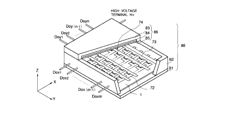
In Fig. 7, 1 denotes a substrate and 73 and 74
respectively denote X- and Y-wires while 74 and 75
respectively designate a surface-conduction electron-
emitting device and a connection. The surface-
conduction electron-emitting device 74 may have a
plannar or stepwise profile.
The substrate 1 is a substrate such as a
glass substrate as described earlier and its
dimensions are determined as a function of its
configuration, the number of devices arranged on the
substrate 1 and, if it constitutes a part of a vacuum
container for the electron source, the vacuum
conditions of the container as well as other factors.
There are a total of m ~-wires 72 designated
respectively as DXl, DX2, ..., DXm, which are
typically made of a conductive metal and formed on the
substrate 1 by vacuum deposition, printing or
sputtering to show a desired pattern, although the
material, the thickness and the width of the wires
need ~o be so determined that a substantially ~.s
equal voltage as possible may be applied to all of
the surface-conduction electron-emitting devices.
On the other hand, there are a total of n
Y-wires 73 designated respectively as DY1, DY2, ...,
DYn, which are also typically made of a conductive
__
3 7 - , is, ~~ '~
1 metal and formed on the substrate 1 by vacuum
deposition, printing or sputtering to show a desired
pattern as in the case of X-wires 72, the material,
the thickness and the width of the wires being so
determined that a substantially as equal voltage as
possible may be appiled to all of the surface-
conduction electron-emitting devices.
The m X-wires 72 are electrically insulated
from the n Y-wires 73 by means of an insulator layer
(not shown) laid therebetween, the X- and Y-wires
forming a matrix. Both m and n are integers.
The insulator layer (not shown) is typically
made of Si02 and formed on the X-wires 72 carrying
substrate 1 by vacuum deposition, printing or
sputtering to show a desired contour, although the
thickness, the material and the technique to be used
for forming it need to be so selected that it may
withstand the largest potential difference at the
crossings of the X- and Y-wires. It may be so
arranged that an insulator layer is found only on and
near the crossings of the X- and Y-wires. With such
an arrangement, a connection 75 and an X~- or Y-wire'
may be electrically connected without using a contact
hole. Each of the X- and Y-wires is Zed out to an
external terminal.
While n Y-wires 73 are laid on m X-wires 72
with an insulator layer interposed therebetween in the
3$ -
",~~~'~'~i~u.~.
1. above description, m X-wires 72 may be conversely laid
on n Y-wires 73 with an insulator layer inserted
therebetween. The insulator layer may be used to
form all or part of the step-forming sections of the
step type surface-conduction electron-emitting devices
constituting the electron source if such electron--
emitting devices are used.
The oppositely arranged device electrodes of
the surface-conduction electron-emitting devices 74
are electrically connected to the respective X-wires
72 (DX1, DX2, ..., DXm) and Y-wires 73 (DY1, DY2, ...,
DYn) by way of respective connections 75 that are
also made of a conductor metal and formed by vacuum
deposition, printing or sputtering.
Either a same conductor material or totally or
partly different conductor materials may be used for
the m X-wires 72, n Y-wires 73, connections 73 and
oppositely arranged device electrodes. Such materials
may be appropriately selected from metals such as Ni,
Cr, Au, Mo, W, Pt, Ti, A1, Cu and Pd, alloys of these
metals, printing conductor materials constituted of a
metal or a metal:oxide'such as Pd, Au; Ru02, Pd-Ag
and glass and semiconductor materials such as
-w
- 3g _ ;j , c~ ~;~ )
w ~, ~, w a ,L
1 X-wires 72 in order to scan the rows of the surface-
conduction electron-emitting devcie 74 according to -
input signals. On the other hand, modulation signal
generation means (not shown) is connected to the Y-
wires 73 for applying modulation signals to the Y-
wires 73 in order to modulate the columns of the
surface conduction electron-emitting device 74
according to input signals. A drive voltage is
applied to each of the surface-conduction electron-
emitting devices as the difference of the voltage of
the scan signal and that of the modulation signal
applied to the device.
Now, an image-forming apparatus comprising an
electron source having a configuration as described
above will be described by referring to Figs. 8 and
9A and gB, of which Fig. 8 schematically
illustrates the configuration of the image-forming
apparatus and Figs. gA and 9B illustrate two types
of fluorescent films that may be used for the
apparatus.
In Fig. 8, the apparatus comprises among
others'an electron source substrate 1, on which a
number of electron-emitting devices are arranged, a
rear plate 81 for securely holding the electron source
substrate l, a face plate 86 prepared by arranging a
fluorescent film 84 and a metal back 85 on the inner
surface of a glass substrate 83 and a support frame
._.1 ,--1
d v
1 82, casing 88 of the apparatus being formed by
applying frit glass to the contact areas of the rear
plate 81, the support frame 82 and the face plate 86
and burning them in ambident air or in a nitrogen
atmosphere at 400 to 500°C for more than ten minutes
to tightly bond them together. Note that reference
numeral 74 in Fig. 8 denotes an electron-emitting region
of the device of Figs. 1A and 1B and reference numerals
72 and 73 respectively designate X- and Y-wires
connected to the pair of device electrodes of related
surface-conduction electron-emitting devices. The
wires connected to the device electrodes of a device
may also be referred to as the device electrodes of
that device hereinafter, if they are made of a
material same as that of the proper electrodes.
While the casing structure 88 is constituted
of the face plate 86, the support frame 82 and the
w
41 - ~ ~ ~~. ~ ~~ _~
1 according to the invention. The fluorescent film 84
of Fig. 8 is constituted only of a number of fluo-
rescent materials if the apparatus is designed as a
monochrome display, whereas it is constituted of
fluorescent materials 92 and a black conductor member
91 which is made of a black conductor material and
may be called a black strip or black matrix depending
on the shape and arrangement of the fluorescent
materials.
Such a black strip or black matrix is arranged
in order to make the space for preventing color mixing
of the fluorescent materials 92 for three primary
colors and suppress any reduction in the contrast of
the image on the face plate of the apparatus that can
be given rise when external light is reflected by the
surface of the face plate.
While graphite is typically used for the
black strip, any other materials may suitably be used
so long as they are electrically conductive and show
low transmissivity and reflectivity to light.
The fluorescent material 83 are formed on the
glass'substrate 83 by printing or precipitation
regardless if the apparatus is a monochrome or Golor
display. A metal back 85 is normally arranged on the
inner surface of the fluorescent film 84 because it
reflects light directed to the inner surfaces.of the
fluorescent materials, operates as an electrode for
42 _
sc 5
;_
1 applying a voltage to electron beams to accelerate
their speed and protects the fluorescent materials
from being damaged by negative ions that are generated
inside the casing to collide with the fluorescent
materials. After the fluorescent film is prepared and
its inner surface is smoothed (in a process normally
called "filming"), the metal back is formed thereon
by depositing aluminum by means of vacuum deposition.
A transparent electrode (not shown) may be
formed on the outer surface of the fluorescent film
84 in order to raise the conductivity of the
fluorescent film 84.
Mote that care should be taken to exactly
align the fluorescent materials of each primary
color and the respective corresponding electron-
~~.~~!~c?~.
1. approximately 10-6Torr by means of an ordinary vacuum
system comprising a rotary pump or a turbo pump.
However, in order for the surface-conduction electron-
emitting devices to show an MI characteristic for the
device current If and the emission current Ie for the
purpose of the invention, an additional process of
baking them in a ultra high vacuum system comprising
an ion pump at 80°C to 150°C for three to fifteen
hours needs~preferably to be carried out after the
forming operation.
A Better operation may be carried out on the
casing 88 in order to ensure a high degree of vacuum
for it after it is sealed. In this operation, a
Better arranged at a given position (not shown) in
the casing 88 is heated by resistance or high
frequency heating to form a film by vapor deposition
before. the casing is hermetically sealed. The Better
is normally made of a material containing Ba as a
principal ingredient and the inside of the casing is
held to a degree of vacuum between 1x10⁻⁵ and
1x10⁻⁷Torr because of the adsorption effect of the
vapor deposited film:
With an image-forming apparatus having a
configuration as described above, images are
displayed on the screen by apglying a voltage to the
electron-emitting devices via the external terminals
Doxl through Doxm and Doyl through Doyn to cause them
r.~
_ ~~ _ ~~~~~~~_
I. to emit electrons, applying a high voltage greater
than several kilovolts to the metal back 85 or the
transparent electrode (not shown) via a high voltage
termianl Hv to accelerate the electrons in order to
make them collide with the fluorescent film 84, which
is consequently energized to emit light to produce
images on the screen.
While some of the structural and functional
features of an image-forming apparatus according to
the invention are described above, the materials and
the configurations of the components of the apparatus
are not limited to those described and other materials
and configurations may alternatively be used whenever
appropriate.
Now, some recommendable drive methods for
driving an electron source or an image-forming
apparatus according to the invention will be described.
According to a first drive method, said scan
signal application means for applying scan signals is
so designed as to apply a voltage V1[V] to wires
selected from the m X-wires and another voltage V2[V]
to the remaining X-wires so that the surface-
conduction electron-emitting devices connected to the
wires to which the voltage V1[V] is applied are
selectively scanned. (V1[V] is not equal to V2[V].)
On the other hand, said modulation signal generation
means generates a pulse-shaped voltage having a given
-w
- ~5 - ~~~~ti~~~x'~.~
1 legnth for the n Y-wires and changes its peak level
(referred to as Vm[V]) for each and every one of the
n Y-wires according to the input signal for that Y-
wire, which may be, for instance, a signal representing
the brightness level of an incoming image signal, in
order to modulate the brightness of the displayed
image.
More specifically, the absolute value of the
drive voltage Vm-V1[V] applied to the selected N
electron-emitting devices that are currently being
scanned is modulated on the basis of the relationship
between the Vf and ze of the electron-emitting devices
so that each and every electron beam may be emitted
from any of the devices with a required intensity
depending on the corresponding input signal, e.g.,
the brightness level of the corresponding incoming
video signal.
Meanwhile, the absolute value of the drive
voltage Vm-V2[V] applied to the remaining electron-
emitting devices that are currently not being
scanned is so controlled as to never exceed a
threshold voltage Vth predetermined for the electron-
emitting devices. Thus, only the electron beams from
the electron-emitting devices being scanned and
hence having respective required intensities are
output for a given period of time, whereas the
remaining electron-emitting devices do not output any
fi
1 electron beams during that period.
According to a second drive method, said scan
signal application means for applying scan signals is
so designed as to apply a voltage V3[V' to wires
i1 .~, /Z ~ .
mu .,.~ . ~ :.~ .;t c:~
- 47 -
1 the corresponding incoming image signal, by modulating
the pulse width Pw[S] of each pulse individually.
Meanwhile, the absolute value of the drive
voltage Vm-V2[V] applied to the remaining electron-
emitting devices that are currently not being scanned
is so controlled as to never exceed a threshold
voltage Vth predetermined for the electron-emitting
devices. Thus, only the electrons emitted from the
electron-emitting devices being scanned and hence
having respective required electric charges are output,
whereas the remaining electron-emitting devices do
not output any electron beams.
According to a third drive method, said scan
signal application means for applying scan signals
1.5 is so designed as to apply a voltage V5(V] to wires
selected from the M X-wires and another voltage
V6[V] to the remaining X-wires so that the surface-
conduction electron-emitting devices connected to the
wires to which the voltage V5(V] is applied are
selectively scanned. (The difference between VS[V]
and V6[V] needs to meet a certain condition.)
On the other hand, said modulation signal
generation means generates a pulse-shaped voltage for
the N Y-wires and changes the timing of applying the
pulse-shaped voltage or its peak level or both for
each and every one of the N Y-wires as a function of
the input signal to modulate the degree of brightness
~"'1
- 48 -
1. in the image being displayed. (Here, the timing of
applying the pulse-shaped votlage means the pulse
width or the phase of the pulse relative to the
corresponding scan signal or both.)
More specifically, the drive voltage applied
to the selected N electron-emitting devices that are
currently being scanned is a voltage pulse whose
pulse width and peak value are modulated and it is so
controlled that the electric charge of each electron
emitted during the scanning period of each and every
one of the electron-emitting devices has a quantity
that matches the corresponding input signal, e:g.,
the brightness level the corresponding incoming video
signal. '.;:
Meanwhile, the drive voltage to the remaining
electron-emitting devices that are currently nod
be~.ng scanned is so controlled as to never exceed a
threshold voltage Vth predetermined for the electron-
emitting devices. Thus, only the electron beams from
z0 the electron-emitting devices being scanned and hence
having respective required intensities are output for
the duration of the time scanning operation, whereas
the remaining electron-emitting devices do not output
any electron beams during that period.
Incidentally, when an electron source or an
image-forming apparatus according to the invention
comprises surface-conduction electron-emitting devices
- 49 -
1 that are provided with the above described
fundamental feature that both the device current If
and the emission current Ie of the device are sub-
stantially linearly proportional to the voltage
applied thereto, no electron beams would be emitted
from those devices that are not currently being
scanned. Contrary to this, however, when the
emission current Ie of such surface-conduction
electron-emitting devices is monotoneously increasing
to the voltage applied thereto but their device
current If has a VCNR characteristic, electron beams
may possibly be emitted from those electron-emitting
devices that are not currently being scanned. This
may be because, while th;e drive voltage Vm[V]-V2(V] is
applied to the electron=emitting devices that are
not currently being scanned, these device change
their state so that somehow the drive voltage exceeds
the threshold voltage level Vth.
In the following, a divided drive method for
driving an electron source or an image-forming
apparatus according to the invention will be
described.
Referring to Fig. 10, it shows an apparatus
comprising electron-emitting device rows (X1, X2, ...)
each having a plurality of electron-emitting devices
T1 and modulation electrode columns (Y1, Y2, ...)
arranged to form an X-Y matrix. Voltage Vf is
- 5° -
1 applied to one of the electron-emitting device rows
(X1, X2, ...) with a level sufficiently high far
causing the devices of the row to emit electrons
while a voltage is applied to one of the modulation
electrode columns (Y1, Y2, ...) with a level that
varies as a function of the input information signal
to define an electron beam emission pattern for that
electron-emitting device row as a function of the
information signal. Then, this operation is repeated
on a one-by-one basis for all the electron-emitting
device rows to define an electron beam emission
pattern for a frame and the operation of defining an
electron beam emission pattern for a frame is repeated
for a multitude of frames. Then, an image is formed
for a frame by irradiating the image-forming member
of the apparatus with beams in accordance with the
defined electron beam emission pattern and this image
forming operation is repeated for a multitude of
frames.
It should be noted for the above drive method
that, when a voltage is applied to one of the
modulation electrode columns (Y1, Y2, ..:) with a
level that varies as a function of the input
information pattern, a cutoff voltage is applied to
a modulation electrode (which may be, for instance,
assumed to be Y2 here) to which an ON-state voltage
is applied and its neighboring modulation electrodes
~~ ~ ~
ff r
- 51 -
1 (Y1, Y2) regardless of what information signal is
given. Consequently, the modulation electrodes Yl
and Y3 are held to a constant voltage level.
With such an arrangement, by applying a cutoff
voltage, electron beams that are emitted and collide
with the image-forming member are not adversely
affected by the voltage applied to the neighboring
modulation electrode columns. Additionally, any
crosstalks among electron beams are effectively
suppressed.
In a preferred mode of carrying out the above
described drive method, an information signal is fed
to every n-th modulation electrode columns so that
the signal input operation is carried out n+l times
while a cutoff signal is fed to the remaining
modulation electrodes that are not give any infor-
mation.signal.
Referring to Fig. 10, an input signal is fed
to all the even number modulation electrode columns
for ,the first time and then to all the odd number
modulation electrode columns for the second time,
whereas a cutoff 'signal is fed to all the odd number
modulation electrode columns firstly and then to all
52 - ~~~~s ~ ~'r~~.
". b a ~.
1 the modulation electrode volumns (Y1, Y2, Y3, ...) is
firstly 1) fed to modulation electrode columns Yl, Y3,
Y5, ... while a cutoff signal is fed to modulation
electrode columns Y2, Y4, Y6, ... and then secondly 2)
fed to modulation electrode columns Y2, Y4, Y6, ...
while a cutoff signal is fed to modulation electrode
columns Y1, Y3, Y5, ... to define an electron beam
emission pattern for row Xl according to the infor-
mation signal. Then, this operation is repeated for
all the electron-emitting device rows on a one-by-one
basis to define an electron beam emission pattern for
a frame. The operation of defining an electron beam
emission pattern for a frame is repeated for a
multitude of frames. Thereafter, an image is formed
for a frame by irradiating the image-forming member
of the apparatus with beams in accordance with the
defined electron beam emission pattern and this image
forming operation is repeated for a multitude of
frames.
In order to effectively irradiate the image-
forming member of the apparatus with electron beams
emitted from the electron source according to a
defined electron emission pattern, an appropriate
voltage must be applied to the image-forming member
2S as a function of the level of the ON-state voltage
and that of the cutoff voltage as well as the type of
the electron-emitting devices involved.
~,
,,
- 5 3 - ~ ~~. ~. ,~ ~1 v
1 While an information signal (modulation signal)
to be used for the purpose of the invention contains
an ON-state signal which is a voltage signal for
allowing irradiation of the image-forming member with
electron beams beyond a given rate and a cutoff signal
for blocking irradiation of the image-forming member
with electron beams, it may additionally contain a
voltage signal far varying the rate of electron beam
irradiation of the image-forming member if images are
to be formed with a multitude of tones. The ON-state
signal and the cutoff signal are defined as a function
of the type of the electron-emitting devices involved
and the level of the voltage applied to the image-
forming member.
An electron source or an image-forming
apparatus according to the invention and operated by
the above drive method may comprise an image-foaming
member prepared by arranging red (R), green (G) and
blue (B) fluorescent bodies.
The divisor to be used for the drive method
1 a sufficient emission of electrons if a cutoff signal
is not used. Tn case of not feeding a cut off signal,
the X1, X2, .., side can be divided for simultaneous
driving, in place of the Yl, Y2, ... side.
Now, preferred embodiments of electron source
and image-forming apparatus of the present invention
will be described.
Fig. 11 is an exploded and enlarged perspective
view of a combination of an electron-emitting device
to and a face plate of an image-forming apparatus that
comprises a plurality of surface-conduction electron-
emitting devices as illustrated in Fig. 8, sand view
showing several tracks of electron beams emitted from
the electron-emitting device.
- 55 -
1 electrodes 5 and 6 by means of a device drive power
source 10, electrons are emitted from the electron-
emitting region 3 in the form of a beam and accelerated
by acceleration voltage Va applied to the fluorescent
material 84 via the metal back 7 by an electrode
acceleration power source 11 until they collide with
the fluorescent material 84 to cause the latter to
luminesce and form a luminous spot 9 on the face plate
86.
Fig. 12 is a schematic enlarged illustration
of a luminous spot 9 observed by the inventors of the
present invention in an apparatus shown in Fig. 11.
It was found that, as seen in Fig. 12, a
luminous spot of a fluorescent material is expanded
to a certain extent both in the direction of voltage
application of the device electrodes (X-direction)
!'1 ,~
6 - ~ ~y ~ ~~ .
t.x s;
~~..>~ ,.
1 directions, those that are directed to the high
potential device electrode (in positive X-direction)
get to the tip 18 of the luminous spot and those that
axe directed to the low potential device electrode
5 (in negative X-direction) arrive at the tail 19 of
the luminous spot to produce a certain width along X-
direction. since that the luminance of the luminous
spot is low at the tail, it may be safely assumed that
the electrons emitted toward the low potential device
electrode are very small in number.
It was also found by a number of experiments
1
_ ,~ ~ ~. ;~ ~n a i.
1. Differently stated, the electrons emitted from
an electron-emitting region 3 are inevitably deflected
to a certain extent by the voltage Vf applied thereto
for acceleration immediately after the emission.
After looking into the size of the luminous
spot 9 and the electrons deflected from the vertical
axis of the electron-emitting region 3 into X-
direction and other phenomena, the inventors of the
present invention came to believe that the deviation
of the front end of the luminous spot from the axis
of the electron-emitting region (~X1 in Fig. 11) and
that of the tail of the luminous spot from the axis
_ 58
1. Referring to Fig. 13, since it was discovered
in a series of experiments conducted by the inventors
of the present invention that, while the electric
field is swerved near the electron-emitting region
by the voltage applied to the device electrodes and
therefore electrons are accelerated also in X
direction, the voltage applied to the image-forming
member is sufficiently greater than the voltage
normally applied to the electron-emitting device and
consequently electrons are accelerated in X-direction
only near the electron-emitting region and thereafter
move in that direction at a substantially constant
speed. Thus, the deviation in X-direction of the
electron can be obtained by replacing V in equation
(1) with a formula for expressing the X-direction
velocity of an electron after it has been accelerated
near the electron-emitting region.
If the X-direction velocity component of an
electron is C (eV) after it has been accelerated in
X-direction near the electron-emitting region 3, C
is -a parameter that is to be modified by voltage Vf
applied to the device. Thus, ~f C is expressed
as a function of Vf, or C(Vf) (unit being eV) and
the latter is used for equation (1), equation (2)
below can be obtained for displacement ~XO.
0X0 = 2H iC~ Va) ... (2)
Equation (2) above expresses the displacement
,'°v
- 5 9 ' ~ ~ :~. ~ ~l
1. of an electron that is emitted from the electron-
emitting region with an initial X-direction velocity
of 0 and given an X-direction velocity of C (eV) near
the electron-emitting region under the influence of
voltage Vf applied to the device electrodes.
In reality, the initial velocity of the
electron has various directional components including
the X-direction component. If the initial velocity
has a quantity of v0 (eV), from equation (1) the
largest and smallest displacements of an electron
beam in X-direction will be expressed by equations
(3) and (4) below respectively.
L1X1 = 2H~((C + v0)/Va) ... (3)
0X2 = 2H~((C - v0)/Va) . ... (4)
Since v0 can also be assumed to be a parameter
whose value changes depending on voltage Vf applied
to the. electron-emitting region and both C and v0 are
functions of Vf, the following equations containing
constants K2 and K3 can be obtained.
~((C + v0)(Vf)) = K2 Vf and
~((C - v0)(Vf)) = K3~
By modifying equations (3) and (4) and using
the above formulas, equations (5) and (6) below can
be produced.
OX1 = K2 x 2H,~(Vf/Va) ... (5)
~X2 = K3 x 2H~(Vf/Va) ... (6)
where H, Vf and Va are measurable quantities and so
-s
n
- '~~ I~Li~:at
,~ :~. .. ,r,~ .. ..
1 are ~X1 and ~X2.
As a result of a number of experiments where
the quantities of 4X1 and 4X2 are observed, varying the
values of H, Vf and Va, the inventors of the present
invention obtained the following values for K2 and K3.
K2 = 1.25 ~ 0.05 and
K3 = 0.35 ~ 0.05
The above values hold particularly true when
accelerating electric field strength (Va/H) is not
lower than 1kV/mm.
From the above empirical achievements, the
quantity (Sl) of the voltage applied (in X-direction)
to an electron in the electron beam spot on the image -
forming member is expressed by a simple formula as
shown below.
S1 = OX1 - ~X2.
If K1 = K2 - K3, then equation (7) below is
obtained from equations (5) and (6) above.
S1 = K1 x 2H~(Vf/Va) .. (7)
where 0.8 ~ K1 = 1Ø
As far the size of the electron beam spot
in a direction perpendicular to the direction of the
voltage applied to the electron-emitting xegion (Y-
direction), while electrons are emitted with an
initial velocity of v0 also in that direction, they
would not be practically not accelerated in the
direction at all. Thus, the displacement of the
°
61 -
1. electron beam will be expressed by
t1Y = 2Hd(v0/Va) , , , (g)
for both positive and negative Y-directions.
From equations (3) and (4),
~((~X12 - 0X22)/2) - 2H~(v0/Va) ... (9)
--v
_ 62 _ ~:y.r; ~ ~, ..,) .3
~i?~.4 ..~~ep°-~ a! ~ ~~,! ..~.
1. On the basis of the above equations, the
inventors of the present invention went on the study
of the behavior of electron beams emitted from a
number of electron-emitting regions on the image-
s forming member.
In a system illustrated in Fig. 11, emitted
electrons get to the image-forming member to form an
asymmetrical pattern there under the influence of a
swerved electric field in the vicinity of the device
electrodes (Fig. 13) and the edges of the electrodes
as typically shown in Fig. 12.
This phenomenon of a deformed electron beam
spot and an asymmetrical pattern can give rise to a
problem of degraded image resolution to such an
extent that can render characters, if displayed,
practically illegible and severely blur any moving
images:
The contour of an electron beam spot illus-
trated in Fig. 12 is asymmetrical relative to X-
axis and the amount with which its tip or tail is
displaced from the axis perpendicular to the
electron-emitting region can be obtained'by using
equations (5) and (6) respectively. The inventors of
the present invention discovered that a highly
symmetrical luminous spot can be achieved when a
plurality of electron-emitting regions provided
between a higher potential electrode and a lower
-w
63 -
ro .,lt. ~ ~~
1. potential electrode, which surrounds the higher
potential electrode and may be divided into a
plurality of lower potential electrode pieces, are
arranged with a distance D defined by equation (13)
below for separating adjacent sections along the
direction of voltage application and made to hit a'
same spot on the image-forming member.
K2 x 2Hd(Vf/Va) '= D/2 '-_ K3 x 2Hd(Vf/Va)
... (13)
where K2 and K3 are constant and K2 = 1.25 ~ 0.05 and
K3 = 0.35 ~ 0.05.
As for a direction perpendicular to the
direction of voltage application (Y-direction),
electron-emitting regions may well be arranged with
pitch P as defined by inequality (14) belaw if the
electron beam spot formed by electrons emitted from
those electron-emitting regions is required to show
a high degree of continuity and if each of the
electron-emitting regions has a length of L.
p < L + 2K4 x 2H~(Vf/Va) ... (14)
where K4 = 0.80.
If, to the contrary, the electron beam spot'
formed by electrons emitted from electron-emitting
regions having a length of L is required to show
discontinuity, they may well be arranged in Y-
direction at pitch P that satisfies formula ('15)
below.
.-.
t. ~ i
1. P ? L + 2K5 x 2H~(Vf/Va) ... (15)
where K5 = 0.90.
the concept of the present invention can be
used for not only image-forming apparatuses but also
for light sources that can replace the light emitting
diodes of a conventional optical printer comprising a
photosensing drum and light emitting diodes. Note
that, if such is the case, not only linear electron
beams but also two-dimensionally expanded flux of
electron beams may be realized by selectively
utilizing the m row wires and n column wires of an
electron source having a configuration as described
earlier.
Now, some preferably embodiments of such
apparatus will be described below.
25
- 65 - ~ , rAz
w ~ :.-.~
1 (Embodiment 1)
This embodiment is an electron source of an
image-forming apparatus, which is realized by forming
a number of plane type surface-conduction electron-
s emitting devices on respective insulator interlayers
laid on substrates arid using a same material or a
material containing a same element for all the device
electrodes, the X-wires, the Y-wires and the connections
connecting the device electrodes and the wires of the
apparatus.
Fig. 14 shows a plan view of part of the
embodiment of electron source. Fig. 15 illustrates a
cross sectional view taken along line A-A' in Fig. 14.
Figs. 16A through 17H illustrate different steps of
operation of manufacturing such an electron source.
Note that same reference symbols are commonly used to
respectively designate same components in Figs. 14
through 17H. w
More specifically, 1 denotes a substrate and
72 denotes an X-wire corresponding to DXm in Fig. 7
(also referred to as underwire) whereas 73 denotes a
Y-wire' that corresponds to DYn ix~ Fig. 7: 4 denotes a
thin film including an electron-emitting section and 5
and 6 denote respective device electrodes whereas 111
and 112 respectively denote an insulator interlayer and
a contact hole to be used for electrically connecting
the device electrode 5 and the underwire 72.
_ 66 - , ,,~,~~ ? ~ ~a
w ~ la e) ~.
1. This embodiment is prepared through the steps as
illustrated in Figs. 16A through 17H and described
below only for an electron-emitting device and related
parts.
Step a:
A silicon oxide film is formed on a cleansed
soda lime glass plate to a thickness of 0.5um by
0
sputtering,to produce a substrate 1, on which a 50A
o ..
thick Cr layer and a 6,OOOA thick Au layer are
sequentially formed by vacuum deposition. Thereafter,
photoresist (AZ 1370 available from HECHST) is applied
thereto by a spinner and baked. Then, the photoresist
layer is exposed to light with a photomask arranged
thereon and photochemically developed to produce a
resist pattern for an underwire 72. Subsequently,
the Au and Cr deposited layers is wet-etched, using the
resist. pattern as a mask to produce an underwire 72
(Fig. 16A).
Step b:
An insulator interlayer 111 of silicon oxide
is formed to a thickness of O.lum by RF sputtering
(Fig. 168).
Step c:
A photoresist pattern 112 is formed on the
silicon oxide film produced in step b and this _
insulator interlayer 111 is etched, using the
photoresist pattern as a mask, to produce a contact .
- 67 _
1. hole 112 (Fig. 16C).
RIE (Reactive Ton Etching) and CFA arid H2 gases
are used for the etching operation in this step.
Step d: ' y:'
Subsequently, another photoresist pattern is
prepared (photoresist RD-2000N-41: available from
Hitachi Chemical Co., Ltd.) for device electrodes 5 and
0
6 and an inter-electrode gap G and then a 50A thick Ti
0
film and a 1,OOOA thick Ni film are sequentially
formed by vacuum deposition. The photoresist pattern
is dissolved in an organic solvent and the Ni and Ti
deposit films are lift-off to produce device electrodes
5 and 6, which have a width W1 fo 300um and separated
from each other by a distance G of Sum (Fig. 16D).
Step a:
Still another photoresist pattern is formed
for an overwire 73 on the device electrodes 5 and 6 and
then a 50A thick Ti film and a 500A thick Au film are
/1,
G?~ f
1 an inter-electrode gap and its neighboring areas. Using
°
this mask, a 1,000A thick Cr film 121 is formed by vapor
deposition and subjected to a patterning operation.
Then, organic Pd (ccp 4230 available from Okuno
Pharmaceutical Co., Ltd.) is applied thereon by means
of a spinner and heated at 300°C for 10 minutes for
baking. (Fig. 17F).
The formed thin fine particle film 2 which is
made of fine particles of Pd as a main element and
used fox producing an electron-emitting section has a
thickness of 100A and a sheet resistance of 5x10⁴S2/cm2.
The term "a fine particle film" as used herein refers
to a thin film constituted of a large number of fine
particles that may be loosely dispersed, tightly
arranged or mutually and randomly overlapping (to form
an island structure under certain conditions).
Step g:
The Cr film 121 and the baked thin film 2 for
an electron-emitting section are etched; using an acid
etcharit, to produce a desired pattern (Fig. 17G).
Step ha
A pattern is formed so that resist may be
applied to all the surface areas except the contact
hole 112 and; using this as a mask, a 50A thick Ti film
'25 and a 500A thick Au film are sequentially formed by
vacuum deposition. Unnecessary portions of these
films are removed by lift-off and used to fill the
_ 69 _ a c~ :,
~:~ ~~T ~,~,
1 contact hole 112 (Fig. 17H).
Thus, an underwire 72, an insulator interlayer
111, an overwire 73, a pair of device electrodes 5 and
6 and a thin film 2 for an electron-emitting section
are formed on an insulator substrate 1.
Now, a display apparatus incorporating such an
electron source will be described below by referring
to Figs. 8, 9A and 9B.
Firstly, the substrate 1 carrying thereon a
large number of plane type surface-conduction electron-
emitting devices is rigidly fitted onto a rear plate
81. Then, a face plate 86 (comprising a glass substrate
83 and a fluorescent film 84 and a metal back 85
-
1 devices.
The fluorescent film 84 is constituted only
by fluorescent bodies if it is used for a monochrome
display, whereas it comprises in this embodiment a
number of stripe-shaped fluorescent bodies separated by
black stripes of a popularly used black material
containing graphite as a principal ingredient. The
fluorescent stripes are formed on the glass substrate
83 by applying a fluorescent material in the form of
slurry.
An ordinary metal back 85 is arranged on the
inner surface of the fluorescent film 84. It is
prepared by smoothing the inner surface of the fluo-
rescent film 84 (in an operation normally called
"filming") and forming an A1 film thereon by vacuum
deposition.
While a transparent electrode (not shown) may
be farmed on the outer surface of the fluorescent
film 84 in arder to raise the conductivity of the
fluorescent film 84, such a layer is not formed in
this embodiment because the metal back 85 has a
sufficiently high conductivity.
Care should be taken to accurately align each
set of color fluorescent bodies and an electron-
emitting device, as a color display is involved,
before the above listed components of the display
apparatus are bonded together.
~1 -
1. The glass container prepared in a manner as
described above and camprising a glass substrate 83 and
other components is then evacuated by way of an
exhaust pipe (not shown) and a vacuum pump to achieve
a sufficient degree of vacuum in the container and then
a voltage is applied to the device electrodes of the
electron-emitting devices 74 by way of external
terminals Doxl through Doxm and Doyl through Doyn to
carry out a forming operation in order to produce an
electron-emitting region out of the thin film for an
electron-emitting region of each electron-emitting
device. Fig. 4 shows the wavefarm of a pulse voltage
to be used for a forming operation.
In Fig. 4, T1 and T2 respectively indicate the
pulse width and the distance separating adjacent pulses
of a pulse voltage, which are respectively 1 millisecond
and l0.milliseconds for this embodiment, while the
peak level (peak voltage in the forming operation) of
the voltage is lOV. The forming operation is conducted
in a vacuum atmosphere of approximately 1x10 ~Torr for
60 seconds.
The electron=emitting region prepared in a
manner as described above contains fine particles made
of palladium as a main element and having a mean
2S particle size of 30A that are dispersed throughout
that section.
Then, the exhaust pipe is heated by a gas
- 72 -
1 burner until it is molten to hermetically seal the
evacuated casing with a degree of vacuum of approxi-
mately 10 6.
Finally, a getter operation is carried out by
high frequency heating in order to maintain that
degree of vacuum within the casing after it is sealed.
An image-forming apparatus according to the
invention and having a configuration as described
above is operated by using signal generating means
(not shown) and applying scan signals and modulation
signals to the electron-emitting devices by way of
the external terminals Dxl through Dxm and Dyl through
Dyn to cause the electron-emitting devices to emit
electrons. Meanwhile, 5kV is applied to the metal
back 85 by way of high voltage terminal ~Iv to
accelerate electron beams and cause them to collide
with the fluorescent film 84; which by turn is
energized to emit light to display intended images.
In order to accurately understand the
performance of a plane type surface-conduction
electron-emitting device according to the invention,
an experiment was' carried out, in which a sample of
plane hype surface-conduction electron-emitting
device was prepared for comparison according to the
same process as the electron-emitting device used in
the above and tested for its properties by using a
measuring apparatus provided with a normal vacuum
1 system as shown in Fig. 3. Values same as those of a
device according to the invention were selected
respectively for Ll, W1, W2 and other variables shown
in Fig. 1. For the test of the sample, the distance
between the anode electrode arid the electron-
emitting device was 4mm and the anode voltage was
lkV, while the inside of the vacuum chamber of the
gauging system was maintained to a degree of vacuum
of 1x10⁻⁶Torr. The device voltage applied to the
device was raised uniformly at a rate of approximately
1V/sec to increase monotoneously both device current
If and electron emission current Ie.
The device current If and the emission current
Ie were measured while applying the device voltage to
the device electrodes 5 and 6 of the sample for
comparison to prove a current-voltage relationship
illustrated in Fig. 5. (Sae Fig. 19). To the
contrary, in a test using an electron-emitting device
according to the invention, the emission current Ie
showed a rapid increase when the device voltage
exceeded 8V and reached to l.2uA when the device
voltage was 14V, at which the device current If was
2.2mA so that an electron emission efficiency n
(=Ie/Ifx100($)) of 0.05 was obtained. Since a device
changes its characteristics depending on the environ- _
mental factors including measuring and vacuum condi-
tions, care was taken to carry out the experiment
- ~4 - ~~.~~ ~~~t~~.
1. under same arid constant conditions.
(Embodiment 2)
This embodiment is an electron source of an
image-forming apparatus, which is realized by forming
a number of step type surface-conduction electron-
emitting devices on respective substrates and using
a same material or a material containing a same element
for all the device electrodes, the X-wires, the Y-
wires and the connections connecting the device
electrodes and the wires of the apparatus. This
apparatus is characterized in that each electron-
emitting device has an insulator interlayer which is
laid between its X-wires and Y-wires and constitutes a
raised section of the device.
Since each electron-emitting device and related
parts of the electron source have a plan view same as
that of Fig. 14, it will not be described here any
further. Fig. 20 shows a cross sectional view taken
along line A-A° in Fig. 14. Ln Fig. 20, there are
shown a substrate l., an X-wire 72 (also referred to
as overwire) that corresponds to Dxm in Fig. 7, a
Y-wire 73 (also referred to as underwire) that corre-
sponds to Dym in Fig. 7, a thin film 4 including an
electron-emitting section, a pair of device electrodes
5 and 6 and an interlayer lll.
This embodiment is prepared by following the
steps described below and illustrated in Figs. 21A
- 75 -
1 through 21F.
Step a:
0
A 5,OOOA thick Pd layer is formed on a cleansed
soda lime glass substrate and then photoresist (AZ
1370 available from HECHST) is applied thereto by a
spinner and baked. Then, the photoresist layer is
exposed to light with a photomask arranged thereon
and photochemically developed to produce a resist
pattern for a Y-wire 73. Subsequently, the Pd film
was etched to produce a Y-wire 73 and a device
electrode 5 simultaneously (Fig. 21A).
Step b:
An insulator interlayer 111 of silicon oxide
is formed to a thickness of 0.1~m by RF sputtering.
Said interlayer is laid between an X-wire 72 and a
Y-wire and serves as a raised section of the surface-
conduction type standing electron-emitting device
(Fig. 21B).
Step c:
A photoresist pattern 112 is formed on the
silicon oxide film produced in step b for a step
section 57 having'a desired profile and an insulator
interlayer 111 and then the insulator interlayer 111
is etched, using the photoresist pattern as a mask,
to produce a raised section 67 with a desired profile
and have the insulator interlayer 111 conform to the
designed shape (Fig. 21C).
1
- 76 - ~~,~i~~ ~
1. RIE (Reactive Ion Etching) and CF4 and H2
gases are used for the etching operation in this step.
Step d:
Subsequently, another photoresist pattern is
prepared (photoresist RD-2000N-41: available from
Hitachi Chemical Co., Ltd.) for device electrodes 5
°
and 6 and a wire 75e and then a 1,OOOA thick Pd is
formed by vacuum deposition. The photoresist pattern
is dissovled in an organic solvent and the Pd deposit
film is lift-off to produce oppositely arranged device
electrodes 5 and 6, which are separated by a distance
equal to the thickness of the raised section 67 or
l.5um. The device electrode shows a width W1 of
500um. (Fig. 21D).
Step e:
Using a mask having an opening for the device
electrodes 5 and 6 and their neighboring areas as in
°
the case of Embodiment 1 above, a 1,OOOA thick Cr film
121 is formed by vapor deposition and subsequently
subjected to a patterning operation. Then, organic
Pd (ccp 4230 available from Okuno Pharmaceutical Co.,
Ltd.) is applied thereon by means of a spinner and
heated at 300°C for 10 minutes for baking.
The formed thin fine particle film 2 which is
made of fine particles of Pd as a main element and
used for producing an electron-emitting section has
0
a thickness of 100A and a sheet resistance of
'"' --\
_ 77 _
1 5x10~S2/cm2. Then, the Cr film 121 and the baked thin
film 2 for an electron-emitting section are etched,
using an acid etchant, to produce a desired pattern
(Fig. 21E).
Step f:
An Ag-Pd conductor body is formed on the
device electrode 6 to a thickness of approximately
l0um to form an X-wire 72 having a desired contour
(F.ig. 21F).
Thus, an X-wire 72, an insulator interlayer
111, a Y-wire 73, a pair of device electrodes 5 and 6
and a thin film 2 .for an electron-emitting section are
formed on an insulator substrate 1.
Then, a display apparatus incorporating such
an electron source is formed in a manner similar to
that of Embodiment 1.
In order to accurately understand the
performance of a step type surface-conduction electron-
emitting device according to the invention, an
experiment was carried out, in which a sample of plane
type surface-conduction electron-emitting device was
prepared for comparison according to the same process
as the electron-emitting device used in the above and
tested for its properties by using a gauging apparatus
provided with a normal vacuum system shown in Fig..3 _
as in the case of Embodiment 1. Values same as those
of a device according to the invention were selected
78
1 for the sample.
The device current Tf and the emission current
Ie were measured while applying the device voltage to
the device electrodes 5 and 6 of the sample to obtain
a current-voltage relationship illustrated in Fig. 5
(See Fig. 19).
In test using an electron-emitting device
according to the invention, the emission current Ie
showed a rapid increase when the device voltage
i0 exceeded 7.5V and reached to l.2uA when the device
voltage was 14V, at which the device current If was
2.2mA so that an electron emission efficiency n
(=Ie/If(~)) of 0.048 was obtained.
An image-forming apparatus according to the
invention and having a configuration as described
above is operated by using signal generating means
(not shown) and applying scan signals and modulation
signals to the electron-emitting devices by way of the
external termianls Dxl through Dxm and Dyl through
Dyn to. cause the electron-emitting devices to emit
electrons. Meanwhile, 5kV is applied to the metal
back 85 by way of'high voltage terminal Hv to
accelerate electron beams and cause them to collide
with the fluorescent film 84, which by turn is
energized to emit light to display intended images.
(Embodiment 3)
This embodiment is an electron source of an
-79-
image-forming apparatus, which is realized by forming
a number of plane type surface-conduction electron-emitting
devices on respective substrates and insulator
interlayers between respective X-wires and Y-wires,
said insulator interlayers being found only on and
near the crossings of the X- and Y-wires, connections
for the X- and Y-wires and the corresponding device
electrodes being electrically linked without using
contact holes and arranged directly on the respective
substrates.
Fig. 22 shows a plan view of part of the
embodiment of electron source. Fig. 23 illustrates a
cross sectional view taken along line A-A' in Fig. 22.
Note that same reference symbols are commonly used to
respectively designate same components in Figs. 22 and
23. In Figs. 22 and 23, there are shown a substrate 1,
an X-wire 72 (also referred to as overwire) that
corresponds to Dmx in Fig. 7, a Y-wire 73 (also
referred to as underwire) that corresponds to Dmy in
Fig. 7, a thin film 4 including an electron-emitting
region, a connection 76 and a pair of device
electrodes 5 and 6.
This embodiment is prepared by following the
steps described below and illustrated in Figs. 24A
through 24E.
Step a:
A silicon oxide film is formed on a cleansed
_--w
_r ~ ~:~ ,;1
- ~ ~ .:,.. ..~r
1 Soda lime glass plate to a thickness of 0.5um by
0
sputtering to produce a substrate l, on which a 50A
0
thick Cr layer and a 6,000A thick Au layer are
sequentially formed by vacuum deposition. Thereafter,
photoresist (AZ 1370 available from HECHST) is applied
thereto by a spinner and baked. Then, the photoresist
layer is exposed to light with a photomask arranged
thereon and photochemically developed to produce a
resist pattern for device electrodes 5 and 6, a
connection 75 and a Y-wire 73. Subsequently, the Au
and Cr deposit layer is wet-etched, using the resist
pattern as a mask to produce device electrodes 5 and
6 (electrode width: 300um, interelectrode distance:
2um), a connection 75 and a Y-wire 73 simultaneously
(Fig. 24A).
Step b:
An insulator interlayer 111 of silicon oxide
to be arranged only on and near the crossing of a
Y-wire 73 and an X-wire 72 is formed to a thickness
of O.lum by RF sputtering (Fig. 24B)~
Step c:
A photoresist pattern 112 for an'insulator
interlayer 111 to be arranged on and near the crossing
of a Y-wire 73 and an X-wire 72 is formed on the
silicon oxide film produced in Step b and the insulator
interlayer 111 is etched, using the photoresist
a H ~ r.~~ ::~ Ci
1. 111 having a desired form (Fig. 24C).
RIE (Reactive Ion Etching) and CF4 and H2
gases are used for the etching operation in this
step. ., ..
Step d:
Subsequently, another photoresist pattern is
prepared (photoresist RD-2000N-41: available from
Hitachi Chemical Co., Ztd.) for an X-wire 72 and then
Au was deposited thereon by vacuum deposition to a
a
thickness of 5,OOOA. Thereafter, the photoresist
.v
emt ~, c
,a
82
1 Then, the Cr film 121 and the baked thin film 2
for an electron-emitting region are etched, using an
acid etchant, to produce a desired pattern (Fig.
24E).
Thus, an underwire 72, an insulator interlayer
111, an overwire 72, a pair of device electrodes 5 and
6 and a thin film 2 for an electron-emitting region
are formed on an insulator substrate 1.
Then, a display apparatus incorporating such
an electron source is formed in a manner similar to
that of Embodiment 1.
In order to accurately understand the per-
formance of a plane type surface-conduction electron-
emitting device according to the invention, an
experiment was carried out, in which a sample of plane
type urface-conduction electron-emitting device was
prepared for comparison according to the same process
as the electron-emitting device used in the above and
tested for its properties by using a gauging apparatus
provided with a normal vacuum system shown in Fig. 3
as in the case of Embodiment 1. Values same as those
of a device according'to the invention were selected '
for the sample.
The device current If and the emission current
~~ ~.~!~ '.~
1 Fig. 5.
In an test using an electron-emitting device
according to the invention, the emission current Ie
- 84 - ~ ~ u.3.
1 and to which the first and second drive methods are
respectively applied.
Otherwise, each unit of this embodiment has a
configuration same as that of Embodiment 1 and hence
can be manufactured in a way same as that of Embodiment
1. The forming operation and the operation of bonding
together the face plate, the support frame and the rear
plate to produce a casing for each unit are also same
as their counterparts of Embodiment 1. It should be
noted here, however, a pair of identical apparatuses
axe prepared at the same time for this embodiment.
The casing of one of the prepared apparatuses
is evacuated by means of an ordinary vacuum system to
a degree of vacuum of approximately 10~6Torr and then
the exhaust pipe of the casing is heated and molten
by a gas burner (not shown) to hermetically seal the
casing.: This apparatus is referred to herein as
display panel A. .
On the other hand, the other apparatus is held
by a pair of plate-shaped heat sources at the face and
rear plates respectively and the entire apparatus was
heated and baked at approximately 120°C for an hour: '
Then, the apparatus was evacuated by means of a super
high vacuum system for ten hours while it is heated
continuously: Subsequently, the exhaust pipe of the
casing is heated and molten by a gas burner (not
shown) to hermetically seal the casing. This
_,.
_ g5 _ ~ '?_1
1 apparatus is referred to herein as display panel B.
Finally, both the display panels A and B are
subjected to a Better process using a resistance
heating technique in order to maintain an intended
degree of vacuum after they are sealed.
Now, a drive circuits for driving the panels
A and B for display operation respectively by using
the first and second drive methods will be illustrated
and described below.
Fig. 25 is a block diagram of a drive circuit
for carrying out the first and second drive methods
which are designed for image display operation using
NTSC television signals. In Fig. 25, reference numeral
1701 denotes display panel A or B prepared in a manner
as described above. Scan circuit 1702 operates to scan
display lines whereas control circuit 1703 generates
input signals to be fed to the scan circuit. Shift
register 1704 shifts data for each line and line memory
1705 feeds modulat~.on signal generator 1707 with data
for a line. Synchronizing signal separation circuit
1706 separates a synchronizing signal from an incoming
NTSC signal. Both Vx and Va in Fig. 25 denote a DC
voltage source.
Each component of the apparatus of Fig. 25
operates in a manner as described below.
The display panel 1701 is connected to external
circuits via terminals Dxl through Dxm, Dyl through Dym
'y
a
- as -
1 and high voltage terminal Hv, of which terminals Dxl
through Dxm are designed to receive scan signals .for
sequentially driving on a one-by-one basis the rows
(of n devcies) of a multiple electron beam source
in the apparatus comprising a number of surface-
conduction electron.-emitting devices arranged in the
form of a matrix having m rows and n columns.
On the other hand, terminals Dyl through Dyn
are designed to receive a modulation signal for
controlling the output electron beam of each of the
surface-conduction electron-emitting devices of a row
selected by a scan signal. High voltage terminal Hv
is fed by the DC voltage source Va with a DC voltage
of a level typically around lOkV; which is sufficiently
high to energize the fluorescent bodies of the selected
surface-conduction electron-emitting devices.
The scan circuit 1702 operates in a manner as
follows.
The circuit comprises n switching devices
(of which only devices S1 and S2 are schematically
shown in Fig. 25), each of which takes either the
output voltage of the DC voltage source or OV and
comes to be connected with one of the terminals Dxl
through Dxm of the display panel 1701. Each of the
switching devices S1 through Sm operates in accordance
with control signal Tscan fed from the control circuit
1703 and can be prepared by combining transistors
- 8 7 - ~ ~. 3 ~ ix ~ ~.
1 such as FETs.
The DG voltage source Vx of this embodiment is
designed to output a constant voltage of 7V so that
any drive voltage applied to devices that are not
being scanned is reduced to less than threshold
voltage Vth. (This will be described later in greater
detail by referring to Fig. 28.)
The control circuit 1703 coordinates the
operations of related components so that images may
be appropriately displayed in accordance with _
externally fed video signals. It generates control
signals Tscan, Tsft and Tmry in response to synchro-
nizing signal Tsync fed from the synchronizing signal
separation circuit 1706, which will be described
below. These control signals will be described later
in greater detail by referring to Fig. 30.
The synchronizing signal separation circuit
1706 separates the synchronizing signal component and
the luminance signal component form an externally fed
NTSC television signal and can be easily realized
using a popularly known frequency separation (filter)
circuit. Although a synchronizing signal extracted
from a television signal by the synchronizing signal
separation circuit 1706 is constituted, as well known,
of a vertical synchronizing signal and a horizontal
synchronizing signal, it is simply designated as Tsync
signal here for convenience sake, disregarding its
_ as -
~, component signals. On the other hand, a luminance
signal drawn from a television signal, which is fed to
the shift register 1704, is designed as DATA signal.
The shift register 1704 carries out for each
line a serial/parallel conversion on DATA signals
that are serially fed on a time series basis in
accordance with control signal Tsft fed from the
control circuit 1703. In other words, a control
signal Tsft operates as a shift clock for the shift
register 1704.
A set of data for a line that have undergone
a serial/parallel conversion Band correspond to a
set of drive data for n electron-emitting devices)
are sent out of the shift register 1704 as n parallel
signals Idl through Idn.
Line memory 1705 is a memory for storing a set
of data for a line, which are signals Idl through Idn,
for a required period of time according to control
signal Tmry coming from the control circuit 1703. The
stored data are sent out as I'dl through I'dn and fed
to modulation signal generator 1707.
Said inodulation'signal generator 1707 is in
fact a signal source that appropriately drives and
modulates the operation of each of the surface-
conduction electron-emitting devices and output
signals of this device are fed to the surface-
conduction type electron-emitting devices in the
- 89 -
1 display panel 1701 via terminals Dyl through Dyn.
The display panel 1701 is driven to operate in
manner as described below.
As described above by referring to the embodi-
ments and Fig. 5, an electron-emitting devices according
to the present invention is characterized by the
following features in terms of emission current Ie.
Firstly, as seen in Fig. 5, there exists a clear threshold
voltage Vth (8V for the electron-emitting devices of the
embodiment under consideration) and the device emit
electrons only a voltage exceeding Vth is applied thereto.
Secondly, the level of emission current Ie
changes as a function of the change in the applied
voltage above the threshold level Vth also as shown in
Fig. 5, although the value of Vth and the relationship
between the applied voltage and the emission current may
vary depending on the materials, the configuration and
the manufacturing method of the electron-emitting device.
More specifically, when a pulse-shaped voltage
is applied to an electron-emitting device according to
the invention; practically no emission current is gener-
ated so far as the applied voltage remains under the'
threshold level, whereas an electron beam is emitted once
the applied voltage rises above the threshold level.
It should be noted here that the intensity of
an output electron beam can be controlled by changing the
peak level Vm of the pulse-shaped voltage.
- 90 -
1. Addtionally, the total amount of electric charge
of an electron beam can be controlled by varying the
pulse width Pw.
Thus, the first drive method can be carried out
for the display panel of this embodiment by using a
voltage modulation type circuit for the modulation signal
generator 1707 so that the peak level of the pulse shaped
voltage may be modulated according to input data, while
the pulse width is held constant.
On the other hand, the second drive method can
be carried out for the display panel of this embodiment by
using a pulse width modulation type circuit for the
modulation signal generator 1707 so that the pulse width
of the applied voltage may be modulated according to
input data, while the peak level of the applied voltage
is held constant.
As each component of the embodiment has been
described above in detail by referring to Fig. 25, the
operation of the display panel 1701 will now be discussed
here in detail by referring to Figs. 26 through 29 and
then the overall operation of embodiment is described.
Fox the sake of convenience of explanation, it
is assumed here that the display panel comprises 6x6
pixels (or m=n=6), although it may be needless to say
that by far much mare pixels are used for a display
panel in actual applications.
The multiple electron beam source of Fig. 26
- 91 -
1 comprises surface-conduction electron emitting devices
arranged and wired in the form of a matrix of six rows
and six columns. Far the convenience of description,
a (X, Y) coordinate is used to locate the devices.
Thus, the locations of the devices are expressed as, for
example, D(1, 1), D(1, 2) and D(6, 6).
In the operation of displaying images on the
display panel of the embodiment by driving a multiple
electron beam sources as described above, an image is
divided into a number of narrow strips, or lines as
referred to hereinafter, running in parallel with the
X-axis so that the image may be restored on the panel
when all the lines are displayed there, the number of
lines being assumed to be six here. In order to drive a
row of electron-emitting devices that is responsible for
an image line, OV is applied to the terminal of the
horizontal wire corresponding to the row of devices,
which is one of Dxl through Dx6, while 7V is applied to
the terminals of all the remaining wires. In synchronism
with this operation, a modulation signal is given to each
of the terminals of the vertical wires Dyl through Dy6
according to the image of the corresponding line.
Assume now that an image as illustrated in Fig.
27 is displayed on the panel and all the bright spots,
or pixels, of the panel have an identical luminance,
which is equal to 100fL (footLambert). While known
fluorescent material P-22 is used for the above display
1~~.~'~
92 _ ~ ~ ~.
1. panel 1701 comprising surface-conduction electron-
emitting devices having the above described features,
to which a voltage of lOkV is applied, and the image
on the panel is updated at a frequency of 60Hz, a
voltage of 14V is most suitably applied for l0usec. to
the electron-emitting devices for a display panel
having 6x6 pixels in order to achieve a luminance of
100fI,. Note, however, that these values are subject to
alterations depending on changes in the parameters.
Assume further that, in Fig. 27, the operation
is currently on the stage of making the third line
turn bright. Fig. 28 shows what voltages are applied
to the multiple electron beam source by way of the
terminals Dx1 through Dx6 and Dyl through Dy6. As
seen in Fig. 28, a voltage of 14V which is by far
above the threshold voltage of 8V for electron emission
is applied to each of the surface-conduction electron-
emitting devices D(2, 3) D(3, 3) and D(4, 3) (black
devices) of the beam source, whereas 7V or 0V is applied
0 to each of the remaining devices (7V to shaded devices
and OV to white devices). Since these voltages are
lower than the threshold voltage of SV, these devices
do not emit electron beams at a11.
In the same way, the multiple electron beam
source is driven to operate for all the other lines _
on a time series basis in order to produce an image
of Fig. 27. Fig. 29 shows a waveform timing chart
~~.~~~~u.~_
1. for the above operation.
As seen in Fig. 29, 'the lines are driven
sequentially, starting from the first line and the
operation of driving all the lines is repeated at a
rate of 60 times per second so that images may be
displayed without flickering.
Images may be displayed in different gradations
by modulating the luminance of each pixel in a manner
as described below, although the above described image
is a monotone image.
With a first method of multiple tone display
involving modulation of the luminance of pixels, the
luminance is raised (or lowered) by raising (or
lowering) the voltage peak level of the pulsed
modulation signal applied to a terminal selected from
the terminals Dyl through Dy6 to make greater (or
smaller) than before above the threshold of 14V.
Lf~; for instance, the voltage peak level is
changed stepwise between 7.9V and 15.9V by a step of
0.5V, the luminance of the pixels can. take a total
of seventeen different steps (or tones) including
luminance zero. The number of tones can'be increased
either by extending the voltage limits or by reducing
'the size of each step.
With a second method of multiple tone display,
the luminance of pixels is raised (or lowered) by
making the pulse width greater (or smaller) than
~~ ~'~ ~ . ..
r ,r;. , ' :. : ' , .';.;- - _ . .: : , ' ,, ~. ::
.~ ~ . ~i ,
:~. ~ :~ ~ ~..
1 l0usec..
If, fox instance, 'the pulse width is changed
stepwise between 0 and l5usec,. by a step of 0.5um,
the luminance of the pixels can take a total of
thirty one different steps (or tones) including
luminance zero. The number of tones can be increase
either by extending the pulse width or by employing
a smaller step.
Now, leaving the simplification of using a
multiple electron beam source for 6x6 pixels, the
overall operation of the apparatus of Fig. 25 will be
described by referring to the timing chart of Fig. 30.
In Fig. 30, (1) shows the timing of operation
of luminance signal DATA which is singled out from
an externally fed NTSC signal by the synchronizing
- 95 - e. ~~.)
at respective timings shown in (4).
Control signal Tscan for controlling the
operation of the scan circuit 1702 is shown in (5).
More specifically, when the first line is driven, only
the switching device Sl in the scan circuit 1702 is
held to OV, whereas the other switching devices are
held to 7V. When the second line is driven, only
the switching device S2 is held to OV, whereas the
other switching devices are held to 7V and so on.
In an experiment using the display panels
A and B and the above described operational procedures,
television images were displayed on the panels. As a
result,.it was observed that, while the display panel
B produced clear and satisfactory images, the
fluorescent materials of the display panel A that
were not energized for image display became bright,
although slightly. In an effort to look into this
problem, samples were prepared for the purpose of
comparison and used for the panels A and B. There-
after, the panels were operated for television
display, where the television drive frequency was
used and the device voltage was held below Vth for
both of the panels A and B to observe the electron
emission current Ie and the device current If. As
a result, it was found in the panel A that both the
electron emission current Ie and the device current
If were not held constant and showed a slight
~' '
..' : '..' .; t ',:' ,
~. ~ '~'''
~~::a.
- 96 _
1 increase. This may be because the functional features
of a surface-conduction electron-emitting device
discovered by the inventors of the present invention
were held under a stable condition in the panel B,
whereas they ware unstable in the panel A because of
the drive conditions, the quality of vacuum within the
casing of the panel and other factors.
Although it is not particularly mentioned
above that the shift register 1704 and the line memory
1705 may be either of digital or of analog signal
type so long as serial/parallel conversions and
storage of video signals are conducted at a .given
- , ~ .~. ~ ~ v ..~.
1 signal generator 1707 can be realized by using a
circuit that combines a high speed oscillator, a
counter for counting the number of waves generated by
said oscillator and a comparator for comparing the
output of the counter and that of the memory.
If necessary, an amplifier may be added to
amplify the voltage of the output signal of the
comparator having a modulated pulse width to the level
of the drive voltage of a surface-conduction electron-
emitting device according to the invention.
If, on the other hand, analog signals are used
with the first drive method, an amplifier circuit
comprising a known operational amplifier may suitably
be used for the modulation signal generator 1707 and a
lever shift circuit may be added thereto'i~ necessary.
'As for the second drive method, a known voltage
control type oscillation circuit (VCO) may be; used
with, if necessary, an additional amplifier to be
used for voltage amplification up to the drive voltage
of surface-conduction type electron-emitting device.
Now, two other embodiments of the invention
will be described in terms of the third drive method
that utilizes modulation of both the peak level and
the pulse width of pulse-shaped voltage. Note that
the'display panel of these embodiments are same as
the display panel B of Embodiment 4.
(embodiment 5)
''a
f~~ ~ ... ,,w ;; '~? ~.
- 9 8 - ~ ~~.... ' '
r d ~~:CJ
1 Fig. 32 is a block diagram of a drive circuit
for the third drive method 'that can be used for a
display apparatus according to the invention. Zike
the circuit of Fig. 17 for the first drive method,
it comprises a display panel 1701, a scan circuit 1702,
a control circuit 1703, a shift register 1704, a line
memory 1705, a synchronizing signal separation circuit
1706, a modulation signal generator 1707 and a DC
voltage soruce Va. Vns in the circuit denotes another
DC voltage source and pulse voltage source 2401 is used
to generate pulses as described hereinafter.
Since the components 1701, 1704, 1705, 1706 and
Va are identical with their counterparts of the
circuit of Fig. 25. They will not described here any
further.
The scan circuit 1702 is provided in the inside
with a total of M switching devices S1 through Sm, each
of which is designed to select either the output
voltage of the pulse voltage source 2401 or that of
the DC voltage source Vns and to be electrically
connected with one of the terminals Dxl through Dxm
of the display panel 1701. These switching devices
S1 through Sm operate according to control signal
Tscan from the control circuit 1703 and can be easily
formed by combining switching devices such as FETs.
While the control circuit 1703 coordinates the
operations of related components as in the case of
1 Fig. 25, it additionally takes the role of feeding the
pulse voltage source 2401 with control signal Tpul.
The pulse voltage source 2401 generates a
pulse voltage according to control signal Tpul from
the control circuit 1703 and the timing of generating
a pulse voltage and the waveform of such a pulse
voltage will be described below by referring to Figs.
33(1) through (5).
The modulation circuit 1707 generates signals
for appropriately driving and modulating the operation
of each of the surface-conduction electron-emitting
devices according to image luminance data I'dl
through I'dn. The waveform of its output signals to
be applied to the surface-conduction electron-emitting
devices will be described below also by referring to
Figs. 33(1) through (5).
Fig. 33(1) illustrates the waveform of a pulse
voltage generated by the pulse voltage source 2401.
This pulse voltage source 2401 maintains its output
voltage to 7V while it does not generate any pulse
voltage but comes to generate a pulse voltage under
'the contral of control signal Tpul. The pulse is a
rectangular pulse having a width of 30usec. that
reduces the output voltage to OV as long as the pulse
voltage is being generated.
Fig. 33(2) shows the output voltage of the
DC voltage source Vns. As shown, the voltage source
.
loo - ~~.~~~,~.~.
1 Vns is constantly producing a voltage of 7V if it is
operating. Note that a pulse width of a OV pulse
voltage generated by the pulse voltage source 2401 is
also shown.
Fig. 33(3) illustrate the waveform of a
modulation signal that can be generated by the
modulation signal generator 1707. The modulation
signal generator 1707 maintains its output voltage to
7V while it does not generate any modulation signal
but comes to benerate a modulation signal according
to image luminance data I°dl through I'dn in synchro-
nism with the output pulse of OV of the pulse voltage
source 2401. A modulation signal is formed by
appropriately combining components a, b, c and d as
indicated by dotted lines in Fig. 33(3) according to
the luminance data of the incoming video signal,
The components a, b, c and d are pulses with
respective voltages of llV, 12V, 13V and 14V, each
having a width o~ 5usec. Note that the pulse of Fig.
33(1) has a width exceeding that of a modulation
signal by 5usec. at both the front and rear ends,
these margins may be varied without problem so long as
the modulation signal is located within the pulse
voltage signal.
Now, tine vaaveform of a drive signal fed to a
surface-conduction electron-emitting device will
be described, using the above described signal
- lol -
1 waveforms.
Fig. 33(4) shows the waveform of a drive
voltage that can be applied to a surface-conduction
electron-emitting device when the output of the pulse
voltage source 2401 is selected by the scan circuit
1702. In other words, it is obtained by withdrawing
the waveform of Fig. 33(1) from that of Fig. 33(3).
In Fig. 33(4), components a°, b', c' and d' shown by
dotted lines correspond to respective components a,
b, c and d of Fig. 33(3). If just a component a' is
selected and applied to a surface--conduction electron-
emitting device, that latter emits an electron beam
that continues for 5usec. at a rate of 0.27uA
(momentary current). Similarly, i~ only a.component
b' is selected and applied, an electron beam is
emitted at a rate of 0.37uA. The value of momentary
current of the electron beam emission is 0.49uA for
component c' and 0.66uA for component d'. Since the
intensity of an electron beam emitted by a surface-
conduction electron-emitting device under consider-
ation does not change linearly, it does not exhibit
the same difference for the same voltage difference
applied to the components. For instance, if components
a° and b° are applied, the output of the device is
not equal to that of the device when only component c'
is applied thereto. This means that a total of
sixteen different outputs can be obtained for an
- 10 2 - ~ ~ .~ ~ ~ : D i_
1 electron-emitting device by differently combining
components a' through d' (including a combination
where none of a' through d' are used) sa that the
luminance of the pixel connected to the device can
be modulated in sixteen different ways.
Fig. 33(5) shows the waveform of a drive
voltage of a surface-conduction electron-emitting
device when the output of the DC current source Vns
is selected by the scan circuit 1702, which is
obtained by subtracting the waveform of a DC voltage
shown in Fig. 33(2) from the modulation waveform
of Fig. 33(3). In Fig. 33(5), components a', b', c'
and d' respectively corresponds to components a, b, c
and d in Fig. 33(3), although no electron beam
emission takes place because none of them exceed
the threshold voltage for electron emission (or 8V
in this embodiment).
Each of the surface-conduction electron-
emitting devices of the embodiment is driven in a
manner as described above. Since the overall
operation of the embodiment of display apparatus is
substantially same as that of the embodiment of Fig.
25, it will not be described here any further.
While a modulation voltage is constituted of
four components a, b, c and d for the sake of
convenience in the above description, the number of
components is preferably more than four in actual
-103- ia.~t~~.
1 applications. In general, because of the non-linear
behavior of a surface-conduction electron-emitting
device according to the invention, a total of 2n
gradations can be achieved for a pixel for image
display by using n components (or n different
modulation voltages).
The number of n is preferably greater than
seven for television images.
While each of the components a, b, c and d
has an equal pulse width of 5usec. in the above
description, they may not necessarily have a same and
equal pulse width. Likewise, while the voltage of the
components a, b, c and d increases with an equal
increment of 1V in the above description, they may
alternatively show different increments of voltage.
(Embodiment 6)
Now, a sixth embodiment of the invention will
be described by referring to Figs. 34 and 35(1)
through 45). This embodiment is so designed as to be
driven also by the third drive method, with which the
luminance of each pixel of the display panel of the
embodiment is controlled by the intensity and the
pulse width of the voltage applied thereto.
Fig. 34 is a schematic block diagram of a
drive circuit that can used for the embodiment. Since
it comprises many components that are identical with
their counterparts of the fifth embodiment illustrated
-:
4 - ~ ;~ v ~ %~ ~ ~' ~.
1 in Fig. 32, only those that are different will be
discussed here. In Fig. 34, pulse voltage sources
2601 and 2602 operate respectively according to
control signals Tpull and Tpul2 from control circuit
5 1703 and respectively send out pulse voltages with a
waveform which is not rectangular and therefore
different from that of the pulse voltage source of
Fig. 32. Modulation signal generator 1707 of the
circuit of Fig. 34 generates modulation signals
ZO according to incoming video signals I'dl through
I'dn with a waveform different from its counterpart
of Fig. 32. These waveforms will be described by
referring to Figs. 3541) through (5).
Fig. 35(1) shows. the waveform of a pulse
voltage generated by the pulse voltage source 2601 of
this embodiment. This pulse voltage source 2601
maintains its output voltage to 7V while it does
not generate any pulse voltage but comes to generate
a pulse voltage under the control of control signal
Tpull as shown there. The pulse is a ramp pulse
having a width of 30usec. and linearly decreases its
height from 3V to OV from the moment it starts.
Fig. 35(2) shows the waveform of a pulse
voltage generated by the pulse voltage source 2602 of '
thus embodiment. This pulse voltage source 2602
maintains its output voltage to 7V while it does not
generate any pulse voltage but comes to generate a
' ~/
f
a
- 105 -
1 pulse voltage under the control of control signal
Tpul2 as shown there. The pulse is a ramp pulse
having a width of 30usec. and linearly decreases its
height from 7V to 4V from the moment it starts.
Since the pulses of Figs. 35(1) and (2) are synchro-
nized with each other by the control signals Tpull
and Tpul2, the pulses generated by the two sources
always show a difference of 4V.
Fig. 35(3) illustrates the waveform of a
modulation signal that can be generated by the
modulation signal generator 1707. The modulation
signal generator 1707 maintains its output voltage to
7V while it does not generate any modulation signal
but comes to generate a modulation signal according to
I5 image luminance data T'dl through I'dn in synch~COnism
with the output pulses of the pulse voltage sources
2601 and 2602. A modulation signal is formed by
appropriately combining components a, b, c and d as
indicated by dotted lines in Fig. 35(3) according to
the luminance data of the incoming video signal. Each
of the components a, b, c and d is on its part a
rectangular pulse having a voltage level of 14V and
a pulse width of 5usec. and these components are
applied respectively 5, 10, 15 and 20usec. after
the start of the pulses having a pulse width of 30usec.
shown in Figs. 35 (1) and (2) .
Now, the waveform of a drive signal fed to a
- 106 - ~ "~ ~
1. surface-conduction electron-emitting device will be
described, using the above described signal waveforms.
Fig. 35(4) shows the waveform of a drive
voltage that can be applied to a surface-conduction
electron-emitting device when the output of the pulse
voltage source 2601 is selected by the scan circuit
1702. In other words, it is obtained by withdrawing
the waveform of Fig. 35(1D from that of Fig. 33(3).
In Fig.' 3544), components a', b°, c° and d' shown by
dotted lines correspond to respective components a,
b, c and d of Fig. 35(3) and have a level exceeding
the threshold voltage for electron emission (or 8V
for this embodiment). Therefore, once any of these
are applied to an electron-emitting device, the latter
start emitting an electron beam with an intensity
that depends on the properties of the device. Since
the intensity of an electron beam emitted by the
surface-conduction electron-emitting device does
not change linearly, it does not exhibit the same
difference for all the components a', b°,'c' and d°.
This means that a total of sixteen different outputs
can be obtained for an electron-emitting device by
differently combining components a' through d' so
that the luminance of the pixel connected to the
device can be modulated in sixteen gradations.
On the other hand, Fig. 33(5) shows the
waveform of a drive voltage of a surface-conduction
~"\
a!
107 - ~. ~ ~!:_~ 1.
1 electron-emitting device when the output of the pulse
voltage source 2601 is selected by the scan circuit
1702. Since it does not the threshold voltage for the
electron-emitting device as in the case of Fig. 33(5),
the device would not emit practically nc~ electron beam.
While a modulation voltage is constituted of
four components a, b, c and d for the sake of
convenience in the above description, the number of
components is.preferably more than four in actual
applications as in the case of Fig. 33(3). In
general because of the non-linear behavior of a
surface-conduction electron-emitting device according
to the invention, a total of 2n gradations can be
achieved for a pixel for.image display by using n
components. The number of n is preferably greater
than seven for television images.
Again, while the waveform a signal generated
- 108 - ~~.~,.~~k:~~.
1 components a, b, c and d may have voltage levels and
pulse widths that are different from one another and ,
these components may start irregularly.
Surface-conduction electron-emitting devices of
the type described before beginning the description of
the embodiments are used for the display panel of each
of the above described embodiments that are used by
one of the above described first, second and third
drive methods. While devices of the above identified
type may vary their characteristics (e.g., threshold
- 109 -
~ ~" 'b ~.~ ':~ ~.c-s .'sr.
1 apparatuses. These methods are particularly suitable
for large displays capable of displaying a large
quantity of image data.
A surface-conduction electron-emitting device
and an image-forming apparatus comprising a number of
such devices may be used not only for applications
where they are exposed to the sight of users but also
for those where they axe used as or for light sources
for recording data like light sources for optical
printers.
Additionally, the drive methods of the present
invention may well be used for driving electron beam
- 110 - ~ ,~ Y~ ~ f ,.-. ~ ,;
s
:.1. , .:r:l '.~ r'",Y :],. _ .
1 [Embodiment 7]
This embodiment is directed to an electron
source or an image forming device of the type that
plural electron emitting elements of surface conduction
type (i.e. surface-'conduction electron-emitting devices),
each including a plurality of electron emitting portions,
are arrayed in a matrix pattern, wherein electron beams
from the plural electron emitting portions are superposed
to form a high-quality image on an image forming member.
The electron emitting elements of this embodiment are
constructed as shown in Fig. 36 which illustrates one
element extracted from the plural electron emitting
elements arrayed in a matrix pattern. The image forming
deuice is fabricated in a like manner to the other
embodiments.
Note that a face plate arranged in opposite
relation to a base plate provided with the electron
emitting elements is of the same as that in the other
embodiments.
In this embodiment, after sufficiently washing
an insulating base plate 361, an element wired electrode
373 for an element electrode 362 on the higher potential
side was formed on the base plate by evaporation and
etching to be 1 um thick and 600 um wide using material
containing Ni as a main ingredient. Then, Si02 was
evaporated in thickness of 2 um all over the base plate
surface to form an insulating layer 372.
- 111 - ~~~~il'.~.y_
1 After that, a 100 um-square contact hole was
opened in Si02 over the element wired electrode 373
by etching. Material such as Ni was first evaporated
in the opening only for connection to the element wired
electrode 373 therethrough, and Ni material was then
evaporated in thickness of 0.1 um all over the surface.
Subsequently, the Ni electrode was formed into
a desired pattern by photolithography and etching so
as to form a higher-potential element electrode 362
which is connected to the element wired electrode 373
and a lower-potential element electrode 363 which lies
perpendicularly to the element wired electrode 373
with electrode gaps left on both sides of the higher-
potential element electrode 362 in the direction of
width (i.e., in the X-direction as shown).
Fine particle films are formed in the gaps
between the element electrodes 362 and 363 to serve
as electron emitting regions 364. By applying a desired
voltage to the electron emitting regions 364, electrons
can be emitted similarly to the other embodiments.
With this embodiment thus constructed, by '
setting~an X-dix°ection width (W) of the higher=potential
element electrode 362 between the two electron emitting
portions 364 to 400 um, applying + 14V and 0V respec-
tively to the higher-potential element electrode 362
and the lower-potential element electrode 363 for
emission of electrons, and applying 6 kV to a fluorescent
,~ T a
- 112 - ~~~'x~:~.
1 material on the face plate positioned above the
electrodes through a distance of 2.5 mm, a substantially
circular bright spot was produced with good symmetry.
A diameter of the bright spot was about 500 um~ in
this embodiment.
An electron beam from an electron emitting
element of surface conduction type including one
electron emitting portion produces a bright point being
poor in symmetry on the surface of an image forming
member, i.e., the surface of fluorescent material in
this case. In contrast, with such an arrangement that
a plurality of electron emitting portions axe formed
on both sides of higher-potential one of element
electrodes with a spacing W, expressed by the following
formula, therebetween in the direction of voltage
application, electron beams emitted from the plural
electron emitting portions are superposed into one
beam on the surface of an image forming member, i.e.,
the surface of fluorescent material in this case, to
thereby produce a bright point with good symmetry in
shape, as proved by this embodiment.
K2*2H(Vf/Va)1/2 ? W/2 ? K'3*2H(Vf/Va)1/2
where K2, K3; constants K2 = 1.25 ~ 0.05, K3 = 0.35 ~
0.05
Vf~ voltage applied to element
Vap voltage applied to image forming member
(accelerating voltage)
Y .g /,"
- 113 -
1 H; distance between electron emitting element
of surface conduction type and image forming
member
W; distance between electron emitting regions
[Embodiment 8]
This embodiment is concerned with an arrange-
ment of plural electron emitting element of surface
conduction type arrayed in a matrix pattern. Fig.
37 snows a schematic view of a image forming device
according to this embodiment, Fig. 38 shows an enlarged
perspective view of one electron emitting element
according to this embodiment, and Fig. 39 shows a
sectional vieca taken~along an X-axis of the element.
In this embodiment, electron emitting elements
were fabricated on an insulating base plate 381 as
follows.
A method of fabricating a image display of
this embodiment will first be described.
(1) After washing the insulating base plate
381; element wired electrodes 389 were formed on the
base plate 381 in thickness of 1 um by evaporation
and etching using material containing Ni as a main
ingredient.
(2) Then, an insulating layer 390 of Si02
was formed in -thickness of 2 um all over the surface
of the base plate 381.
(3) Then, a contact hole was bored in a desired
- 114 -
1 position of Si02 by etching and, thereafter, element
electrodes 382 and 383 were formed in thickness of
0
1000 A by evaporation and photolithography. Material
of the electrodes contains Ni as a main ingredient.
(4) As a result of the above step, the element ,.
electrode 382 was electrically connected to the element
wired electrode 389, and both the element electrodes
382 and 383 were positioned in opposite relation with
narrow gaps of 2 um left therebetween. The process
subsequent to a step of forming Pd fine particle films
in the gaps to serve as electron emitting regions 364
is the same as that in the other embodiments and hence
omitted here.
In this embodiment, the element electrodes
382 electrically connected iri the Y-direction and the
element electrodes 383 electrically connected in the
X-direction constitute an XY-matrix with the electron
emitting regions formed in the gaps between both the ..
electrodes. As a result, the plural electron emitting
elements are formed in a matrix pattern.
As shown in Fig. 38, each electron emitting
element includes the electron emitting region 384 on'
both sides of the higher-potential element electrode
382 in the direction of voltage application (i.e.,
in the X-direction). In this embodiment, a width (W)
of the higher-potential element electrode (i.e., device
electrode) in the X-direction was set to 800 um and
''~\ . .
- 115 - ~' a
..:~. ~ ~ ~w~ 3
1 a gap width (G) between the element electrodes 382,
383 was set to 2 um.
Further, a length (L) of the electron emitting
region in the Y-direction was set to 140 um and an
array pitch (P) of the electron emitting elements in
the Y-direction was set to 750 um.
Additionally, an array pitch of the electron .
emitting elements in the X-direction was set to 1 mm
in this embodiment.
Above the insulating base plate 381 on which
the electron emitting elements were fabricated as
explained above, similarly to the other embodiments,
a face plate 388 including a transparent electrode
386 and a fluorescent substance layer (image forming
member) 387 both coated on its inner surface was
positioned via a support frame (not shown) with a
distance d = 4.5 mm therebetween. The base plate,
the support frame and the face plate were bonded
together by applying frit glass to joined portions
between those members and baking the glass at 430°C
for l0 minutes or more.
In the image display thus constructed, an
accelerating voltage Va of 5000 V was applied to the
fluorescent material layer 387 through the transparent
electrode 386 and a voltage Vf of 14V was applied
between the element electrodes 382, 383 through the
element wired electrode 389.
. .. . ~ : . :,: , . ~. w : .: - ., ,~... .. . ~ y;
.
.. ' v , '; , , ~ '- ' , -: " . . . _ ':~
-.. . .;. ;
':~ :; :
~.
~ :. , : .
;_ . . . : ' '..~, " .., -''-. " .'..
b ~,.:, . , w . . . , .~" .. ; :'..::~
;,;... '. '.:: '
~
~
~..,
,.. :. .
.. . . :'. ..'...'. .:, , .,.. :~ :. ~
. . ;.,,._... ,.:: .. .~.. ... . .-..
~ ~ . :.~ ....:
:
' ;_:~.W., .,
-- 116 - ~~:~~~. ~ ~i
1 Specifications of this embodiment were as
follows; accelerating voltage Va = 5000 V, element
voltage Vf = 14V, element/face plate distance d =,4.5
mm, Y-direction length L of electron emitting region
in element = 140 um, Y-direction array pitch P of
electron emitting elements = 750 um, and width of
higher-potential electrode = 800 um. It was observed
as with above Embodiment 7 that electron beams emitted
from the two electron emitting regions substantially
coincided in axes of their luminous spots with each
other on the image forming member, and two bright spots
were superposed in precisely symmetrical relation to
produce one almost circular luminous spot as a whole.
This successful result is inferred to come from
agreement of the conditions in this embodiment with
the formula shown in above Embodiment 7.
Further, as a result of ~.ntensive studies made
by the inventors, it was found that.superposition of
the two luminous spots in the Y-direction can be
controlled by specifying an arrangement of those bright
spots in view of the relationship among variables
expressed by the following formulae.
In case where bright points are continuously
superposed with each other in the Y-direction;
p < L + 2K5*2H(Vf/Va)1/2
where K5; constant K5 = 0.80 Va; accelerating voltage,
/~\v
.~ :~ ,.3. :~ r.~ : ~ ,
1 face plate, L; Y-direction length of electron emitting
region in element; P; Y-direction array pitch of
electron emitting elements; and W; width of higher-
potential electrode.
In case where bright points are not superposed
and discontinuous in the Y-direction:
P ? L + 2K6*2d(Vf/Va)1/2
where K6; constant K6 = 0.90
Thus, it was found that the electron emitting elements
are required to be arrayed in the Y-direction in view
of the conditions of the above formulae. This embodi-
went satisfies the range defined by the latter formula
corresponding to the case where bright points are not
superposed and discontinuous in the Y-direction; hence
the two luminous spots were observed as independent
spots.
According to the image display of this embodi-
ment, as described above, a luminous spot is produced
in an optimum shape, and a highly discernible and
sharper display image is obtained with a high degree
of luminance and fineness.
[Embodiment 9] ,
This embodiment is concerned with an image
forming device that plural electron emitting elements
of surface conduction type, which can be driven in
a divided manner, are arrayed in a matrix pattern,
and a method of driving the device. A description
-_,
a c ~, ,,
- lls - ~~ ~~~a
1 of this embodiment will be given below with reference
to Figs. 40 and 41. Fig. 40 is a perspective view
of a part extracted from an electron source in which
electron emitting elements of surface conduction type
are arrayed in a matrix pattern, and.Fig. 41 is a
circuit diagram showing a driving method of this
embodiment..
In the element of this embodiment, element
electrodes 461a, 461b and wired electrodes 462a, 462b
are respectively connected to each other, as shown
in Fig. 40. 452a denotes a wired electrode.in the X-
direction and 462b denotes a wired electrode in the
Y-direction. The electron source ofthis embodiment
is constructed similarly to above Embodiment 4 such
that electron emitting elements of surface conduction
type corresponding to red (R),~green (G) and blue (B)
are arrayed as shown iw Fig. 41. Though not shown,
an enclosure is also fabricated similarly.
The method of driving the device according
to this embodiment will now be described with reference
to Fig. 41.
Zet it be 'assumed that the matrix'is scanned
successively on a row-by-row basis from M = 1 in Fig.
41.
(1) Voltage applying means (not shown) is
turned on to apply a constant voltage to the transparent
electrode for thereby applying an electron emission
- 119 -
1 ~.S~>
1 voltage Vf to the row M = 1.
(2) Of information signals for one scanned
row (M = 1), information signals to be input to signal
wired electrodes G for green and signal wired electrodes
B for blue are once stored in a memory 48Q. Information
signals to be input to signal wired electrodes R for
red are directly applied, as a modulation voltage (VmR)
taking any one of an ON voltage, a cutoff voltage and
a gradation voltage depending on each information
signal, to the signal wired electrodes R through a
voltage applying means 481. During a period of that
application, cutoff signals are issued from a signal
switching circuit 482 for the signal wired electrodes
G, B regardless of states of the information signals,
whereby a cutoff voltage (Voff) is applied to each
of tlae signal wired electrodes G, B through a voltage
applying means 483.
(3) The signal switching circuit 482 is then.
- 120 - ~~:~~~v~.
1 that application, cutoff signals are issued from the
signal switching circuit 482 for the signal wired
electrodes R, B regardless of states of the information
signals, whereby a cutoff voltage (Voff) is applied
to each of the signal wired electrodes R, B through
the voltage applying means.
(4) The signal switching circuit 482 is then
changed over such that, of the information signals
for one scanned row (M'= 1), the information signals
ZO for blue in the information signals previously stored
in the memory 48 are input to the signal wired electrodes
B: Thus, a modulation voltage (VmB) taking any one
of an ON voltage, a cutoff voltage and a gradation
voltage depending on each information signals is applied
to the corresponding signal wired electrode B through
the voltage applying means 483. During a period of
that application, cutoff signals are issued from the
signal switching circuit 482 for the signal wired
electrodes R, O regardless of states of the,information
signals, whereby a cutoff voltage (Voff) is applied
to each of the signal wired electrodes R, B through
the voltage applying means.
The above operation of applying the information
signals for one scanned row to the respective signal
wired electrodes while dividing the information signals
into threes in timed relation for each color, i.e.,
at every two rows, is carried out within a display
.~ .e r. ~y
- 121 - ~~.~.~r.:~~
1 time allocated for one scanned row.
By repeating the above operations (1) to (4)
successively so as to Scan the rows one by one, one
or more full-color images for one or multiple pictures
are displayed on the surface of the fluorescent material
layer.
According to the driving method of this
embodiment, plural bright spots forming a display image
on the surface of a fluorescent material layer parti-
tinned for respective colors are produced in extremely
uniform and stable size and shape without causing
crosstalk. As a result, a full-color image having
higher color purity and improved color reproduction
is displayed.
[Embodiment 10]
Fig. 42 is a block diagram showing one example
of a display in which a display panel using the above-
mentioned electron emitting elements of surface
conduction type as an electron source is arranged to
be'able to display image information provided from
various image information sources including TV broad-
casting, for example:' In Fig. 42, denoted by 500 is
a display panel, 501 is a driver for the display panel,
502 is a display controller, 503 is a multiplexer,
504 is a decoder, 505 is an input/output interface,
506 is a CPU, 507 is an image generator, 508, 509 and
510 are image memory interfaces, 511 is an image input
/'~\ ' -\
- 122 - ~ ~ ~~
1 interface, 512 and 513 are TV signal receivers, and
514 is an input unit. (when the present display
receives a signal such as a TV signal, fox example,
including both video information and voice information,
it of course displays an image and reproduces voices
simultaneously. But circuits, a loudspeaker and so
on necessary for reception, separation, reproduction,
processing, storage, etc. of the voice information,
which are not directly related to the features of the
present invention will not described here.)
Functions of the above components will be
described below along a flow of image signals.
First, the TV signal receiver 513 is a circuit
for receiving a TV image signal transmitted through
a wireless transmission system in the form of electric
waves or spatial optical communication, for example.
A type of the TV signal to be received is not limited
to particular one, but may be any of the NTSC, PAT
and SECAM types, for example. Another type TV signal
(e.g., so-called high-quality TV signal including the
MUSE type) having the larger number of scan lines than
the above types is a.signal source fit to'utilize an'
advantage of the display panel suitable for an increase
in the screen size or the number of pixels. The TV
signal received by the TV signal receiving circuit
513 is output to the decoder 504.
Then, the TV signal receiver 512 is a circuit
r~
- 123 -
1 for receiving a TV image signal transmitted through
a wire transmission system in the form of coaxial cables
or optical fibers. As with the TV signal rece~.ver
513, a type of the TV signal to be received by the
TV signal receiver 512 is not limited to particular
one, The TV signal received by the receiver 512 is
also output to the decoder 504.
The image input interface 511 is a circuit
for taking in an image signal~supplied from an image
input unit such as a TV camera or an image reading
scanner, for example. The taken-in image signal is
output to the decoder 504.
The image memory interface 510 is a circuit
for taking in an image signal stored in a video tape
recorder (hereinafter abbreviated to a VTR). The.
taken-in.image signal is. output to the decoder 504.
The image memory interface 509 is a circuit
for taking in an image signal stored in a video disk.
The taken-in image signal is output to the decoder
504.
The image memory interface 508 is a circuit
for taking in an image signal from a device storing
still picture data, such as a so-called picture disk.
Tkhe taken-in image signal is output to the decoder
504.
The input/output interface 505 is a circuit
for connecting the display to an external computer
-124- ~, ,,.
1 or computer network, or an output device such as a
printer. zt is possible to perform not only input/
output of image data and character/figure information,
but also input/output of a control signal and numeral
data between the CPU 506 in the display and the outside
depending on cases:
The image generator 507 is a circuit for
generating display image data in accordance with image
data and character/figure information input from the
outside via the input/output interface 505, or image
data and character/figure information output from the
CPU 506. Tncorporated in the image generator 507 are,
for example, a rewritable memory for storing image
data and character/figure information, a read only
memory for storing image patterns corresponding to
character codes, a processor for image processing,
and other~circuits required for image generation.
The display image data generated by the image
generator 507 is usually output to the decoder 504,
but may also be output to an external computer network
or a printer via the input/output interface 505 depending
on cases.
The CPU 506 primarily carries out operation
control of the display and tasks relating to generation,
selection and editing of a display image. For example,
the CPU 506 outputs a control signal to the multiplexer
503 for appropriately selecting one of or combining
'~\
1 ones of image signals to be displayed on the display
panel. In this connection, the CPU 506 also outputs
a control signal to the display panel controller S02
depending on the image signal to be displayed, thereby
appropriately controlling the operation of the display
in terms of picture display frequency, scan mode (e. g.,
interlace or non-interlace), the number of scan lines
per picture, etc.
Further, the CPU 506 directly outputs image
data and character/figure information to the image
generator 50?, or accesses to an external computer
or memory via the input/output interface 505 for .
inputting image data and character/figure information.
It is a matter of course that the CPU 506 may be used
in relation to any suitable tasks for other purposes
than the above. For example, the CPU 506 may directly
be related to functions of producing or processing
information as with a personal computer or a word
processor, or it may be connected to an external
computer network via the input/output interface 505,
as mentioned above, to execute numerical computations
and other tasks in cooperation with external equipment.
The input unit 514 is employed when a user
enters commands, programs, data, etc. to the CPU 506,
and may be any of various input equipment such as a
keyboard, mouse, joy stick, bar code reader, and voice
recognition device.
,.--.1
- 126 -
1 The decoder 504 is a circuit for reverse-
converting various image signals input from 507 to
513 into signals for three primary colors, or a
luminance signal, an I signal and a Q signal. As
indicated by dot lines in the drawing, the decoder
504 preferably includes an image memory therein.
This is because the decoder 504 also handles those
TV signals including the MUSE type, for example, which
require an image memory for the reverse-conversion.
Further, the provision of the image memory gives rise
to an advantage of making it possible to easily display
a still picture, or to easily perform image processing
and editing, such as thinning-out, interpolation,
enlargement, reduction and synthesis of image(s), in
cooperation with the image generator 507 and the CPU
506.
The multiplexer 503 appropriately selects a
display image in accordance with the control signal
input from the CPU 506. In other words,. the multiplexer
503 selects desired one of, the reverse-converted image
signals input from the decoder. 504 and outputs it to
the driver 501. In this connection, by switchingly
selecting two or more of the image signals in a display
time for one picture, different images can also be
displayed in plural areas defined by dividing one screen
like the so-called multiscreen television.
The display panel controller 502 is a circuit
n
127 - ~~~~~~?~~
1 for controlling the operation of the driver 501 in
accordance with a control signal input from the CPU
506. As a function relating to the basic operation
of the display panel, the controller 502 outputs to
the driver 501 a signal for contralling, by way of
example, the operation sequence of a driving power
supply (not shown) for the display panel. As a function
relating to a method 'of driving the display panel,
the controller 502 outputs to the driver 501 signals
for controlling, by way of example, a picture display
frequency and a scan mode (e. g., interlace or non-
interlace).
Depending an cases, the controller 502 may
output to the driver 501 control signals for adjustment
of image quality in terms of luminance, contrast, tone
and sharpness of the display image.
The driver 501 is a circuit for producing a
drive signal applied to the display panel 500. The
driver 501 is operated in accordance with the image
signal input from the multiplexes 503 and the control
signal input from the display panel controller 502.
With the various components arranged as shown
in Fig. 42 and having the functions as described above,
'\
1 decoder 504, and at least one of them is selected by
the multiplexer 503 upon demand then input to the driver
501. On the other hand, the display controller 502
issues a control signal for controlling the operation
of the driver 501 in accordance with the image signal
to be displayed. The driver 501 applies a drive signal
to the display panel 500 in accordance with both the
image signal and the control signal. An image is
thereby displayed on the display panel 500. A series
of operations mentioned above are controlled under
supervision of the CPU 505.
In addition to displaying the image signal
selected from the image memory built in the decoder
504, the image generator 507 and other information,
the present display can also perform, on the image
information to be displayed, not only image processing
such as enlargement, reduction, rotation, movement,
edge emphasis, thinning-out, interpolation, color
conversion, and conversion of image aspect ratio, but
also image editing such as synthesis, erasure,
connection, replacement, and inset. Although not
especially specified in the description of this
embodiment, there may also be provided a circuit
dedicated for processing and editing of voice informa-
tion, as well as the above-explained circuits for image
processing and editing.
Accordingly, even a single unit of the present
- 129 - ~~ ~ ~ ~~ ~
~...!. t :r.L
1 display can have functions of a display for TV
broadcasting, a terminal for TV conferences, an image
editor handling still and motion pictures, a computer
terminal, an office automation terminal including a
word processor, a game machine and so on; hence it
can be applied to very wide industrial and domestic
fields.
It is needless to say that Fig. 42 only shows
one example of the configuration of a display using
a display panel in which electron emitting elements
of surface conduction type are used as electron beam
sources, and the present invention is not limited to
the illustrated~example. For example, those circuits
of the components shown in Fig. 42 which are not
necessary for the purpose of use may be dispensed with.
On the contrary, depending on the purpose of use, other
components may be added. When the present display
is employed as a TV telephone, it is preferable to
provide, as additional components, ~ TV camera, an
audio microphone, an illuminator, and a transmission/-
reception circuit including a modem.
In the present display, particularly, the display
panel using electron emitting elements of surface
conduction type as electron beam sources can easily
be reduced in thickness and; therefore, a depth of
the display can be made smaller. Additionally, since
the display panel using electron emitting elements
- 130 -
1 of surface conduction type as electron beam sources
can easily increase a screen size and also can provide
high luminance and a superior characteristic of
viewing angle, the present display can display a more
realistic and impressive image with good viewability.
[Effect of the Invention]
As described above, by utilizing the following
three features in basic characteristics of the electron
emitting element of surface conduction type according
to the present invention;
first, the element produces the emission current
Ie which is abruptly increases when an element voltage
higher than a certain voltage (called a threshold
voltage, Vth in Fig. 6), but which is little detected
at a voltage lower than the threshold voltage Vth;
namely, it is a non-linear element having the definite
threshold voltage Vth with. respect to the emission
current Ie,
secondly, the emission current Ie depends on
r~
a .~ ~ /~ :~
- 131 - ~~ ~ ~.,R,
1 additionally, in the more preferable case,
both the element current If and the emission current
Ie in the element has a monotonously increasing
characteristic (called an NI characteristic) with
respect to a voltage applied to a pair of element
electrodes facing each other, electrons emitted .from
the electron emitting element of surface conduction
type are controlled with the height and width of a
pulse voltage applied between the element electrodes
facing~each other when the pulse voltage is higher
than the threshold voltage. However, those electrons
are little emitted when the pulse voltage is lower
~~~~''~ ~.
- 132 - ' ~'
1 a pulse having a height, a width, or a height and width
depending on the input signal, and select means, which
may be called scanning means, V for selecting the
electron emitting element row successively one by one
in accordance with the synch signal which is contained
in the input signal:
Thus, according to the novel construction and
driving method of the present invention based on the
characteristics of an electron emitting element of
surface conduction type, there is obtained a high-
quality electron saurce which comprises numerous
electron emitting elements of surface conduction type,
and which can successively select the electron emitting
~\
- 133 -
ii '~
a ,~ ~ t~
1 row wirings and the n lines of column wirings axe
partially or totally the same in their constituent
elements. Therefore, particularly when a high tempera-
ture is applied during manufacture of the device, the
problem of connecting between different kinds of metals
is solved; hence the inexpensive and simple device
structure can be provided with high reliability.
Moreover, since insulating layers are present
only in the vicinity of points where the m lines of
row wirings and the n lines of column wirings cross
each other, and a part or all of the insulating .layers
in the stepped portions of the vertical electron
emitting elements of surface conduction type is
manufactured by the same process, the manufacture
method is simplified in such a point that the m lines
of row wirings or the n lines of column wirings can
be connected electrically to the elements without using
contact holes. As a result, there can be provided
an electron source and an image forming device which
are inexpensive and simple in structure.
According to another driving method of the
present invention,. input signal dividing means for
dividing input signals into plural groups of input
signals is further provided, and plural rows (or columns)
of the electron emitting elements of surface conduction
type are selected and modulated in accordance with
each group of divided plural input signals generated
W\
- 134 - ~~~~L~ ~ i.
1 by the input signal dividing means, thereby providing
a divided driving method. Therefore, a time allowed
for each row (or column) of the electron emitting
elements of surface conduction type can be increased;
hence a driving IC and the electron emitting elements
of surface conduction type can be designed with.greater
allowance.
Further, according to that driving method,
the row (or column) of the electron emitting elements
adjacent to the row (or column) of the electron emitting
elements. being selected and modulated are maintained
in a state under a constant potential applied. There-
fore, no crosstalk occurs between electron beams emitted
from the electron emitting elements on the image forming
~5 member to which the electron beams are irradiated.
According to the electron source of the present
invention, since plural electron beams emitted from
plural electron emitting portions in each electron
emitting, element of surface conduction type are super-
posed with each other, the electron beams can be
controlled into a highly symmetrical shape on the
electron irradiated surface.
Also, by properly specifying the element array
pitch in the Y-direction, it is possible to control
superposition between the electron beams emitted from
the electron emitting elements on the surface to which
the electron beams are irradiated.
- 135 -
a ~ ':f vp
1 As a result, there can be provided an electron
source which can easily select those electron emitting
elements from which electrons are to be emitted and
also control an amount of the emitted electrons with
a simple structure.
The image forming device, e.g., the display,
of the present invention is a device for forming an
image in accordance with input signals, the device
comprising plural electron emitting elements of surface
conduction type cahich are each constituted by at least
element electrodes and thin films inclusive of electron
emitting regions, are arrayed in a matrix pattern on
a base plate corresponding to pixels making up an image,
and the pairs of opposite element electrodes are
respectively connected to m lines of row wirings and
the n lines of column wirings laminated over the former
wirings via insulating layers according to the input.
signal which is cpmposed of synih signals and image
signals, select means for selecting a desired row of
the plural electron emitting elements of surface
conduction type in accordance with the synch signals,
and modulation means for producing modulation signals
depending on the image signals and inputting the
modulation signals to the electron emitting elements
selected by the select means in accordance with the
synch signals. Particularly, the image forming device
includes fluorescent materials which are positioned
- 136 -
1 in opposite relation to a base plate of the electron
source and produce visible lights upon irradiation
of electron beams. Preferably, the image forming device
contains a vacuum therein and has such a feature that
both the element current and the emission current in
each electron emitting element of surface conduction
type exhibits monotonously increasing characteristic
(called an MI characteristic) with respect to a voltage
applied to the pair of opposite element electrodes.
Thus, according to the novel construction and
driving method of the~present invention based on-the
characteristics of an electron emitting element of
surface conduction type there is obtained a device
which includes~an electron source comprising numerous
electron emitting elements of surface conduction type,
which can successively select the electron emitting
elements and control an amount of emitted electrons
in accordance with input signals by applying scan signals
and modulation signals, both obtained from the. input
signals, to m lines of row wirings and n lines of column.
wirings one by one, respectively, without using grid
electrodes which have~been essential in the prior art,
and which can eliminate crosstalk between pixels,
modulate display luminance with good control performance,
and further enables display in finer gradations, making
it possible to display a TV image with high quality,
for example.
- 137 -
1 Also, since the fluorescent materials are
directly excited by the electron beams in a vacuum,
those fluorescent substances in respective colors which
are conventionally well known in the art of CRT and
have superior luminescent characteristics, can be used '.
as light emitting sources. It is therefore possible
to easily realize color display and represent a large
range of hues. Additionally, color display can be
achieved just by separately coating the fluorescent
materials respective colors, and the display panel
can easily be manufactured. Since the voltages required
for scan and modulation are small, electric circuits
can easily be integrated. These advantages cooperatively
make it possible to reduce a production cost and realize
an extremely inexpensive display. As a result, there
can be provided an image forming device such as a display
which can emit lights with brightness selectively
controlled and hence has high display quality.
Further, with the arrangement including_pairs
of opposite element electrodes in the electron emitting
elements of surface conduction type, m lines of row
wirings and n lines of column wirings, at least part
of lines respectively connecting in parallel the pairs
of opposite element electrodes in the electron emitting
elements of surface conduction type, the m lines of
row wirings and the n lines of column wirings are
partially or totally the same in their constituent
-,,
1 members.
The electron emitting elements of surface
conduction type are formed on the base plate or the
insulating layers.
The insulating layers axe present only in the
vicinity of points where the m lines of row wirings
and the n lines of column wirings cross each other,
and a part or all of the insulating layers in the stepped
portions of the vertical electron emitting elements
of surface conduction type is of the same structure.
Because of including the electron source.having
the above structural features, there can be provided
an image forming device which is highly reliable, is
inexpensive, and has a novel structure.
According to another driving method adapted
for the novel image forming device of the present
invention, input signal, dividing means for dividing
input signals into plural groups of input signal is
further provided, and plural rows (or columns) of the
electron emitting elements of surface conduction type
are selected and modulated in accordance with each
group of divided plural input signals generated by
the input signal dividing means, thereby providing
a divisional driving method. Therefore, a time allowed
for each row (or column) of the electron emitting
elements of surface conduction type can be increased;
hence a driving IC and the electron emitting elements .
i~
-139- '~V~~!~~~
~ .e.
1 of surface conduction type can be designed with greater
allowance.
Further, according to that driving method,
the row (or column) of the electron emitting elements
adjacent to the row (or column) of the electron emitting
elements being selected and modulated are maintained
in a state under a constant potential applied. 'there-
fore, no crosstalk occurs between electron beams emitted
from the electron emitting elements on the image forming
member.
According to the image forming device of. the
present invention, since plural electron beams emiated
from plural electron emitting portions in each electron
emitting. element of surface conduction type are super-
posed with each other on the image forming member,
a resulting luminescent bright spot~can be controlled
into a highly symmetrical shape..
Also, by properly specifying the element array
pitch in the Y-direction, it is possible to control
superposition between the electron beams emitted from
the electron emitting elements on the image forming
member, with the result that a high-quality image
corresponding to the input image can be presented.
In addition, since the image forming device
2~ of the present invention can use TV signals, signals
from image input devices, image memories and computers,
etc. as input signals, even a single unit can have
- 140 -
~~,~t~
1 functions of a display for TV broadcasting, a terminal
for TV conferences, an image editor handling still
20