Note: Descriptions are shown in the official language in which they were submitted.
,.
1
PIXEL, CONTROL CIRCUTTRY
FOR SPATIAL, LIGHT MODULATOR
TECHNICAL FIELD OF THE INVENTION
This invention relates to spatial light modulators, especially those known
as deformable mirror devices, and more particularly to circuitry for
controlling
the on and off states of individual pixel elements.
CA 02113213 2003-04-11
2
BACKGROUND C?F THE IhTVEI~TI~C?N
Spatial light modulators (SLMs) consist of an array of electronically
addressable pixel elements and related control circuitry. A typical
application
is for image display, where light from each pixel is magnified and projected
to
a display screen by an optical system. The type of modulation depends on how
the modulator is combined with an optical system.
A frequently used type of SLM is the defo~mable mirror device, in which
each pixel element is a tiny micro-mechanical mirror, capable of separate
movement in response to an electrical input. Incident light may be modulated
in direction, phase, or amplitude for reflection from each pixel.
For many applications, the SLM is binary in the sense that each pixel
element may have either of two states. The element may be off, which means
that it delivers no light. Or, the element may be on, which means that it
delivers
light at a maximum intensity. To achieve a viewer perception of intermediate
levels of light, various pulse width modulation techniques may be used. These
techniques are described in pending U.S. Patent filo. 5,27$,652, entitled
"DMD Architecture and Timing for C7se in a Pure-Width Modulated Display
System", assigned to the same assignee as the present application.
In general, pulse width modulation produces an integrated brightness by
switching each pixel on or off for a period that corresponds to a binary
number,
during each frame. Pulse width modulation uses various schemes for loading the
SLM, such as "bit-frame" loading, in which one bit per pixel for an entire
frame
is loaded at one time. Each pixel element has a memory cell. The entire array
. ~; )3~)3
3
of memory cells is loaded with one bit per cell, then all pixel elements are
set
to correspond to that bit-frame of data. During the display time of the
current
bit-frame, data for the next bit-frame is loaded. Thus, for example, for 8-bit
pixel brightness quantization, the SLM is loaded eight times per frame, one
pixel
per frame at a time. In one such method, the most significant bit is displayed
for 1/2 of a frame period, the second most significant bit for 1/4 frame
period,
etc., with the least significant bit {LSB) representing a display time of
1/2° frame
period, for n-bit brightness quantization.
A problem with existing pixel loading techniques is that they require at
least one memory cell per pixel element. As the number of pixels per frame
increases, the memory requirements for the SLM device results in increased
costs and reduced manufacturing yields. A need exists for an SLM that has
reduced circuitry for controlling the pixel elements.
Loading schemes that use a memory cell for every pixel element also limit
the minimum time in which a pixel element can be set, to the time required to
load a bit-frame into the memory aiTay. When pulse width modulation is used,
the display time for the LSB is the shortest display time. During this LSB
time,
the data for the next frame must be loaded. This is the time period when a
"peak" data rate is required. 'To satisfy this peak data rate, a certain pin
count
and data frequency on those pins must be available. A high peak data rate
translates into a high pin count and/or high frequency, which increases device
and/or system costs. A need exists for an SLM that reduces this peak data
rate.
~A
CA 02113213 2003-04-11
4
SUI~~MARY OF THE INVENTION
A first aspect of the invention is a spatial light modulator (SLM) having
individually controlled pixel elements, each of which rnay be set and reset to
either of two states depending, on a value of a data signal delivered to that
pixel
element. The SLM has an array of pixel elements, each having two possible
states depending on the value of a data signal delivered to it from an
associated
memory cell. The SLM also has a number of memory cells, each in data
communication with a set of pixel elements. Each memory cell stores a data
value representing an on or o:Pf state of a pixel element of its set and
delivers a
signal representing this data value to the pixel elements of its set. A number
of
reset lines are connected to the pixel elements such that a different reset
line is in
communication with each pixel element of a set. rhhus, the reset lines may be
used to reset only one pixel element of a set at a time.
In accordance with one aspect of the present invention there is provided a
method of pulse-width modulating frames of' mufti-bit frame data, comprising
the
steps of: providing a spatial light modulator comprised of an array of pixel
elements, an array of memory cells, and a plurality o k' reset lines, each
memory
cell in communication with a set of pixel elements, each reset line connected
to a
plurality of said pixel elements such that a di fferent said reset line is in
communication with each said pixel element in each said set of pixel elements;
delivering data representing a split bit-frame o.f data to said memory cells,
wherein each memory cell receives a data bit representing an on or off state
of
CA 02113213 2003-04-11
4a
only one of its pixel elements; and resetting said pixel elements associated
with a
reset line, by using a reset signal to allow all pixel elements connected to
said
reset line to change state.
A technical advantage of the invention is that a single memory cell
controls a set of multiple pixel elements. 'This reduces the circuitry per
pixel,
which has the effect of reducing device cost and increasing manufacturing
yields.
Also, the peak data rate at which loading must occur is reduced because there
are
fewer memory cells to load far any one reset. 'This has the effect of reducing
pin-counts and/or lowering data frequency requireznexats, with the further
effect
of lower device and/or systems cast.
21 13?13
s
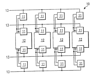
BRIEF DESCRIPTION OF TI-IE DRAWINGS
Figure 1 is a block diagram of a portion of an SLM array, having memory
cells with a fanout of four pixel elements.
Figure 2 illustrates a memory cell having a fanout of four pixels.
Figure 3 illustrates the bistable operation of a mirror element of an SLM.
Figures 4 and 5 illustrate how reset lines can be easily connected for
torsion-hinge type pixel element arrays having conductive mirrors and hinges.
Figure 6 is an example of a data sequence for loading a frame of data into
an array of memory cells, each having a fanout of four pixel elements.
Figures 7-9 illustrate enhanced embodiments for providing improved fault
tolerance.
A
.e
~~~~~~3
6
DETAILED DESCRIPTION OF THE INVENTION
Pixel Array Interconnections
Figure 1 is a block diagram of a portion of an SLM array 10, having pixel
elements 11 that are controlled with memory cells 12 and reset lines 13. Only
a small number of pixel elements 11 with their related control circuitry is
shown;
a typical SLM array 10 would have thousands of such elements 11. Figure 1 is
primarily intended to show how each memory cell 12 serves multiple pixel
elements 11. Additional detail about the interconnections between pixel
elements 11, memory cells 12, and reset lines 13 is explained below in
connection with Figures 2 - 5..
SLM 10 is, for purposes of this description, a device known as a
deformable mirror device (DMD). DMDs have arrays of tiny micro-mechanical
mirror elements, which may be modulated to provide the viewer with a
perception of varying intensity. An example of a DMD is the DMD device
manufactured by Texas Instruments, Inc. However, the invention is not limited
to the use of DMD's for SLM 10, and may be used with other types of SLMs
having addressable pixel elements, with similar characteristics, namely,
operation
in accordance with data signals and a reset control signal, as explained
below.
Pixel elements 11 are operated in a bistable mode, which means that there
are two stable states. As explained below in connection with Figure 3, the
direction of their movement is controlled by "loading" them with data from
their
memory cell 12 via address electrodes to "drive" the pixel element 11. As
711:
2i132~3
further explained in connection with Figure 3, the state of the pixel element
11
is changed, in accordance with this driving voltage, by applying a
differential
bias via a reset electrode. T'he term "reset signal" is used herein to refer
to a
signal that is delivered to the pixel elements 11 to cause them to change
state.
Pixel elements 11 are grouped into sets of four pixel elements 11, each
set in communication with a memory cell 12. The number of pixel elements 11
in a set associated with a single memory cell 12 is referred to as the
"fanout" of
that memory cell 12. Thus, in Figmve l, each memory cell 12 has a "fanout" of
four pixels. The invention is applicable to other fanout values, but a fanout
of
four is used herein for purposes o:f example.
Each memory cell 12 may be a conventional SRAM (static random access
memory) cell. One of the advantages of many of today's designs for SLM 10
is that they may be easily integrated onto underlying CMOS control circuitry.
This description is in terms of memory cells 12, each having a single bit
storage
capacity. However, the scope of the invention could also include "memory
cells" that store more than one bit or that have additional logic circuitry.
For
example, each memory cell 12 could have a double buffer configuration.
Four reset lines 13 control the time when the pixel elements 11 change
their state. Once all memory cells 12 for the pixel elements 11 connected to a
particular reset line 13 have been loaded, the states of the pixel elements 11
change according to the data with which they have been loaded, simultaneously,
in response to a reset signal on that reset line 13. In other words, the pixel
~°~t
t ~ ~ . ~~l 1...
w ~ (f
~~1~~1~
s
elements 11 retain their current state as the data supplied to them from their
memory cell 12 changes, and until receiving a reset signal.
Each pixel element 11 in the set of four pixel elements associated with a
memory cell 12 is connected to a different one of four reset lines 13. Thus,
each pixel element 11 in a set can change its state at a different time from
that
of the other pixel elements 11 in that set.
In general, each set of pixel elements 11 associated with a memory cell
12 has the same number of pixel elements, and this number is the same as the
number of reset lines 13. However, there could be instances, such as on edges
of the pixel element array, where a memory cell 12 is connected to a fewer
number of pixel elements.
Figure 2 illustrates a sex of four pixel elements 1 l, its memory cell 12 and
reset lines 13, and the related interconnections. Each pixel element 11 is
labeled
in terms of the reset line 13 to which it is connected, i.e. pixel element 11
(A)
is connected to reset line 13(A). As indicated, either a "1" or a "0" value
may
be delivered to the pixel elements 11. When the memory cell 12 is switched,
either of those values is delivered to all pixel elements 11 to which that
memory
cell 12 is connected. A signal on the reset line 13 of each pixel element 11
determines whether that pixel element 11 will change state.
Figure 3 is a cross sectional illustration of a single pixel element 11 of a
typical DMD type of SLM 10. The spatial light modulation is provided by a
reflective mirror 31, which tilts in either of two directions. The two stable
states
of mirror 31 are indicated by the dotted lines. In its stable positions, one
end
2i X3213
9
of mirror 31 has moved toward one of two landing electrodes 32. Two address
electrodes 33 are connected to the outputs of the memory cell 12 whose fanout
includes that pixel element 11. A reset voltage is applied to the conductive
mirror 31 by means of a reset electrode 34. Address electrodes 33 are used to
apply a voltage difference, such that one end of mirror 31 is attracted to its
underlying electrode 33 and the other end is repelled. The reset voltage at
electrode 34 determines whether the mirror 31 will actually rotate to the
corresponding landing electrode 32. Thus, the mirror 31 are "loaded" via their
memory cell 12 and reset via reset lines 13. If tilted in a selected
direction, such
as toward a display screen, a pixel element will be "on"; otherwise it is
tilted so
as to direct light elsewhere, such as to a trap.
Figure 4 is a top plain view of a portion of an array of pixel elements 11,
whose reset lines 13 are via torsion hinges 41. As in Figures l and 2 and as
indicated by dotted lines, each pixel element 11 is associated with a memory
cell
12 having a fanout of four pixel elements 11. In this embodiment, pixel
elements 11 have conductive mirrors 31 and conductive torsion hinges 41 so
that
the reset can be applied directly to the mirrors 31 via the hinges 41 without
special connections or isolations. In Figure 4, where each mirror 31 has a
pair
of hinges 41 and where pixel elements 11 are aligned so that the hinges 41 are
along horizontal lines, connections to reset lines 13 are easily made along
these
horizontal lines.
Figure 5 illustrates an alternative arrangement of SLM 10. As in Figure
4, the fanout of each memory cell 12 is a vertically spaced set of pixel
elements
4~ 1
w' ~i i3~1~
to
11. However, the reset connections are along diagonal reset lines 13. As in
Figures 2 and 3, each pixel element 11 is labeled in terms of the reset line
13
to which it is connected, i.e. pixel element 11 (A) is connected to reset line
13(A). This arrangement would be useful in SLMs 10 where it is advantageous
to align pixel elements 11 such that their hinges 41 are along diagonal lines.
Operation of the Invention
For pulse width modulation, the operation of SLM 10 is generally
consistent with existing pulse width modulation techniques in that an n-bit
value
represents the brightness of each pixel element 11 during a frame period. Each
bit of the n-bit value represents a time during which the pixel element 11 is
either on or off. The number of bits in the n-bit value is referred to herein
as
the "bit depth".
For proposes of example herein, it is assumed that each pixel element 11
displays light during one frame in accordance with a bit depth of 5 bits.
Thus,
for example four pixel elements 11 in a set associated with a single memory
cell
12 might have the following data for a single frame:
pixel 1 A B C D E
pixel 2 F G H I ;f
pixel 3 K L M N O
pixel 4 P Q R S T
where {ABODE} represents a 5-bit binary value. The value of each bit is "1"
or "0" representing one of two possible states for the pixel element 11.
A
CA 02113213 2003-04-11
If it is assumed that a "1'" in the LSB position represents an "on" value
of one time unit, then a "1" in the MSB position will represents 16 time
units,
with the intermediate bits ranging downwaxd as requiring 8, 4, and 2 time
units.
If bit 4 is the MSB, and bit 0 is the LSB, the times represented by each a
"1"'
value of bit are:
bit 4 (MSB) 16 time units
bit 3 8 time units
bit 2 4 time units
bit 1 2 time units
bit 0 (LSB) 1 time unit
Thus, the greater the 5-bit value, the longer the pixel element 11 is on
during a
frame, and the brighter it is relative to other pixel elements 11 during that
frame.
Further details about pulse width modulation techniques are described in
U.S. Patent No. 5,278,652, referred to in the background section of this
patent
application.
The pulse width modulation technique described herein makes use of the
fact that some on or off times are long compared to the switching speed
capability of memory cells 12. An underlying premise of the invention is that
a single memory cell 12 may serve multiple pixel elements 11 if its data
loading
is sequenced so that no more than one of its pixel elements 11 needs resetting
at the same time.
In general, the sequencing used to load each frame of data depends on
fanout and the bit-depth. w'ari:ous sequences are possible, but a rule that
the
~t ~3~i3
12
sequencing must follow is that no two pixel elements 11 in a set can need
loading at the same time.
Several "optional" rules, in addition to the rule of the preceding paragraph,
may be applied. Where a fanout of m pixel elements is assumed, one such rule
is that at the beginning of the sequence, all m pixel elements 11 are loaded
in
the first m time units. Thus, each pixel element 11 of each set is loaded in a
continuous series of initial time slices. This rule results in good separation
between frames, with a maximum skew of m time units between the end of one
frame and the beginning of the next. Also, the data loaded during the first m -
1 time slices should not be the LSB data. Finally, the data for any one pixel
element 11 should begin and end in the same position relative to a frame. This
is true because for a bit depth of n bits, the number of data units used for
loading data is 2° - 1 data units.
Figure 6 illustrates an example of data sequencing for a memory cell 12
having a fanout of four, and applying all of the above rules. Thus, where m =
4, and it is assumed that each loading step takes one time unit, the four
pixel
elements 11 associated with a memory cell 12 are loaded with the same data but
only one pixel element 11 is reset. The pixel elements associated with a first
reset line 13(A) are designated as pixel elements 11(A), etc.
The loading sequence of Figure 6 is for 5-bit data frames as follows:
Load pixels 11 (A), bit 4, and reset 13(A)
Load pixels 11(B), bit 3, and reset 13(B)
Load pixels 11(C), bit 2, and reset 13(C)
y1
i~ ~i, , ~''~~,V'~
4
~~?~~13
13
Load pixels 11(D), bit 3, and reset 13(D)
Skip 2 LSB time units
Load pixels 11(C), bit 4, and reset 13(C)
Skip 2 LSB time units
Load pixels 11(B}, bit 0, and reset
13(B}
Load pixels 11(B), bit 1, and reset
13(B)
Load pixels 11(D), bit 1, and reset
13(D)
Load pixels 11(B), bit 4, and reset
13(B)
Load pixels 11(D}, bit 0, and reset
13(D)
Load pixels 11(D), bit 2, and reset
13(D)
Skip 1 LSB time unit
Load pixels 11(A), bit 0, and reset 13(A)
Load pixels 11(A), bit 2, and reset 13(A}
Load pixels 11(D), bit 4, and reset 13(D}
Skip 2 LSB time units
Load pixels 11(A), bit 3, and reset 13(A)
Load pixels 11{C), bit 0, and reset 13(C)
Load pixels 11{C), bit 1, and reset 13(C)
Skip 1 LSB time unit
Load pixels 11(C), bit 3, and reset 13(C)
Skip 2 LSB time units
Load pixels 11(B), bit 2, and reset 13(B)
Load pixels 11{A), bit l, and reset 13(A}
A
~r~~2~3
14
Skip 1 LSB time unit
Buffering with a frame buffer (not shown) may be used to order the data in the
correct sequence. A frame of data (the data that fills an array of SLM 10} is
divided into four "split bit-fraunes". For the first split bit-frame, bit 4
for each
pixel element 11(A) in each set associated with memory cells 12 would be
appropriately ordered for loading during a time unit, such that 1/4 of the SLM
is loaded. Then, all bit 3's for each pixel element 11(B) would be ordered
as a second split bit-frame for loading, etc.
The overall effect of the data sequencing is that, for each frame, the entire
10 array of pixel elements 11 is reset in groups of pixels, rather than all at
once.
Thus, resetting occurs in a "split reset" pattern, i.e., those pixel elements
11
connected to a single reset line 13 are switched at the same time.
Like prior pulse width modulation techniques, it takes 2° - 1 LSB
time
units to display a full n-bit frame. However, each loading step is done with
smaller increments of memory and can therefor be done in less time. In the
example of this description, l./4 of a bit-frame is loaded for every reset
signal.
In other words, four reset signals are used per bit-frame. Each bit-frame,
unlike
those of prior pulse width modulation techniques, may display data from a
different bit.
As a result of the loading technique of the invention, the peak data rats:
is reduced. Also, although loading occurs more frequently per frame, the
higher
valued bits no longer coincide for all pixel elements 11. Thus, there are no
long
" ~i ~~~~~
is
waits during the display time of these higher valued bits. The average data
rate
and the peak data rate more closely converge.
The maximum fanout per memory cell 12 depends on the bit depth.
Where the bit depth is n, the theoretical maximum fanout may be calculated as:
fanoutm~ = 2° - 1
n
The numerator of the above equation represents that there are 2° -
1 time
slices per frame. The denominator indicates that each fanout requires n
events.
Computer programs may be developed and used to determine appropriate
sequences for varying bit depths and fanouts. A rule-based program will
prevent
violations of the above-stated rule that prohibits more than one pixel element
11
in a set from needing resetting at one time, as well as other optional rules.
An enhanced method of the invention combines the above-described "split
reset" process with a "block clearing". Block clearing has been used with
prior
pulse width modulation schemes to avoid the problem of having to load an
entire
bit-frame during a LSB time unit. F'or block clearing, bit-frames are loaded
in
whole multiples of a LSB time unit. A mechanism is provided on the SLM 10
to allow all pixel elements 11 to be quickly "cleared", i.e., switched to an
"off'
state. Thus, those bit-frames whose "on" times are less than the time required
for loading can be given their appropriate weight. The total number of time
units in a frame exceeds the maximum brightness time by the number of time
units used for clearing. Thus, the consequence of having pixel elements 11 in
an "off" state during part of loading is a reduction in optical efficiency of
the
,.
s~...~h>'''~~:...
CA 02113213 2003-04-11
16
SLM 10. The general aspects of block clearing are described in U.S. Patent
No. 5,278,652.
Fault Tolerance
Figure 7 illustrates an enhancement of the SLM 10 of Figures 1 - S,
especially with respect to the interconnections between each memory cell 12
and
the pixel elements 11 in its fanout. A resistive element, in this case a
resistor
71, is included in each data connection for reducing the impact of a failure
at
any one pixel element 11. For example, a short at one of the pixel elements 11
will not cause the rest of the pixel elements 11 in the set to fail.
As stated above, a feature of many SLMs 10 is that they are easily
fabricated using integrated circuit processes. In these types of SLMs 10,
resistors 71 could be fabricated from a polysilicon material. Alternatively, a
highly resistive material could be used for the electrode contact's. Also, as
an
alternative to extra resistive areas ox elements, the entire fabrication level
for
pixel element electrodes, such as the electrodes ~3 of Figure 3, could be made
from a material, such as titanium nitride or titanium oxynitride; having a
high
sheet resistance.
Figure 8 illustrates another fault-tolerant enhancement of SLM 10.
Instead of resistors 71, diodes 81 are used as a resistive element to isolate
a fault
at any one pixel element 11.
~:~ 13~~3
17
Figure 9 illustrates a third fault-tolerant enhancement. Fuses 91 are
designed to "blow" if there is a shorted pixel element 11. Zener diodes 92 or
some other type of breakdown diode provides a high resistance to ground.
Other Embodiments
Although the invention has been described with reference to specific
embodiments, this description is not meant to be construed in a limiting
sense.
Various modifications of the disclosed embodiments, as well as alternative
embodiments, will be apparent to persons skilled in the art. It is, therefore,
contemplated that the appended claims will cover all modifications that fall
within the true scope of the invention.
,:.