Note: Descriptions are shown in the official language in which they were submitted.
CA 02115553 2001-10-25
s
-1-
PLATED COMPLIANT LEAP
BACKGROUND OF TfIE INVENTTnta
The present invention relates to connectors
for mounting integrated circuit packages to circuit
boards. More particularly, the present invention
relates to a micro-miniature resilient support for
supporting an integrated circuit chip or multiple-chip
module (MCM) on a circuit board, and for interconnecting
electrical circuits on a chip or multiple-chip module
to with circuits on the circuit board.
In the past, laadless ceramic chip carriers
(LCCCs) exhibited problems when exposed to harsh
thermally cyclic environments and vibration. Due to the
thermal cycles and vibration, the solder joints which
connected the LCCC to a circuit board degraded and
cracked over time. The degradation and cracking was
caused by stresses and strains which are induced at the
solder joint by temperature cycling. Ultimately, the
solder joints failed both mechanically and electrically
causing failures in the electronic system in which they
were used.
As a result, a compliant electrical interface
between the leadless chip carrier and the circuit board,
suitable for mass production using current surface mount
technology, has been developed. Such an interface is
described in granter detail in the Pai et al U. S. Patent
No.~,g27,611. The curved leads described in the Pai et al
patent serve as an electrically conductive path between
the LCCC and the circuit board. The curved leads also
form a mechanically compliant interface that withstands
the damaging thermal stresses and vibration which
degraded ~~and destroyed solder joints in previous
interfaces.
WO 93/07657 PC~'/US92/08320
..,.
21.1~~~~
-2-
Although the compliant interface described in
the Pai et al patent provides an effective interface
between the LCCC and the circuit board, i~t'is subject to
certain problems. The curved leads in the Pai et al
patent include tangs which carry a solder slug or bead.
During a soldering process, heat is applied to the
solder of the solder slug causing the solder to flow to
form the solder connection between the lead and the
LCCC. The flowing solder tends to run down the curved
lead into the bent portions of the lead. Then, when the
heat is removed and the solder cools, it hardens within
the bent portions of the curved lead. This hardened
solder reduces compliancy of the curved lead thereby
making the interface formed by the lead less effective.
A second problem with the solder slug used on
the leads in the Pai et al patent is their cost.
Forming the tangs and placing the solder slug within the
tangs on the curved leads is a costly assembly step.
Another problem is that if too much solder is
included in the solder slug, the solder runs beyond the
area intended as a solder joint. This excess solder
creates adverse signal characteristics and, in severe
cases, short circuits with adjacent leads or traces on
the circuit board. Consequently, the circuit board must
be carefully cleaned after solder connection. This is
a difficult and expensive process.
In addition, the tangs and solder slugs at the
end of the curved leads were relatively large in
comparison to the lead width. Hence, additional space
was required between adjacent leads limiting lead
density.
Another problem resulted from a two step
assembly process used to mount the LCCCs to a circuit
board. The leads would be soldered first to the LCCC
WO 93/07657 ~ '~ ~ ~ ~ PCT/~JS92/0~320 'a
~f
_3_
and then to the circuit board. Alignment problems
resulted during the second soldering step of soldering
the leads to the circuit board.
In the past, it was also widely thought that
merely solder plating the leads would be ineffective in
providing adequate solder joints in such applications.
It was thought that gravitational forces would pull the
molten solder, which had been plated on the lead, away
from the solder joint during soldering thereby providing
insufficient solder to form the required joint. Thus,
the tangs and solder beads of the prior art tended to be
the trend in manufacturing such devices.
sY of THE IrrvFrirr~orr
The present invention provides mechanical and
electrical connection between a board contact on a
w
circuit board and a chip contact associated with a
circuit chip or the I/O contacts on multiple-chip
substrates and corresponding contacts on a printed
wiring "mother" board. A curved lead is substantially
entirely plated with solder and is formed of a single
piece of conductive material. The curved lead has a
first surface for connection to the chip contact and a
second surface for connection to the board contact. The
first and second surfaces are connected by at least one
curved portion and are arranged to mount the circuit
chip to the circuit board with the solder. The
;;
resulting connection is a compliant connection which
mounts the circuit chip generally parallel to the
surface of the circuit board to which it is being
connected in an arrangement substantially free of
stress.
It has been found that the solder plated
curved leads of the present invention.solve many of the
problems associated with prior curved leads that
WO 93/07657 PCT/1JS92/0~320
.,"
21~~5~3
_~_ .
included a solder slug. For example, by placing a
surface of the curved lead adjacent to a board contact
on a circuit board or a chip contact on a chip, and then
causing the solder to flow, the surface tension of the
solder enhances a capillary action which draws solder to
the location of the desired solder connection. This
capillary action overcomes gravitational forces which
were previously thought to prohibit adequate solder
joint formation with plated curved leads.
zn addition, the curved leads of the present
invention are plated with adequate solder to form a high
quality solder joint but not so much solder that it runs
away from the desired solder joint. Hence, problems
associated with solder bridges, short circuits and
signal quality degradation resulting from eaccess solder
are all significantly reduced.
Also, the leads of the present invention can
be soldered to both the LCCC and the circuit board
simultaneously. This results in a self-aligning joint
substantially free of stress.
Finally, the curved leads of the present
invention are formed and thaw plated. This saves the
assembly step of applying the solder slugs to the tangs
on leads of the prior art. This also results in a
uniform plating on the lead. Thus, the solder plated
curved heads of the present invention are less expensive
to manufacture than the curved leads of the prior art.
sRI~F o~scRI~TIO~a of THE D~AwI~GS
FIG. 1 is a perspective view of ~a chip carrier
connected to curved leads of the prior art.
FIG. 2 illustrates the manner in which a chip
carrier is mounted on a circuit board using a plurality
of curved leads of the prior art.
FIG. 3 illustrates an embodiment of a single
WO 93/07657 ~ ~ ~ ~ ~ ~ ~ PCT/US92l08320
_5_
curved lead of the prior art attached to a support
strip.
,_
FIG. 4A illustrates an embodiment of a single
curved lead of the present invention arranged between a
chip carrier and a circuit board.
FIG. 4B shows a plurality of curved leads of
the present invention formed on a support strip.
FIG. 5A illustrates the manner in which a chip
carrier is mounted on a circuit board using a plurality
of curved leads of the present invention.
FIG. 5B illustrates the manner in which a
multiple chip module (MCM) is mounted on a circuit board
using a plurality of curved leads of the present
invention.
FIG. 6 shows a second embodiment of a curved
lead of the present invention.
FIG. 7 shows a third embodiment of a curved
lead of the present invention.
~'tETAThED DESCRIPTION OF THE PREFERRED EMBODIMENTS
FIG. 1 shows a connector system 10 of the
prior art. Connector system 10 includes a leadless chip
carrier 12 and a plurality of curved leads 14. The
curved leads 14 are shown connected to circuit contacts
16 formed on leadless chip carrier 12. The curved leads
14 are formed in accordance with the process described
in the Pai et al U.S. Patent No. 4,827,611. Thus, the
curved leads provide a compliant mechanical and
electrical contact between an integrated circuit chip
(shown in FIG. 2) inserted in chip carrier 12 and a
circuit board.
FIG. 2 is a side view of connector system 10
showing chip carrier 12, having an integrated circuit
chip 18 inserted within chip carrier.l2. Chip carrier
12 is coupled to a circuit board 20. As described in
WO 93/07657 PC'd'/US92/0832Q
-6_ .
the Pai et al patent, tangs 22 of curved leads 14 hold
a solder bead or slug 24. Curved leads 14 axe soldered
to chip carrier 12 by heating the solder beads 24
causing them to wet and connect with the electrical
contacts 16 of the leadless chip carrier 12. The chip
carrier 12 self-centers on the leads 14 . Thus, the flat
chip carrier 12 makes an intimate mechanical and
electrical contact with the upper surfaces of leads 14.
After leads 14 are attached to the leadless
chip carrier 12, a second operation is necessary to
attach the leadless chip carrier 12, through the
compliant leads 14, to the circuit board 20. The
circuit board 20 has metal plated electrical connections
21. The circuit board 20 mounting pads are coated with
solder and the solder wets to the board 20 forming areas
for mounting the carrier 12. The carrier, with leads
14, is then placed over the contacts on circuit board
20. Carrier 12 maintains the lower portion of leads 14
in alignment to match a preset pattern or footprint of
circuit board contacts 21 on circuit board 20. Standard
surface mount techniques are used to make the solder
connection between the Lower portions of leads 14 and
the board contacts 21 on circuit board 20. Thus, solder
joints 26 are formed between leads 14 and the contacts
21 on circuit board 20. Henee, a mechanical and
electrical connection is'formed between contacts 16 on
carrier 12 and contacts 21 on circuit board 20.
FIG. 3 shows an enlarged side view of a lead
14 of the prior art. Lead 14 includes upper portion 28,
for connection to a contact 16 on carrier 12 and lower
portion 30 for connection to circuit board 20. The
leads 14 of the prior art are S-shaped. Therefore, they
have a central portion 32 which is .coupled to upper
portion 28 by curved portion 34. Central portion 32 is
WO 93/07657 ~ ~ ~ ~ 5 ~ ~ PCg°/US92/08320
-
coupled to lower portion 30 by curved portion 36. Lead
14 is also supported by a support strip 38.. However,
lead 14 has an optional score 40 so t'~at it can be
easily separated from support strip 38.
Lead 14 of the prior art, shown in F1G . 3 , has
solder bead 24 coupled to tangs 22. Tangs 22 are
integrally formed with lead 14 and protrude into solder
bead 24.
When lead 14 underwent soldering, and solder
of bead 24 began to flow, a number of undesirable
effects occurred. First, the large amount of solder
required in solder bead 24 in order to form a solid
solder joint with carrier 12 was affected by
gravitational forces. Thus, as solder bead 24 flowed,
it moved, through the effects of surface tension and
gravity, along lead 14 and settled in the inner surfaces
of curved portions 34 and 36. This is indicated by
cross hatched areas 42 and 44. As the solder in areas
42 and 44 cooled, it solidified. The solidified solder
was rigidly attached to lead 14 and therefore decreased
the compliance of lead 14. In addition, the solder from
bead 24 ran beyond the area of the designated solder
joint creating adverse signal characteristics and, in
severe cases, short circuits and solder bridges.
Consequently, circuit boards using leads 14 of the prior
art had to be carefully~cleaned after soldering. This
cleaning process is a very difficult and expensive
process.
Further, the size of solder' bead 24 was
relatively large compared to lead 14. Therefore, when
a plurality of leads were formed, they had to be spaced
to accommodate the size of solder beads 24. This
adversely affected lead density.
FTG. 4A shows a cross-sectional view of one
WO 93/07657 P!'T/US92/08320
2115553
_~_ .
embodiment of curved lead 50 of the present invention
located between a portion of a leadless chip carrier 52 '
and a portion of a circuit board 54. Lead 50 is formed
into the S-shape in a similar manner to lead 14 of the
prior art. That formation process is described in
greater detail in the Pai et al U.S. Patent No.
4, 827, 611. Therefore, lead 50 is formed of a single
piece of conductive material 56 hawing an upper surface
w
58 for connection to chip contact 55 on chip carrier 52
and a lower surface 60 for connection to board contact
57 on circuit board 54. However, lead 50 does not have
either the depending tangs 22 or a solder bead 24 as did
the prior art leads. Rather, lead 50 is entirely plated
with solder plating 62.
In order to connect carrier 52 to circuit
board 54, a preferred assembly process is used. First,
the leads are formed as shown in FIG. 4B coupled to a
support strip 64. Each lead has a score 66, which is
optional, to provide easy separation of the lead from
the support strip 64. A plurality of leads are aligned,
using the support strip 64, with chip contacts 55 on
chip carrier 52. It should also be noted that where no
support strip 64 is used, the leads can be aligned with
ck~ip contacts 55 using a suitable tool. ~nce the leads
are aligned with chip contacts 55, flux is used to
temporarily connect the~plurality of leads 50 to the
chip contacts 55. At this point, the solder may also be
f lowed to provide a more substantial contact between the ,
leads 50 and the chip contacts 55. The support strip 64
is then removed from the plurality of leads 50. Next, ,
chip carrier 52, with connected leads 50, is placed an
circuit board 54 in alignment with a predetermined foot
print of board contacts 57 on circuit board 54.
Finally, the chip carrier 52, along with the plurality
WO 93/07657 ~ ~ ~ ~ ~ ~ ~ PCT/US92/08320
-g-
of leads 50 and the circuit board 54, are put through a
soldering process. , .
The lends 50 are preferably foamed on support
strip 64 on 15-50 mil centers. Leads 50 are micro
s miniature leads. For example, leads 50 my be 0.018
inches wide and have 0.025 inches between leads 50.
Leads 50 may be 0.070 inches in height and have an
overall length of 0.070 inches as well. Conductive
material 56 is preferably 0.003 to 0.005 inch thick
copper beryllium and cobalt alloy with high thermal
conductivity.
In this preferred embodiment, a vapor phase
soldering machine is used. ~s the solder plating 62 is
heated in the vapor phase soldering machine, it
liquefies or flows. The placement of surfaces 58 and 60
of lead 50 adjacent chip contacts 55 on chip carrier 52
and board contacts 57 on circuit board 54, respectively,
and the effect of the surface tension of liquefied
solder plating 62, results in a desirable capellary
effect. The capillary effect occurs due to the small
dimension of the leads and the surface tension of the
solder. The capillary effect essentially draws
liquefied solder plating 62 from other portions of lead
50 into the junction between chip contact 55 and surface
58, and into the junction between contact board 57 and
surface 60. It has been observed that this capillary
effect is strong enough to counteract the gravitational
forces which previously caused the problems illustrated
in the prior art leads described with ref ~rence to FIGS .
1-3. Thus, plated lead 50 provides a more compleant
connection between chip carrier 52 and circuit board 54
due to the absence of excess solder 42 and 44.
The more compliant connection is less likely
to cause undesirable signal characteristics due to the
WO 93/07657 ~'CT/US92/0832~
-lo-
uncontrolled running of solder away from the solder
junction areas. It is also less likely to b~ plagued by
the problem of short circuits or solder fridges since
the capillary effect induced at the solder junctions
essentially draws solder into the solder junction area.
Also, the more compliant connection improves strain
relief provided by the connection. In addition, the
lead spacing along support strip 64, as well as chip
carrier 52 , can be increased over the leads of the prior
to art since there is no need to provide clearance for
tangs 22 and solder bead 24. Thus, lead density may be
increased.
FIG. 5A illustrates the compliant connection
formed by leads 50 between a chip carrier 52, with an
integrated circuit chip 68 inserted between chip carrier
52, and circuit board 54. During the vapor phase
soldering process, the solder at the junctions 51
between chip carrier 52 and lead 50, as well as the
solder at the junctions 53 between circuit board 54 and
lead 50 are both in the liquid state. Thus, both chip
carrier 52 and lead 50 are said to be floating during
the soldering process. Due to the surface tension of
the solder at the solder junctions 51, both the leads 50
and the chip carrier 52 self-center themselves at the
solder junction 51. In other words, the surface tension
of the solder draws each lead 50 into alignment with its
associated contact 55 on chip carrier 52. The same
self-centering action takes place at junctions 53
between the board contacts 57 on circuit board 54 and
the leads 50. Since both leads 50 and chip carrier 52
are floating and self-center themselves during the
soldering process, centering and alignment on circuit
board 54 are improved.
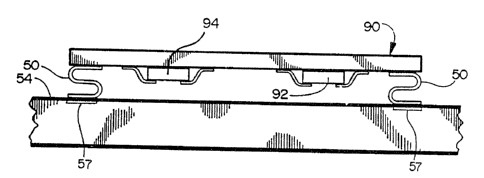
FIG. 5B illustrates the compliant connection
WO 93/07657 ~ ~ ~ 5 ~ ~ P~ P~'if'/US92/08320
-11-
formed by leads 50 between a multiple-chip module (MCM)
90, with integrated circuit chips 92 and 94. mounted on
,_
MCM 90, and circuit board 54. A multiple~chip module is
a cost effective packaging technology which integrates
a high input/output count with complex integrated
circuits and associated passive devices in close
proximity on a dense interconnect substrate . An MCM may
typically be capable of operating speeds up to the
gigahertz range using several relatively diverse
approaches to provide a system level capability. MCM 90
is typically a ceramic substrate which has metalized
circuit contacts electrically connected to chips 92 and
94. MCM 90 could also be an organic laminate. MCM 90
is mounted to circuit board 54 with leads 50 of the
present inventa.on. The same self-centering action
between chip carrier 52 and leads 50 described with
reference to FIG. 5A also occurs with MCM 90. In other
words, the surface tension of the solder causes MCM 90
and Leads 50 to self-center relative to the solder
joints between leads 50 and contacts on MCM 90. In
addition, self-centering also occurs at the solder
joints between leads 50 and 'the circuit contacts on
circuit board 54.
Chips 92 and 94 can be connected to MCM 90 by
any suitable means including wire bonding or soldering.
If chips 92 and 94 are'soldered to MCM 90, MCM 90 is
preferably connected, via leads 50, to circuit board 54
in a particular manner. First, chips 92 and 94 are
soldered to MCM 90. Then, leads 50 are connected to MCM
90 by reflowing the solder on leads 50. The leads 50,
attached to MCM 90, are placed in alignment with the
mounting pads on circuit board 54. In other words, MCM
90 is positioned to rest against leads 50 which are, in
turn, resting against the circuit contacts on circuit
WO 93/07657 PCT/US92/08320
211~5~3
-~2-
board 54. Then, the entire assembly is put through the
vapor phase soldering process. The colder at the '
junctions between leads 50 and MC~I 90, and the junctions
between leads 50 and circuit board 54 flow so that the
leads come into alignment with the circuit contacts on
MCM 90 and the board contacts on circuit board 54. This
has proven to be a cost effective manner in attaching
chips to board 54.
FIG. fl shows a second embodiment of the curved
lead of the present invention. Lead 70 includes a
single piece of conductive material having a first
portion 72 for connection to the chip carrier. Lead 70
also includes a second portion 74 for connection to the
circuit board. Portions 72 and 74 are coupled by a
curved portion 76. Thus, lead 70 is a generally C-
shaped lead and has a lower profile than the S-shaped
lead 50. As with lead 50, lead 70 is solder plated with
adequate solder plating 77 to form solder joints with a
chip carrier and a circuit board. Lead 70 is also
coupled to a support strip 79 and optionally scored for
ease of disconnection from strip 79.
FIG. 7 shows a third embodiment of a lead of
the present invention. Lead 80 is formed of a single
piece of conductive material having a first leg 82 for
connection to a leadless chip carrier and a second leg
84 for connection to a~circuit board. Legs 82 and 84
are connected by a generally diagonal portion 8C and two
curved portions 83 and 85. Thus, lead 80 is a generally
Z-shaped lead. As with leads 50 and '70, lead 80 is
solder plated with solder plating 87. Lead 80 is also ,
coupled to a support strip 89 and optionally scored for
ease of disconnection from strip 8s.
It is essential that the plated leads 50, 70
and 80 of the present invention have adequate solder
WO 93/07657 2 ~ 1 ~ ~ ~C ~ P(.'T/US92/08320
-13-
plating to form reliable solder joints. For example,
0.3 mils of solder plating is an inadequate amount of
solder to form a reliable joint for 50 mil components.
A range of solder plating having a thickness of 0.3 mils
to 1.5 mils is preferred depending on the pitch (i.e.,
mil - 50 mil). It has been observed that 1.0 to 1.1
mil solder plating on the plated leads of the present
invention provides excellent solder joint formation for
50 mil components.
10 It is preferred, although not required, that
the solder plating be a tin/lead solder having a
eutectic mixture. One preferred mixture is 63% Sn and
3a% pb ~ 5%.
In addition, the leads must be formed to a
15 dimension which allows adequate clearance for the solder
plating. In other words, by example, for a 50 mil
standard spacing, the leads of the present invention are
preferably formed with an 18 mil thickness dimension.
The 1 mil solder plating is then added.
Also, it is preferred that the single piece of
conductive material used to form the leads of the
present invention be formed to its final shape before
being plated. For example, it is preferred that
conductive portion 56 of lead 50 be formed in an S-shape
before it is plated with solder plating 62. The reason
for forming the conductive material prior to plating is
that, if conductive portion 56 were plated first and
then formed, cracks in the solder plating would tend to
form in the curved portions of the lead. These cracks
can cause solderability problems and solder joint
formation problems. I3owever, when the conductive
portions are formed to substantially their final shape,
and then plated, the solder plating is essentially
uniform along the entire surface of the conductive
WO 93/07657 FCT/U592/0~320
2115~~3
portion 56 of the lead.
The plated leads of the present invention '
provide substantial advantages over leads~of the prior
art which used solder beads. First, the cost of the
leads of the present invention is low in comparison to
the cost of the leads using solder beads. The beads do
not need to be assembled on the leads. Thus, one entire
step of assembly is eliminated. Absence of the solder
beads and tangs also means that the leads of the present
invention can be spaced closer together. Thus, lead
density is increased. The plated leads of the present
invention also take advantage of a capillary effect
during th' soldering process. This substantially
reduces the amount of solder running away from the
desired solder joints. Thus, the compliancy of the
leads is maintained and the number of solder bridges and
short circuits is drastically reduced. In addition,
signal quality degradation caused by solder running out
of the desired solder joint is drastically reduced.
Finally, the plated leads of the present invention are
plated after they are formed. Therefore, the plating is
uniform throughout the length of the plated lead.
Although the present invention has been
described with reference to preferred embodiments,
workers skilled in the art will recognise that changes
may be made in form and'detail without departing from
'the spirit and scope of the invention.
a. . .. ... . ,, ,...~. ,., ,