Note: Descriptions are shown in the official language in which they were submitted.
2t 1~8~8
BATTERY PACK INCLUDING STATIC MEMORY AND
A TIMER FOR CHARGE MANAGEMENT
The present invention relates to a battery pack
for a computer system including static memory to retain
battery operating parameters and charge information and
a real time clock for measuring periods of non-use.
2.
Computers are often needed in locations where AC
power is not available. Re~rgeable batteries are
typically used as an alternative source of power, such
as nickel-based batteries including nickel cadmium
(NiCad) and nickel metal hydride (NiMH) batteries,
which are capable of providing power to a portable or
pen-based computer for several hours. Since
rechargeable batteries have a limited cycle life, it is
desirable to maximize the life of and to obtain the
maximum power from each battery during every discharge
cycle. To achieve these goals, it is necessary to
fully and efficiently charge the battery without
causing temperature abuse as a result of overcharging.
Many battery chargers presently in use do not
efficiently charge a rechargeable battery, thereby
limiting the useful life of the,battery. The total
charge capacity of a battery, typically referred to as
the amp-hour (Ah) rating or otherwise called the milli-
amp-hour rating (mAh), tends to change over time and
usage. For example, the charge of a battery typically
increases and then decreases over time and usage until
the battery eventually will not hold a charge and must
2 1 1 8 8 ~ ~
be replaced. In particular, NiCad batteries exhibit a memory
effect causing lower capacity after multiple partial charge and
discharge cycles have occurred. Some battery chargers monitor
the temperature and voltage to avoid fast charging when the
battery voltage is too low or when the battery temperature is not
within an acceptable fast charging temperature range. Examples
are disclosed in Canadian patent application File No. 2,052,353
filed September 27, 1991 and U.S. patent No. 5,382,893. These
and most other known battery chargers do not have the capability
to accurately determine the charge level and the total charge
capacity and thus may still overcharge the battery, thereby
further reducing its useful life.
The primary reason for temperature abuse and overcharging of
nickel-based batteries was the difficulty of determining the
charge level since the voltage is substantially the same
regardless of the charge level. Furthermore, if the battery was
removed and then later re-installed, the system had no way of
determining the charge history and the remaining charge level of
the battery. Some methods estimated the charge level by
monitoring the charge and discharge current through the battery
over a period of time, but these methods still assumed an initial
level of charge. These methods proved inaccurate when a
partially discharged battery was used. Although the level of
discharge may be measured for a single dedicated battery in a
particular system, the battery is typically interchangeable with
another in many systems, so that the system has no way of
determining the charge level of a given battery. Also,
rechargeable batteries tend to discharge during periods of non-
use, referred to as self-discharge, so that a system which was
shut off for a period of time and then powered up could not
.~ J
21 1881~
determine the amount of self-discharge that had occurred.
One particular technique used in personal computers, known
as "Battery Watch", estimates the amount of charge remaining
based on the lapsed time of charge and discharge and converts
this to the useful time remaining. This technique has proven
unreliable since it assumes that the total charge capacity of a
battery does not change over time. Further, this technique fails
to keep track of the charge-in and charge-out and does not
account for the self-discharge.
One approach to solve most of these problems is disclosed in
Canadian patent application File No. 2,106,672 entitled "Battery
Charge Monitor and Fuel Gauge" filed January 20, 1993. A battery
pack was disclosed which included a nickel-based battery, a
microcontroller circuit and memory. Since the microcontroller
circuitry was contained within the battery pack, it was capable
of monitoring the battery charge status at all times by
continually sampling the charge and discharge current through the
battery as well as the battery voltage and temperature while
charging. The microcontroller used the battery charge status
information to accurately calculate the total charge capacity and
the remaining charge level in the battery. The memory stored the
charge information and a communication means was provided to
transfer the stored information to a computer system when the
battery pack was installed in the computer.
The advantages of this system include the ability to
recalculate the total capacity of the battery over time,
to provide a fuel gauge to continually measure the
remaining charge level of the battery at any given
time and the ability to measure the battery self-
discharge during periods of non-use. The local battery
~1 1 8~1 ~
circuitry also controlled battery charging and used the
above calculations to determine the optimal point of
fast charge termination for the battery. Essentially,
all charging functions and control were provided in the
battery pack, alleviating the need for the computer
system to determine when a new battery was placed into
the system and how to charge the battery.
It has been discovered that the use of
microcontroller circuitry in the battery pack is
relatively expensive and also reduces battery
shelf-life since the microcontroller circuit
continuously draws a significant amount of current from
the battery during periods of non-use. The power
consumption is particularly relevant when the size and
charge capacity of the nickel-based battery itself is
reduced for purposes of convenience and cost. The
microcontroller circuitry consumes valuable space and
adds cost since it must be purchased with each battery
pack. Computer designers must seek new ways to
maximize power consumption efficiency and valuable
space to meet the needs of the computer market. This
is particularly pertinent with the advent of pen-based
computer systems where size, cost and power usage are
critical.
It is desirable, therefore, to keep track of the
particular battery statistics and charge status,
including total capacity over time as well as the
instantaneous charge level at any given time, taking
into account periods of self-discharge and reduced
capacity. It is further desirable maximize the useful
power of the battery while keeping the size of the
battery as small as possible.
2 1 ~ 8~ 1 8
The invention in one aspect provides a removable battery
pack for providing power to a computer system, the computer
system including a microcontroller for detecting when the battery
pack is connected to the computer system, means coupled to the
microcontroller for determining the amount of charge provided to
and provided by the battery pack while the battery pack is
connected and computer system communication means coupled to the
microcontroller for communicating with the battery pack. The
battery pack comprises a rechargeable battery, a real time clock
coupled to the battery for continually providing an indication of
the present time and memory coupled to the battery for storing a
timestamp value of the present time indication and a numerator
value representing the remaining charge of the battery at
approximately the time indicated by the timestamp value. Thus
the microcontroller detects the battery pack when it is initially
connected to the computer system, retrieves the present time
indication and the timestamp and numerator values and thereafter
periodically updates the numerator based on the amount of charge
provided to and provided by the battery and also updates the
timestamp value with the present time indication while the
battery pack is connected to the computer system.
Another aspect of the invention pertains to a computer
system, comprising a removable battery pack, comprising a
rechargeable battery, a real time clock coupled to the battery
for continually providing an indication of the present time and
memory coupled to the battery for storing a timestamp of the
present time indication and a numerator representing the
remaining charge of the battery at approximately the time
indicated by the timestamp. Battery pack communication means is
coupled to the battery, the real time clock and the memory for
receiving, storing and transmitting the present time indication,
the timestamp and the numerator. There is a host computer for
coupling to and receiving power from the battery pack, the host
computer comprising means for coupling to the battery pack for
measuring the amount of charge provided to and provided by the
battery and host computer communication means for coupling to the
battery pack communication means for interfacing the host
5A 2 1 1 8 8 1 8
computer with the real time clock and the memory of the battery
pack. Means is provided for detecting installation of the
battery pack to the host computer and processing means is coupled
to the host computer communication means, the detecting means and
the measuring means, wherein the processing means retrieves the
timestamp, the numerator and the present time indication after
the detecting means detects installation of the battery pack and
thereafter, while the battery pack is connected to the host
computer, the processing means periodically updates the numerator
based on the amount of charge provided to and provided by the
battery and also periodically updates the timestamp with the
current value of the present time indication.
Still further the invention pertains to a method for
determining the elapsed time, during which a battery in a
removable battery pack of a computer system is self-discharging,
wherein the battery pack includes memory, comprising the steps of
the battery pack continually providing a present time value,
detecting whether the battery pack is installed on the computer
system while the computer system is powered on, when the battery
pack is first detected installed on the computer system,
retrieving the present time value and a timestamp of the present
time value previously stored in the memory of the battery pack,
subtracting the retrieved stored timestamp from the present time
value to calculate the elapsed time and periodically reading a
new timestamp of the present time value and storing the new
timestamp in the battery pack memory while the battery pack is
connected to the computer system and while the computer system
is powered on.
Further still, the invention comprehends a method for
determining the amount of self-discharge of a battery in a
removable battery pack of a computer system wherein the battery
pack includes memory, comprising the steps of the battery pack
continually providing a present time value, detecting whether
the battery pack is installed on the computer system while the
computer system is powered on, monitoring the amount of charge
added to the battery during charging and the amount of charge
removed during discharging of the battery while the battery pack
is detected installed on the computer system, retrieving the
present time value and a previously stored timestamp of the
21 t8818
5B
present time value from the battery pack memory when the battery
pack is first detected installed on the computer system,
subtracting the retrieved stored timestamp from the present time
value to calculate an elapsed time of self-discharge,
calculating the amount of self-discharge by multiplying the
elapsed time by a predetermined self-discharge rate and
periodically reading a new timestamp of the present time value
and storing the new timestamp into the battery pack memory while
the battery pack is detected installed.
More particularly, a battery charge monitoring system
according to the present invention includes a battery pack which
further includes a battery, a timer and static memory to keep
track of the operating parameters and charge status of the
battery at all times and communication means to report the
battery information. A microcontroller is provided in the DC-DC
converter of the computer system to retrieve and update battery
information from the battery pack, to control charging functions
of the battery, to report charge status and information of the
battery to the host computer and also to perform other
housekeeping functions of the DC-DC converter. The housekeeping
functions include auxiliary battery detection and operation, low
battery voltage detection and operations, power and standby
detection and control and communication with the host computer.
The static memory within the battery pack preferably includes a
read only memory (ROM) and a random access memory (RAM). A
communication link is also provided in the battery pack to
communicate with the microcontroller, where the communication
link is preferably implemented as a single line or one-wire
serial link to reduce the number of battery pack terminals.
In the preferred embodiment, the operating parameters
stored in the ROM memory of the battery pack includes a family
code and battery type, maximum charge temperature, low voltage
set points, initial rated total capacity and self-discharge
rates for several time periods. The timer is preferably a real
time clock (RTC) preferably in the form of a binary counter
measuring elapsed time in seconds and providing an
indication of the present time. The microcontroller
regularly retrieves and stores a timestamp value from
the RTC and stores the timestamp back into the RAM in
21 1 ~81 ~
the battery pack, so that when the battery is removed,
the stored timestamp indicates the time the battery
pack was removed. The RAM also stores two fuel gauge
values including a numerator representing the remaining
charge on the battery and a denominator representing an
updated version of the total capacity of the battery.
The microcontroller in the DC-DC converter detects
power up or new battery pack installation in the system
and retrieves the stored data, so that the
microcontroller can determine the charge startup and
operating conditions of the battery. The numerator and
denominator values are read and checked for validity to
determine the remaining and total charge capacities.
The RTC present time value is read and compared to the
timestamp value to determine elapsed time indicating
the amount of self-discharge. The self-discharge rates
are read and the time of self-discharge is converted to
lost charge using the self-discharge rates and
subtracted from the retrieved numerator to update the
numerator. A new timestamp value and numerator are
stored to update the battery pack, and these values are
updated regularly during operation. Note that the
numerator indicates the level of charge at the time of
the timestamp. The denominator value in the battery
pack is also updated after a full charge and discharge
cycle occurs so that a good approximation of the total
capacity of the battery is maintained. The
microcontroller also includes one or more communication
lines to provide the battery status and statistics to
the host computer on a periodic basis or when
requested.
Since the microcontroller circuitry is moved to
the DC-DC converter from the battery pack and since the
battery pack includes the static memory and a timer,
all the advantages of maintaining battery parameters
2 1 1 88 1 ~
and tracking battery charge status are achieved while
also reducing the size and cost of the battery pack and
increasing the battery pack shelf-life. In the
preferred embodiment, the static memory comprising RAM
and ROM, the RTC and the communication circuitry are
all provided on a single chip. Furthermore, the
battery pack includes circuitry to use power from the
AC adapter when available to prevent the RAM/RTC from
draining power from the battery, which maximizes the
life of the battery.
The DC-DC controller further includes a convenient
and cost effective method to trickle charge the battery
upon completion of fast charge. To implement fast
charging, a transistor switch, preferably comprising an
N-channel metal oxide semiconductor field effect
transistor (MOSFET), is placed in the charge path of
the battery and controlled by the microcontroller. The
microcontroller turns on the transistor switch to allow
the AC adapter to fast charge the battery. A trickle
or top off charge is then applied to the battery for a
period of time after fast charging is completed to
increase the useful life of the battery. In the
preferred embodiment, the microcontroller controls the
pulse trickle charge by pulsing the MOSFET on and off
for approximately 2 hours, where the pulse signal has a
period preferably between 1-2 seconds and duty cycle of
approximately 5-10%. The pulse charging technique
simulates trickle charge since the average amount of
current during pulse charging is roughly equivalent to
the steady state trickle charge current level typically
used. The MOSFET is then turned off and a resistor in
parallel with the MOSFET allows a maintenance charge to
flow through the battery to maintain its charge level.
In this manner, the microcontroller simulates trickle
charging, which would otherwise require extra trickle
2 1 1 88 1 8
charge and sophisticated current measuring circuitry,
such as the current regular and measuring circuits
described in U.S. Patent No. 5,136,231 entitled "Ni-Cad
Battery Charge Rate Controller."
The microcontroller is capable of being placed in
standby mode to reduce power consumption when the
computer system is not being used for a period of time.
A standby switch operated by the user of the computer
system is also provided which was typically monitored
lo by the keyboard controller. Since the keyboard
controller had to remain powered-up to monitor the
standby switch, and since the keyboard controller draws
a significant amount of power, the computer system
still consumed a significant amount of power while in
standby. One solution was to provide a special ASIC to
monitor the standby switch to allow the keyboard
controller to shut down. This solution, however, is
expensive. In the preferred embodiment of the present
invention, the microcontroller in the DC-DC converter
monitors the standby switch and controls standby mode
to allow the keyboard controller to be shut down and to
eliminate the need for special monitoring circuitry or
an ASIC.
A better understanding of the present invention
can be obtained when the following detailed description
of the preferred embodiment is considered in
conjunction with the following drawings, in which:
Figure 1 is a schematic block diagram of a
computer system using a charge management battery pack
according to the present invention;
Figure 2 is a schematic diagram of the battery
pack of Figure 1;
Figure 3 is a block diagram showing the alignment
of the block and schematic diagram of Figures 3A-3C;
21 l~sla
Figures 3A-3C are schematic and block diagrams Of
the DC-DC controller of Figure 1;
Figures 4A-4H are flowchart diagrams illustrating
the operation of firmware executed by the
microcontroller of Figure 3;
Figure 5 is a flowchart diagram illustrating an
external power and standby switch routine operating on
the microcontroller of Figure 3;
Figure 6 is a flowchart diagram illustrating an
update RAM/RTC routine executed by the microcontroller
of Figure 3; and
Figure 7 is a flowchart diagram illustrating a
host serial receive routine executed by the
microcontroller of Figure 3.
- -
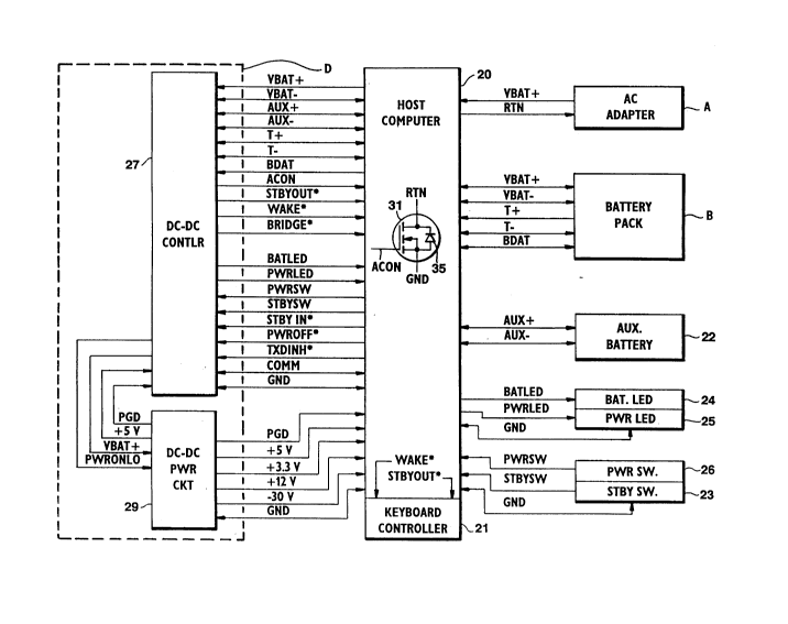
Referring now to Figure 1, a computer system C is
shown which uses a charge management battery pack B
according to the present invention. The computer
system C includes a host computer 20 which preferably
includes a DC-DC converter D. The computer system C is
preferably configured to receive the removably
connected battery pack B, a removably connected
auxiliary battery 22 and a removably connected AC
adapter A. Although shown separately, the DC-DC
converter D is preferably a subsystem of and contained
within the host computer 20. Two light emitting diodes
(LEDs) are provided and connected to the host computer
20, including a battery LED 24 activated by a signal
BATLED and a power LED 25 activated by a signal PWRLED.
These signals are referenced to a signal GND, otherwise
referred to as ground. A momentary power switch 26 and
a momentary standby switch 23 each provide a low pulse
on a PWRSW signal and a STBYSW signal, respectively, to
the host computer 20 when the corresponding switch is
pressed by the user of the computer system C. The
2 1 1 38 1 ~
power switch 26 toggles the computer system C on and
off upon consecutive presses, whereas the standby
switch 23 is used to place the computer system C in or
out of standby mode upon consecutive presses.
The AC adapter A converts AC voltage from an AC
- line to a generally unregulated DC voltage ranging
between 10 and 18 volts between a signal VBAT+ and a
signal RTN. The AC adapter A preferably does not
include a power switch, but is considered powered on
when connected to the AC line and to the host computer
20, and considered powered off otherwise. When the AC
adapter A is present and powered on, it provides the
main power source for the computer system C and also to
charge a rechargeable battery 28 (Fig. 2) within the
battery pack B. The battery 28 provides power to the
computer system C when the AC adapter A is powered off.
The battery 28 is preferably a 10 cell nickel-based
battery, such as a nickel cadmium (NiCad) or a nickel-
metal hydride (NiMH) battery, where each cell
preferably has a nominal voltage of 1.2 volts. Thus,
the battery 28 preferably provides a nominal voltage of
approximately 12 volts, although its voltage may vary
significantly depending upon its charging condition and
remaining charge level. In any event, the voltage
across the battery 28 should not exceed 17 volts.
The battery 28 preferably has a nominal capacity
of approximately 2.2 amp-hours (Ah), where the Ah
capacity generally defines the full charge capacity of
a rechargeable battery, although the charge capacity
typically changes over time and usage. In practice,
the original Ah capacity rating is derived from the
battery cell manufacturer's specification sheet, by
calculating the total number of coulombs provided by
discharging a fully charged battery cell until its
voltage becomes equal to a discharge voltage level,
~l lQ~1~3
which is preferably 1.0 volts for each cell, or
approximately 10 volts for the battery 28. Since the
total capacity of the battery 28 changes over time and
usage, a measure of the full charged capacity,
otherwise referred to as the denominator, is
recalibrated and stored after a full charge cycle,
described below, to keep track of the changing full
charge capacity of the battery 28 over time. The
remaining charge level of the battery 28, otherwise
referred to as the numerator, is regularly monitored
and updated.
An N-channel metal oxide semiconductor field
effect transistor (MOSFET), referred to as the AC
MOSFET 31, is preferably located within the host
computer C and has its drain coupled to the RTN signal,
its source coupled to the GND signal and its gate
receiving a signal referred to as ACON. An inherent
diode 35 is provided within the AC MOSFET 31 having its
anode connected to the source and its cathode connected
to the drain of the AC MOSFET 31. Even if the AC
MOSFET 31 is off, its diode 35 is forward biased when
the AC adapter A is powered on, allowing the AC adapter
A to provide power to the computer system C. As will
be described below, the DC-DC converter D detects the
presence of the AC adapter A and asserts the ACON
signal high, which activates or turns on the AC MOSFET
31, bypassing its inherent diode 35. The AC MOSFET 31
is provided to prevent discharging of the battery 28
when the AC adapter A is connected to the host computer
20 but powered off.
The battery 28 of the battery pack B has its
positive terminal coupled to the VBAT+ signal when
installed in the computer C, and its negative terminal
providing a signal VBAT-. The battery pack B also
includes a temperature sensor TS connected between
21 1~
signals T+ and T- for providing a signal indicative of
the temperature of the battery 28. When the battery
pack B is installed, the T- signal is connected to
ground. A signal BDAT allows a one-wire serial
communication port between the battery pack B and the
DC-DC converter D, as will be further described below.
The auxiliary battery 22 provides a voltage range
of preferably approximately 6-8 volts between signals
AUX+ and AUX-, and preferably has a capacity of 50 mAh.
The auxiliary battery 22 is used to provide power to
the computer system C while changing the battery pack B
with a similar battery pack. As will be described in
more detail below, the computer system C must be in a
standby mode before the auxiliary battery 22 provides
power, since the auxiliary battery 22 is capable of
sustaining a fully loaded computer system C for only
approximately 1 minute in standby mode to facilitate
replacement of the battery pack B.
The DC-DC converter D includes a DC-DC controller
27 and a DC-DC power circuit 29, both of which are
connected to the host computer 20. The DC-DC
controller 27 is connected to the VBAT+, VBAT-, AUX+,
AUX-, T+, T-, PWRSW, STBYSW and BDAT signals as well as
GND. The PWRSW signal is debounced by the DC-DC
controller 27, where the DC-DC controller 27 asserts a
signal PWRONLO in response to activate the DC-DC power
circuit 29. The DC-DC power circuit 29 is then
activated, providing power signals +5V, +3.3V, +12V and
-30V having regulated voltage levels of approximately 5
volts, 3.3 volts, 12 volts and -30 volts, respectively,
to the host computer 20.
The DC-DC power circuit 29 is preferably a buck-
type pulse width modulated DC-DC converter operating in
the flyback mode. It converts an unregulated DC
voltage from either the battery 28 or the AC adapter A
21 1 8~
into the regulated voltages listed above. The DC-DC
power circuit 29 includes a power-on delay and
comparator circuit (not shown), which is initiated upon
receipt of the PWRONLO signal. The delay circuit
asserts a power good signal PGD to the DC-DC controller
27 and to the host computer 20 upon expiration of the
delay if the +5V, +3.3V, +12V and -30V power signals
are all within proper tolerance levels. The VBAT+
signal is provided to the DC-DC power circuit 29 from
the DC-DC controller 27, and the DC-DC power circuit 29
provides the +5V signal to the DC-DC controller 27.
The DC-DC controller 27 receives and debounces the
STBYSW signal. In response to receiving a low pulse on
the STBYSW signal, the DC-DC controller 27 asserts a
signal STBYOUT* low to a keyboard controller 21 within
the host computer 20 to initiate the standby mode. An
asterisk at the end of a signal name denotes negative
logic, where the signal is asserted low and negated
high unless otherwise stated. The host computer 20
responds to receiving the STBYOUT* signal asserted low
by asserting a signal STBYIN* low to the DC-DC
controller 27 to initiate standby mode. The keyboard
controller 21 enters into an internal power down mode
during standby to conserve energy. The DC-DC
controller 27 also enters into a low power mode during
standby, although it is awakened on a periodic basis.
The DC-DC controller 27 includes a microcontroller
72 (Fig. 3B), which is preferably programmed to bring
the computer system C out of standby mode using a
signal referred to as WAKE*. The keyboard controller
21 receives the WAKE* signal to execute required
functions during standby. Other devices, such as an
external modem (not shown), may wake up the computer
system C or pull it out of standby mode. This is not
desired, however, if the computer system C is being
- 21 1 ~81 8
powered solely by the auxiliary battery 22 since it may
drain too quickly preventing reliable operation. A
signal BRIDGE* is asserted low by the DC-DC controller
27 to prevent wakeup in this case. The host computer
20 may be programmed to shut down by asserting a signal
PWROFF* to the DC-DC controller 27 to initiate power
down operations.
The DC-DC converter D communicates to the host
computer 20 through a serial communication signal
referred to as COMM. The DC-DC converter D broadcasts
information to the host computer 20 on the COMM signal
unless the host computer 20 asserts a signal TXDINH*
low. When the TXDINH* signal is asserted low by the
host computer 20, it can transmit data to the DC-DC
converter D on the COMM signal.
The DC-DC controller 27 constantly monitors the
functions of the computer system C to determine the
mode and whether power is being provided by the AC
adapter A, the battery pack B or the auxiliary battery
22. The DC-DC controller 27 allows normal operation as
long as the VBAT+ signal rises above a predetermined
minimum voltage level, which is preferably
approximately 10 volts. If the VBAT+ signal falls
below this minimum voltage level during normal
operation, the DC-DC controller 27 shuts down the
computer system C.
The battery LED 24 generally indicates the charge
and voltage status of the battery 28. If the battery
28 is being fast charged, then the BATLED signal is
asserted continuously so that the battery LED 24
remains on. During operation using the battery 28
alone, if the voltage of the battery 28 falls below a
predetermined first voltage level or set point,
referred to as LOWBAT1, the DC-DC controller 27 informs
the host computer 20 through communication on the COMM
2i 18818
signal, and preferably asserts a 1 Hertz (Hz) signal on
the BATLED signal so that the battery LED 24 blinks at
a 1 Hz rate. The LOWBAT1 set point voltage is
preferably approximately 11.5 volts. The host computer
20 also beeps to inform the user. If the computer
system C is in standby mode, a slightly higher set
point voltage is used, referred to as SLOWBAT1, which
is preferably approximately 11.7 volts.
If the voltage of the battery falls below a
second, lower predetermined voltage set point, referred
to as LOWBAT2, the DC-DC controller 27 informs the host
computer 20 in a similar manner and preferably asserts
a 2 Hz signal on the BATLED signal so that the battery
LED 24 blinks at a 2 Hz rate. The LOWBAT2 voltage set
point is preferably approximately 11.2 volts unless in
standby, where a slightly higher voltage set point,
referred to as SLOWBAT2, is used which is preferably
approximately 11.4 volts. Again, the host computer 20
informs the user with a beep. Note that the standby
set points are both 200 mV higher than the
corresponding regular set points.
The user may replace the battery pack B with a
fresh battery pack when the computer system C is
operating by first pressing the standby switch 23 to
place the computer system C in standby, and then
removing the discharged battery pack B. The user
preferably has at least one minute, during which time
the auxiliary battery 22 provides power to the computer
system C while in standby. After a new battery pack is
installed, the user presses the standby switch 23 to
pull the computer system C out of standby mode. If the
user fails to replace the battery pack B with a fresh
pack, or otherwise does not connect the AC adapter A,
the DC-DC controller 27 shuts down the computer system
21 18818
16
C if the VBAT+ signal falls below the minimum voltage
level of 10 volts.
Referring now to Figure 2, a schematic diagram of
the battery pack B is shown which includes charge
management circuitry according to the present
invention. The terminals of the battery pack B are
shown collectively as terminals 30 and labeled with the
corresponding signal names. The temperature sensor TS
is preferably a thermistor coupled in good thermal
contact with the battery 28 having a nominal resistance
of approximately 10 kn at a temperature of 25 degrees
Celsius (C), and having a negative temperature
coefficient so that its resistance changes
proportionately with its temperature. The circuit
connected to the temperature sensor TS and used to
measure the temperature of the battery 28 is described
more fully below.
The VBAT+ signal is connected to one side of a
resistor 32 and to the collector of an NPN transistor
36. The other side of the resistor 32 is connected to
the cathode of a Zener diode 34 and to the base of the
transistor 36. The Zener diode 34 preferably has a
reverse breakdown voltage of 5.6 volts and the
transistor 36 is preferably a 2222-type transistor.
The anode of the Zener diode 34 is connected to a local
battery ground, referred to as BGND, which is also
connected to the anode of another Zener diode 38. The
Zener diode 38 preferably has a reverse breakdown
voltage of 5.1 volts, and has its cathode connected to
the emitter of the transistor 36. The Zener diode 38
provides surge protection for the RAM/RTC 40. A filter
capacitor 42 is coupled between the emitter of the
transistor 36 and BGND. The resistor 32, the Zener
diode 34 and the transistor 36 serve as an emitter
follower regulator 39 coupled between the VBAT+ and
2 1 ~
BGND signals to provide a relatively constant 5 volts
at the emitter of the transistor 36.
The BGND signal is connected to the GND, CLK, VCC,
and VBATB pins of a DS1608 EconoRAM Time Chip, referred
to as the RAM/RTC 40, which is manufactured by Dallas
~ Semiconductor. The DSl608 is preferably used since it
conveniently includes an internal static RAM and a ROM
for storing the operating parameters and charge status
information of the battery 28, a real time clock (RTC)
for measuring periods of non-use of the battery 28, and
a 1-wire serial communication capability for exchanging
information of the battery 28 with the DC-DC converter
D. Other similar type of devices performing similar
functions could be used, such as the DS2404 also
manufactured by Dallas Semiconductor, or an ASIC
incorporating the described functions, to name a couple
of examples.
The emitter of the transistor 36 is connected to a
VBATO pin of the RAM/RTC 40. A crystal oscillator 44
is connected between the X1 and X2 pins of the RAM/RTC
40, where the crystal 44 preferably has an oscillating
frequency of approximately 32.768 kHz and an inherent
capacitance of 6 pF. It is noted that if the VBATO pin
is used to provide power to the RAM/RTC 40, then the
VCC and VBATB pins must be grounded for proper
operation.
A diode 46 has its anode connected to the BGND
signal and its cathode connected to an input/output
(I/O) pin of the RAM/RTC 40. The I/O pin is also
connected to the anode of a diode 48 and to one side of
a resistor 50, where the cathode of the diode 48 is
connected to the VBATO pin. The other side of the
resistor 50 provides the BDAT signal. The diodes 46
and 48 protect the RAM/RTC 40 from overvoltage swings
of the BDAT signal. The I/O pin of the RAM/RTC 40
21 13818
provides the one-wire serial communication port for
transferring serial data to and from the RAM and ROM
portions of the RAM/RTC 40. The details of this serial
communication is fully documented in the specification
sheets by the manufacturer and will not be described.
The data stored in the RAM/RTC 40 will be described
more fully below.
The BGND signal is connected to the anode of a
Schottky diode 52 having its cathode connected to the
VBAT- signal. A filter capacitor 54 is also coupled
between the BGND and VBAT- signals. Another Schottky
diode 56 has its cathode connected to the T- signal and
its anode connected to one side of a current limit
resistor 58, where the other side of the resistor 58 is
connected to the BGND signal. The resistor 58
essentially limits excessive charge current through the
Schottky diode 56 when the battery 28 is initially
installed and the VBAT- signal is momentarily connected
before the T- signal. The Schottky diodes 52 and 56
operate in conjunction with the emitter follower
regulator 39 to provide a relatively constant 5 volts
to the RAM/RTC 40 regardless of whether power is being
provided by the battery 28 or the AC adapter A. When
the battery pack B is not installed, the T- signal is
left floating so that the Schottky diode 56 is biased
off and the VBAT- signal provides a ground through the
Schottky diode 52. If the battery pack B is installed,
the T- signal is connected to system GND. However, if
the AC adapter A is not connected or is not powered on,
the Schottky diode 56 is still biased off and the
Schottky diode 52 is biased on.
When battery pack B is installed and the AC
adapter A is also installed and powered on, the AC
adapter A attempts to pull the voltage between the
VBAT+ and GND signals to 18 volts, so that the voltage
21 18818
19
across the VBAT+ and GND signals exceeds the voltage
across the battery 28 or across the VBAT+ and VBAT-
signals. Thus, the diode 52 is biased off and the
diode 56 is biased on, so that the T- signal provides a
reference ground for the battery pack B. In any the
case, the emitter follower regulator 39 maintains a
constant 5 volts to the RAM/RTC 40 whether powered by
the battery 28 or the AC adapter A, and the AC adapter
A powers the RAM/RTC 40 when available.
Referring now to Figures 3A-3C, a partial block
and schematic diagram is shown of the DC-DC controller
27. The VBAT+ signal is connected to one side of a
filter capacitor 60 and to the input pin of a precision
voltage regulator 62, which is preferably an LP2951
manufactured by National Semiconductor. The other side
of the capacitor 60 is coupled to ground. The output
pin of the voltage regulator 62 provides a relatively
accurate 5 volt reference signal referred to as +5VREF,
which is coupled to one side of a filter capacitor 64
and to its sense input pin. The other side of the
capacitor 64 is connected to ground. The voltage
regulator 62 has its 5VTAP and FB (feedback) pins
connected together. The +5VREF signal is provided to
the VDD input of the microcontroller 72, which is
preferably a TMP47C441 CMOS 4-bit microcontroller
manufactured by the Toshiba Corporation. The
microcontroller 72 includes an 8-bit analog to digital
(A/D) converter, a 4 kbyte ROM, a 128-byte RAM and
three internal timers, referred to as TIMER1, TIMER2
and the interval timer, respectively. The +5VREF
signal is also connected to an analog reference input
pin of the microcontroller 72 referred to as AREF,
establishing an analog reference input for the internal
A/D converter. The VASS and VSS pins of the
microcontroller 72 are connected to ground.
2 1 1 ~
The VBAT- signal is connected to the drain of an
N-channel MOSFET 74, to one side of a resistor 78 and
to one side of a resistor 80. The drain of the MOSFET
74 has several pins connected together to increase its
current capacity. The MOSFET 74 also includes an
inherent diode 76 having its anode connected to its
source and its cathode connected to its drain. The
gate of the MOSFET 74 receives a fast charge signal
referred to as FCFET, which signal is asserted high by
the microcontroller 72 to allow fast charging or
discharging of the battery 28. The resistor 78 has a
resistance to allow a maintenance charge through the
battery 28 when the battery 28 and the AC adapter A are
installed and the MOSFET 74 is turned off, where the
maintenance charge is preferably approximately 10 mA.
The other side of the resistor 80 is connected to
the anode of a diode 81, and the cathode of the diode
81 is connected to the I1 input of a battery voltage
measuring circuit 82. The battery measuring voltage
circuit 82 is connected to ground and has an output
providing a signal VBATT, which signal is connected to
one side of a diode 84 and to a first analog input pin
of the microcontroller 72, referred to as AN0. One of
the registers of the microcontroller 72 is defined to
implement four analog inputs, referred to as AN0, AN1,
AN2 and AN3, respectively, each of which are provided
to the internal 8-bit A/D converter depending upon
which one is desired to be measured. The cathode of
the diode 84 is connected to the +5VREF signal, where
the diode 84 protects the microcontroller 72 from
excessive voltage of the VBATT signal. The VBAT+
signal is connected to one side of a resistor 90 and to
the source of a P-channel MOSFET 86, which has its gate
connected to the other side of the resistor 90. The
drain of the MOSFET 86 is connected to one side of a
21 18818
resistor 88, which has its other side connected to the
I2 input of the battery voltage measuring circuit 82.
The gate of the MOSFET 86 is connected to the drain of
an N-channel MOSFET 92, which has its source connected
to ground and its gate connected to one side of a
resistor 94 and to a signal VCCON provided by a P22
output pin of the microcontroller 72. The other side
of the resistor 94 is connected to ground. A P21
output pin of the microcontroller 72 provides a signal
VRES, which signal is provided to the battery voltage
measuring circuit 82.
The battery voltage measuring circuit 82 operates
to measure the voltage levels of the VBAT+ and VBAT-
signals one at a time through the VBATT signal provided
to the microcontroller 72. The voltage across the
battery 28 may be calculated by sampling the VBAT+
signal and then the VBAT- signal and subtracting the
two values. The microcontroller 72 asserts the VCCON
signal high, which turns on the MOSFETs 92 and 86
providing the VBAT+ signal through the resistor 88 to
the battery voltage measuring circuit 82. Due to the
operation of the measuring circuit 82, the diode 81 is
reversed-biased so that the battery voltage measuring
circuit 82 provides an analog voltage at the VBATT
signal which is proportional to the VBAT+ signal. The
microcontroller 72 asserts the VRES signal high for low
resolution, where the VBAT+ signal may range from o to
20 volts. The VRES signal is asserted low by the
microcontroller 72 for higher resolution, where the
VBAT+ signal may range from 0 to 12 volts.
The microcontroller 72 asserts the VCCON signal
low to turn off the MOSFETs 92 and 86 and forward bias
the diode 81. In this manner, the VBAT- signal is
provided through the resistor 80 and the diode 81 to
the I1 input of the battery voltage measuring circuit
21 ~ssla
22
82, which asserts a proportional voltage at the VBATT
signal proportional to the VBAT- signal. The VRES
signal is asserted to implement low or high resolution
as described previously. The A/D converter of the
microcontroller 72 thus develops two 8-bit digital
numbers corresponding to the VBAT+ and VBAT- signals.
The source of the MOSFET 74 is connected to one
side of a sense resistor 96 and to the input of a
discharge current measuring circuit 98, where the other
side of the resistor 96 is connected to ground. The
discharge current measuring circuit 98 is also
connected to ground and samples the voltage across the
resistor g6, where this voltage has a level
proportional to the current through the battery 28.
The discharge current measuring circuit 98 has an
output coupled to one side of a resistor 100, which has
its other side connected to a signal DISCHARGE, so that
the DISCHARGE signal has a voltage level proportional
to the discharge current through the battery 28. The
DISCHARGE signal is provided to the AN1 analog input of
the microcontroller 72, so that the microcontroller 72
may sample the discharge current through the battery
28. The DISCHARGE signal is also connected to the
anode of a diode 102, which has its cathode connected
to the +5VREF signal. The diode 102 and the resistor
100 provide voltage and current protection for the
microcontroller 72 in case of an excessive voltage
level of the DISCHARGE signal.
The microcontroller 72 asserts a signal IRES at an
output pin P62, which is provided to one side of a
resistor 104 and to the discharge current measuring
circuit 98. The other side of the resistor 104 is
connected to ground and serves as a pulldown resistor.
The microcontroller 72 asserts the IRES signal high to
implement high resolution to measure the discharge
21 ! 8 a I ~
current through the battery 28, which may preferably
range between 0 and 460 mA. The microcontroller 72
asserts the IRES signal low for low resolution, where
the discharge current through the battery 28 may
preferably range from 0 to 3.677 amperes.
The source of the MOSFET 74 is connected to the Il
input of a charge current measuring circuit 108, which
has its I2 input pin connected to ground. The charge
current measuring circuit 108 provides an output to one
lo side of a resistor 112. The other side of the resistor
112 is connected to a signal CHARGE, which is also
connected to the anode of a diode 114 and to the AN2
input pin of the microcontroller 72. The cathode of
the diode 114 is connected to the +5VREF signal. The
diode 114 protects the microcontroller 72 from
excessive voltage levels of the CHARGE signal. The
charge current measuring circuit 108 measures the
voltage across the resistor 96 and asserts a voltage
signal at its output so that the CHARGE signal has a
voltage proportional to the amount of charging current
through the battery 28. The range of the charge
current measurements is preferably from 0 to 3.677
amperes. It is noted that while the details of the
discharge current measuring circuit 98 and the charge
current measuring circuit 108 are not shown, these
functions may be performed using circuits well known to
those skilled in the art of electronic circuit design.
Further, the currents measured are not used to control
a feedback loop as in typical when controlling the
trickle charge current through the battery 28.
The T+ signal is provided to one side of a pull-up
resistor 116, to one side of a filter capacitor 118 to
one side of a resistor 120, where the other side of the
resistor 116 is connected to the +5VREF signal, the
other side of the capacitor 118 is connected to ground
21 1~18
and the other side of the resistor 120 provides a
signal TEMP. The TEMP signal is connected to the anode
of a diode 122, to the cathode of a diode 124 and to
the AN3 analog input of the microcontroller 72. The
cathode of the diode 122 is connected to the +5VREF
signal and the anode of the diode 124 is connected to
ground. The T- signal is connected to ground when the
battery pack B is installed in the computer system C.
The resistance of the resistor 116 is preferably
approximately 20 kn to establish a voltage divider
comprising the resistor 116 and the temperature sensor
TS, so that the signal TEMP has a voltage proportional
to the temperature of the battery 28. The A/D
converter microcontroller 72 converts the voltage of
the TEMP signal to a digital number to measure the
temperature of the battery 28.
The microcontroller 72 includes an XIN pin and an
XOUT pin which are used for connecting to an external
oscillator circuit to establish a clock frequency for
the microcontroller 72. The XOUT pin is connected to
one side of a resistor 132, which has its other side
connected to one side of a capacitor 128 and to one
side of a crystal oscillator 130, which preferably has
a frequency of oscillation of approximately 2.45 MHz.
The XIN pin of the microcontroller 72 is connected to
the other side of the crystal 130 and to one side of
another capacitor 126, which has its other side
connected to ground. The other side of the capacitor
128 is also connected to ground. In this manner, the
oscillator 130, the resistor 132 and the capacitors 126
and 128 establish an operating frequency for the
microcontroller 72 of approximately 2.45 MHz.
The PGD signal is connected to a K02 input pin of
the microcontroller 72 and also to one side of a
resistor 134. The other side of the resistor 134 is
21 18818
connected to ground and serves as a pulldown resistor.
The PWROFF* signal is connected a K03 input pin of the
microcontroller 72 and to one side of a pulldown
resistor 136. The other side of the resistor 136 is
connected to ground. In this manner, the
microcontroller 72 detects the assertion of the PGD
signal and the negation of the PWROFF* signal, which
signals are otherwise pulled low.
The AUX+ signal is connected to the source of a P-
channel MOSFET 138 and to one side of a resistor 140,
which has its other side connected to the gate of the
MOSFET 138. The drain of the MOSFET 138 is connected
to the VBAT+ signal and its gate is connected to the
drain of an N-channel MOSFET 142, which has its source
connected to ground and its gate connected to one side
of a resistor 144 and to a signal AUXON. The other
side of the resistor 144 is connected to ground and the
AUXON signal is provided by the P20 pin of the
microcontroller 72. The MOSFET 138 includes an
internal diode 139 having its anode connected to the
drain and its cathode connected to the source of the
MOSFET 138, where the diode 139 allows the auxiliary
battery 22 to be charged even if the MOSFET 138 is off.
The MOSFET 138 serves as a discharge MOSFET for the
auxiliary battery 22, where the auxiliary battery 22
may only be discharged if the MOSFET 138 is turned on.
The resistor 144 serves to pull the AUXON signal low
thereby turning off the MOSFET 142 preventing
discharge. When the microcontroller asserts the AUXON
signal high, the MOSFET 142 is turned on, essentially
connecting the positive terminal of the auxiliary
battery 22 to the VBAT~ signal, thus allowing
discharge.
The AUX- signal is connected to one side of a
filter capacitor 146, to one side of a resistor 150 and
21 1881~
26
to the cathode of a Schottky diode 148. The other side
of the capacitor 146 and the anode of the diode 148 are
connected to ground and the other side of the resistor
150 is connected to the drain of an N-channel MOSFET
152. The source of the MOSFET 152 is connected to
ground and its gate is connected to an auxiliary charge
signal, referred to as AUXCHG, which is provided to the
P63 input pin of the microcontroller 72. The MOSFET
152 includes an internal diode 153 having its anode
connected to the drain and its cathode connected to the
source of the MOSFET 152, where the diode 153 allows
the auxiliary battery 22 to be discharged even if the
MOSFET 152 is turned off. The diode 148 also serves
this purpose but has a lower forward drop to conserve
energy. The MOSFET 152 serves as a charge MOSFET for
the auxiliary battery 22, so that the auxiliary battery
22 can only be charged when the MOSFET 152 is turned
on. The microcontroller 72 controls the MOSFET 152 by
negating the AUXCHG signal to turn the MOSFET 152 off
and by asserting the AUXCHG signal high to turn the
MOSFET 152 on.
The STBYIN* signal is connected to one side of a
pull-up resistor 154 and to the R90 input pin of the
microcontroller 72. The other side of the resistor 154
is connected to the +5VREF signal. The BDAT signal is
connected to one side of a resistor 156, which has its
other side connected to an R91 input pin of the
microcontroller 72, the anode of a diode 158, the
cathode of a diode 160 and one side of a pull-up
resistor 162. The cathode of the diode 158 and the
other side of the resistor 162 are connected to the
+5VREF signal, and the anode of the diode 160 is
connected to ground. The diodes 158 and 160 are
provided to prevent overvoltage swings of the BDAT
signal from harming the microcontroller 72. The
21 18818
_
TXDINH* signal is connected to an R92 input pin of the
microcontroller 72 and also to one side of a pull-up
resistor 164, which has its other side connected to the
+5VREF signal.
The microcontroller 72 includes an *RST pin, which
is connected to one side of a pull-up resistor 166, to
one side of a reset capacitor 170 and to the anode of a
diode 168. An asterisk preceding a device pin name
indicates that the device expects negative logic. The
other side of the resistor 166 is connected to the
+5VREF signal and the other side of the capacitor 170
is connected to ground. The cathode of the diode 168
is connected to an output pin *WTO of the
microcontroller 72. The resistor 166 normally pulls up
the *RST pin high, whereas assertion of the *RST pin
low resets the microcontroller 72. An internal
watchdog timer of the microcontroller 72 asserts the
*WTO output pin low upon timeout, which pulls the *RST
pin low through the diode 168 to reset the
microcontroller 72.
The PWRSW signal is connected to one side of a
resistor 172, which has its other side connected to one
side of a filter capacitor 176, to both inputs of a
two-input NOR gate 174 and to one side of a pull-up
resistor 178. The other side of the resistor 178 is
connected to the +5VREF signal and the other side of
the capacitor 176 is connected to ground. The output
of the NOR gate 174 provides a signal EXT PWR ON, which
is connected to one input of a two-input NOR gate 182,
to one input of a three-input OR gate 180 and to a K00
input pin of the microcontroller 72. The output of the
NOR gate 182 provides a signal EXT SW INTS to an *INTl
input pin of the microcontroller 72.
The STBYSW signal is provided to one side of a
resistor 184, where the other side of the resistor 184
1 3
is connected to one side of a pull-up resistor 185, to
one side of a capacitor 188 and to both inputs of a
two-input NOR gate 186. The other side of the
capacitor 188 is connected to ground and the other side
of the resistor 185 is connected to the +5VREF signal.
The output of the NOR gate 186 provides a signal EXT
STBY ON, which is connected to the other input of the
NOR gate 182, to the second input of the OR gate 180
and to a K01 input pin of the microcontroller 72.
- 10 The STBYIN* signal is provided to the third input
of the OR gate 180. The output of the OR gate 180 is
connected to one input of a three-input OR gate 190.
The TXDINH* signal is connected to both inputs of a
two-input NOR gate 192, which has its output connected
to the second input of the OR gate 190. The +5VREF
signal is connected to a four-second timer 194, which
is connected to ground and provides a signal TIM to the
third input of the OR gate 190. The output of the OR
gate 190 provides a signal WARE UP, which signal is
provided to a *HOLD input pin of the microcontroller
72.
In this manner, if the PWRSW signal is pulsed low
by pressing the power switch 26, the EXT PWR ON signal
is asserted high and the EXT SW INTS signal is asserted
low, which is detected by the microcontroller 72 at the
K00 and *INT1 input pins, respectively. Furthermore,
the WAKE UP signal is asserted high, which asserts the
*HOLD input pin of the microcontroller 72 high, thereby
pulling the microcontroller 72 out of standby mode if
it is in standby mode. In a similar manner, when the
STBYSW signal is pulsed low by pressing the standby
switch 23, the EXT STBY ON signal is asserted high as
detected by the microcontroller 72 at the K01 input
pin, and the EXT SW INTS signal is asserted low.
Furthermore, the WAKE UP signal is asserted high as
21 1~818
29
detected by the microcontroller 72 at the *HOLD pin.
If the STBYIN* signal is negated high or if the
TXDINH1* signal is asserted low, the WAKE UP signal is
also asserted high. The four-second timer 194
generates a relatively short pulse approximately every
3.4 seconds on the TIM signal. The pulse on the TIM
signal wakes up the microcontroller 72 if it is in
standby mode, but otherwise has no effect. Each time
this occurs during standby mode, a hibernation counter
simulating a hibernation timer is decremented. The
initial value of the hibernation timer is provided from
the host computer 20 in the form of the maximum time
limit to allow the computer system C to remain in
standby mode. The hibernation mode may be disabled.
If not disabled and the hibernation timeout occurs, the
microcontroller 72 sets a hibernation bit referred to
as HIBER.
The COMM signal is provided directly to an *INT2
interrupt pin of the microcontroller 72. The
microcontroller 72 asserts the FCFET signal at an
output pin P10, which is connected to one side of a
pulldown resistor 196. The other side of the resistor
196 is connected to ground. The FCFET signal is
normally low but is asserted high to activate the
MOSFET 74 to either fast charge, pulse charge or
discharge the battery 28.
A Pll output pin of the microcontroller 72 is
connected to the gate of an N-channel MOSFET 198 and to
one side of a pulldown resistor 200, where the source
of the MOSFET 198 and the other side of the resistor
200 are connected to ground. The drain of the MOSFET
198 provides the STBYOUT* signal.
A P13 output pin of the microcontroller 72
provides a signal WAKE INHIBIT, which signal is
connected to the gate of an N-channel MOSFET 202 and to
21 i8~1~
one side of a pulldown resistor 204, where the other
side of the resistor 204 and the source of the MOSFET
202 are connected to ground. The drain of the MOSFET
202 provides the BRIDGE* signal.
A P12 output pin of the microcontroller 72
provides a signal RST KYBD PROC, which signal is
provided to the gate of an N-channel MOSFET 206 and to
one side of a resistor 208. The other side of the
resistor 208 and the source of the MOSFET 206 are
connected to ground, where the drain of the MOSFET 206
provides the WAKE* signal.
A P50 output pin of the microcontroller 72
provides a signal BATTERY LED which is connected to the
gate of an N-channel MOSFET 222 and to one side of a
pulldown resistor 220. The other side of the resistor
220 and the source of the MOSFET 222 are connected to
ground. The drain of the MOSFET 222 is connected to
one side of a resistor 224 and the other side of the
resistor 224 provides the BATLED signal.
A P51 output pin of the microcontroller 72
provides a signal PWRON LED which is provided to one
side of a resistor 210. The other side of the resistor
210 is connected to the gate of an N-channel MOSFET
216, to one side of a resistor 214 and to one side of a
filter capacitor 212. The other side of the capacitor
212, the other side of the resistor 214 and the source
of the MOSFET 216 are connected to ground. The drain
of the MOSFET 216 is provided to one side of a resistor
218 and the other side of tAe resistor 218 provides the
PWRLED signal.
A P52 output pin of the microcontroller 72
provides a signal PWRON which is provided to the gate
of an N-channel MOSFET 228 and to one side of a
resistor 230. The other side of the resistor 230 and
the source of the MOSFET 228 are connected to ground.
21 1881~3
The drain of the MOSFET 228 provides the PWRONLO
signal, which is also connected to one side of a
pull-up resistor 226, which has its other side
connected to the +5VREF signal.
An output pin PS3 of the microcontroller 72
provides a signal AC PRESENT* which is connected to the
gate of an N-channel MOSFET 234 and to one side of a
resistor 232. The other side of the resistor 232 and
the source of the MOSFET 234 are connected to ground,
where the drain of the MOSFET 234 provides the ACON
signal. A 14-volt Zener diode 238 has its anode
connected to ground and its cathode connected to the
ACON signal. Also, the ACON signal is connected to one
side of a pull-up resistor 236, which has its other
side connected to the VBAT+ signal. In this manner,
the ACON signal is normally pulled high through the
resistor 236 limited to 14 volts as determined by the
Zener diode 238. When the AC PRESENT* signal is
asserted low by the microcontroller 72, the ACON signal
is asserted high, turning on the AC MOSFET 31.
Figures 4A-4H are flowchart diagrams illustrating
the operation of firmware being executed by the
microcontroller 72 of Figure 3. The flowchart diagrams
represent a preferred method of practicing the present
invention but is not the exclusive method as many
variations are possible. Also, many timing details are
not explicit in the flowchart diagrams but are
explained in more detail in the following text.
Referring now to Figures 4A-4H, operation begins
at power-up of the microcontroller 72 at step 250 which
is the starting or beginning point of the firmware.
Off page connectors are used in Figures 4A-4H to
continue flow of operation from one Figure to another.
operation proceeds to an initialization step 252 where
variables and constants are defined, flags are cleared,
21 18~
-
I/O ports and registers are defined, local RAM contents
are cleared, local ROM contents are read and many other
housekeeping details are handled to generally define
the initial state of the DC-DC controller 27. A flag
UPDATE is set to indicate time to read the ROM contents
of the RAM/RTC 40, which will occur if the battery pack
B is present. The conditions to check the status of
the UPDATE flag and to determine if the battery pack B
is present are described below. The UPDATE flag is set
upon power-up and if a new battery pack B is installed
in a system while operating.
Operation proceeds to step 254 which begins the
main loop of the firmware. In step 254, an internal
watchdog timer is reset, where the watchdog timer is a
failsafe mec-h~n; cr which should not timeout during
normal operation. If the watchdog timer does timeout,
the microcontroller 72 asserts the *WTO pin low to
reset the microcontroller 72. Also in step 254, data
from the battery 28 is read and related flags are set
if an A/D converter enable flag ADEN has been
previously set. Upon the first execution of step 254,
the ADEN flag is not set so that the battery data is
not read since it has not yet been determined whether
the battery 28 is installed. If the ADEN flag is set,
the data is read and the ADEN flag is cleared. The
battery data includes the voltage, the charge or
discharge current and the temperature of the battery 28
as derived from the VBATT, DISCHARGE, CHARGE and TEMP
signals received at the AN0-AN3 input pins,
respectively. The microcontroller 72 asserts the
VCCON, VRES and IRES signals at appropriate times to
retrieve the proper data. The microcontroller 72
stores these data values in its local RAM. If the data
is read, the data is checked for validity where each
value is compared to valid ranges. If all of the data
2 1 1 83 1 8
is valid, a WRVALID flag is set but remains cleared
otherwise.
It is noted that the TIMERl timer is used to
generate real time delays for the watchdog timer reset
rate, A/D sampling rate, serial data output rate to the
host computer 20 as well as a pulse trickle charge
rate, described below. The TINER1 timer generates an
interrupt to the microcontroller 72 approximately once
every 106.7 milliseconds (ms) to decrement counters
used for each of the above-listed functions, where
106.7 ms corresponds to a frequency of approximately
9.375 Hz. When a counter reaches zero, a corresponding
flag is set so that the corresponding function is
executed in the main loop. The watchdog timer overflow
time period is approximately 856 ms, but should be
reset by the TIMER1 timer every 106.7 ms during normal
operation. The A/D sampling rate is preferably
approximately 0.8533 seconds or 8 times the TIMERl
timer interrupt period, where the ADEN flag is set to
indicate A/D samples are to be taken. The serial data
rate is approximately once every 12 seconds if the AC
adapter A is the primary power source, but is increased
to once every 5 seconds if the battery 28 is the
prlmary power source.
The microcontroller 72 also determines whether the
RAM/RTC 40 is present in step 254. To do this, the
microcontroller 72 asserts the BDAT signal low for
preferably approximately 575 microseconds and then
negates the BDAT signal high. After the BDAT signal
goes high, if the RAM/RTC 40 is present and operating
correctly, it responds within approximately 15-60
microseconds by also asserting the BDAT signal low for
preferably approximately 60-120 microseconds. If the
RAM/RTC 40 is not present, the BDAT signal remains high
for a minimum of 480 microseconds. If the RAM/RTC 40
~1 ~8818
is present, a flag referred to as RAMPRS is set. Also,
the data retrieved from the CHARGE and DISCHARGE
signals is monitored to determine if the battery 28 is
being charged or discharged. If charging, a flag
referred to as CHRGER is set and is cleared if
discharging.
From step 254, operation proceeds to step 256
where the battery fuel gauge numerator is updated if a
flag referred to as BATTIN is set indicating that the
battery 28 is present. The numerator and the
denominator are represented as digital numbers having 3
bytes of resolution each in the microcontroller 72. If
the BATTIN flag is not set, which it will not be on the
initial execution of step 256, operation proceeds to
step 258. If the battery 28 is present in step 256,
the CHRGER flag is sampled to determine whether the
battery 28 is being charged or discharged. If the
battery 28 is being charged, a flag referred to as
ACFLAG is set and the ACON signal is asserted high
turning on the AC MOSFET 31, since the AC adapter A is
present if the battery 28 is charging.
The fuel gauge measurements are performed by
continuing to sample the current through the battery 28
at a fixed time interval, where this time interval is
the A/D sampling rate of 0.8533 seconds. By
multiplying the current of the battery 28 by the given
time interval, the product is the number of coulombs
that has been charged to or discharged from the battery
28. Since the 8-bit A/D converter has 255 steps of
resolution and the range of the battery current is from
0-3.677 amps, one A/D step represents approximately
14.42 mA.
In the preferred embodiment, it is easier to
represent each A/D step in units of coulombs rather
than units of current for the microcontroller 72, where
21 18~18
each AID step in units of coulombs is referred to as a
TOFU unit. In this manner, one TOFU unit is equal to
0.8533 seconds x 14.42 mA or 3.418 ~Ah. The fuel gauge
numerator and the denominator are both measured in TOFU
units. Since the number of TOFU units is egual to the
number of A/D steps converted from the current
measurement, the A/D data can be directly added to or
subtracted from the fuel gauge numerator, depending
upon whether the battery 28 is being charged or
discharged as determined from the CHRGER flag. If the
battery 28 is fully charged, as determined by a full
charge flag referred to as FCHRG, then the numerator is
not increased but is set equal to the denominator
representing full charge. If the battery 28 is
discharging and the discharge current is less than
preferably approximately 230 mA, then the resolution is
switched to high by asserting the IRES signal low in
order to get a more accurate reading of the discharge
current. If the numerator underflows, it is flushed or
set equal to 0. If adding to the numerator and it
overflows, then the numerator is updated by setting it
equal to the denominator.
The run time of the battery 28 can be derived from
the fuel gauge numerator and the discharge current
data. This of course is only necessary if the battery
28 is being discharged. The fuel gauge numerator is
divided by the discharge current and multiplied by 14
mAh/14.42 mA which provides an appropriate number
representing the number of hours remaining for battery
run time.
In step 256, a flag referred to as CAL and a flag
referred to as FUELEN are monitored to determine
whether the fuel gauge denominator should be
calibrated. The FUELEN flag is used to disable fuel
gauge calibration altogether, whereas the CAL flag
21 1~318
determines when calibration should occur in a charging
cycle. The fuel gauge denominator is adjusted when the
battery 28 has been fully charged and fast charge is
terminated under normal conditions, and then discharged
to when the numerator becomes zero or when the voltage
of the battery 28 decreases to the LOWBAT2 set point,
or the SLOWBAT2 set point if in standby. If the CAL
flag is cleared, fuel gauge calibration is not
performed. The CAL flag is cleared, as described
below, if the discharge cycle is interrupted by any one
of the following abnormal fast charge termination
conditions: 1) the battery pack B is removed, 2) the
AC power is intermittent, 3) the power of the computer
system C is off, or 4) a hibernation timer timeout has
occurred. The hibernation timer will be described
below.
In step 256, the denominator is increased if the
numerator has reached zero before the battery 28 has
fully discharged. The number of TOFU units
representing the amount of charge removed from the
battery 28 is divided by two and added to the
denominator for each time interval set by the A/D
sampling rate. In this manner, the denominator is
incrementally increased while the battery 28 is
discharging so that the denominator more accurately
reflects the capacity of the battery 28. The division
by two assures that the denominator is not updated too
quickly. If the LOWBAT2 or SLOWBAT2 set points are
reached before the numerator reaches zero and the CAL
and FUELEN flags are set, the denominator is decreased
in step 436 described below.
In step 256, flags are monitored to determine if
pulse trickle charging should be performed, where the
MOSFET 74 is pulsed on and off using the FCFET signal
at a certain predetermined rate to implement a trickle
21 18818
charge through the battery 28. The BATTIN flag is
checked to determine if the battery 28 is present, a
flag PULSE is checked to determine if pulse trickle
charging is appropriate, the ACFLAG is checked to
determine if the AC adapter A is present and a fast
charge flag FASTB is checked to determine if the
battery 28 is currently being fast charged. Pulse
trickle charge is skipped if any of these flags are not
set. After a full fast charge cycle, the battery 28 is
pulse trickle charged by applying a predetermined duty
cycle having a predetermined period for a predetermined
time period to maximize the capacity of the battery 28.
The TIMER1 timer is preferably used where the FCFET
signal is asserted to turn on the MOSFET 74 for a pulse
having a duration of 106.7 ms and then negated, turning
off the MOSFET 74 for the next 15 consecutive 106.7 ms
periods. Thus, the duty cycle is 1tl6th or 6.25% of
the overall period of 1.7 seconds. The AC adapter A
preferably provides approximately 35 watts of power,
which is available to charge the battery 28 when the
computer system C is powered off. Since the voltage of
the battery 28 is approximately 14.5 volts at the end
of a fast charge cycle, approximately 2.4 amps are
available for trickle charge. This current is reduced
to approximately 80 mA when the computer system C is
powered on. The average trickle charge current is thus
approximately 2.4/16 amps or approximately 150 mA
during standby mode or when the computer system C is
off, or approximately 0.08/16 amps or 50 mA when the
computer system C is powered on. Thus, since the
capacity (C) of the battery 28 is approximately 2.2 Ah,
pulse trickle charge roughly approximates a charging
current rate of C/20 which equals 110 mA, and which is
typical for a trickle or topoff charging rate. After
pulse trickle charging for preferably approximately 2
21 1~331~
38
hours, the FCFET signal is negated and the battery 28
receives the maintenance charge through the resistor
78.
If a smaller trickle charging rate is desired, the
duty cycle may be decreased by increasing the period by
integer factors of 1.7 seconds for simplification. For
example, if a charge rate of C/40 or 55 mA is desired,
the pulse period is multiplied by 2 to equal about 3.4
seconds, so that the average current is approximately
2.4/32 amps or 75 mA during standby or when the
computer system C is off, or approximately 0.08/32 amps
or 25 mA when the computer system C is on. Of course,
the average current is doubled by keeping the MOSFET 74
switched on for two 106.7 ms pulses of the total 3.4
seconds. These examples are for illustration only and
not intended to limit the invention, as many
combinations are possible to simulate various desired
trickle charge rates.
From step 256, operation proceeds to step 258
where the LEDs 24 and 25 are controlled. A power flag
referred to as PWRON is checked to determine if the
power is on. Also, a standby flag referred to as STBY
is checked to determine if the computer system C is in
standby. If the computer system C is powered on and
not in standby, the PWRLED signal is asserted
continually. If the computer system C is in standby,
the PWRLED signal is preferably flashed at a 0.2 Hz
rate. Again, to achieve the flash frequency, counters
and the TIMERl timer are used to determine when to turn
on and turn off the power LED 25. Otherwise, the
computer system C is off and the power LED 25 remains
off. A flag LWBT1 is set when either the LOWBAT1 or
SLOWBAT1 set points are reached, indicating that the
battery LED 24 should be flashed at the 1 Hz rate. A
flag LWBT2 is set when either the LOWBAT2 or SLOWBAT2
21 18318
3g
set points are reached, indicating that the battery LED
24 should be flashed at the 2 Hz rate. Thus, these
flags are checked and corresponding counters are used
to assure the appropriate flash rate.
From step 258 operation proceeds to step 260 where
the PWRON flag is monitored to determine if power is on
or off. If power is on in step 260, operation proceeds
to step 262 where the PGD signal from the DC-DC power
circuit 29 is checked to determine if the power is
good. If the power is not good, operation proceeds to
step 264 where a routine is executed to turn the power
off, to disable the host serial I/O communication
described below, to negate the FCFET signal to disable
charging of the battery 28, and to negate the AUXCHG
lS and AUXON signals to disable the auxiliary battery 22.
The STBY flag is also cleared. From step 264,
operation returns to step 254 to restart the main loop
of the firmware.
If the power is good in step 262, operation
proceeds to step 266 where the PWROFF* signal is
monitored to determine if the host computer 20 is
re~uesting that the power be shut off. If so,
operation proceeds to step 264 to turn the power off.
Otherwise, operation proceeds to step 268 where data is
loaded to be sent to the host computer 20 if necessary.
Before allowing data to be sent, several flags are
checked to assure that data is ready to be sent or is
being sent at the appropriate time. The WRVALID flag
is checked to assure that the data is valid. The PWRON
flag is also checked to assure that power is on before
data is sent to the host computer 20. A serial I/O out
enable flag, referred to as SIOEN, is monitored to
determine whether it is time to send data. The SIOEN
flag is set by TIMERl timer when either the 5 or 12
second period has elapsed and it is time to send
21 18818
another set of data. A serial I/O routine on-going
flag, referred to as SERON, is set to indicate to the
serial I/O port to send another byte of data, once
previous transactions are completed. Once a byte is
sent, the SERON flag is cleared to indicate
- preparedness to send another byte. In the preferred
embodiment, the COMM signal is used to implement the
bi-direction serial communication with the host
computer 20 for status reporting and configuration
parameters updating. The microcontroller 72 sends
serial data on the COMM signal unless the TXDINH*
signal is asserted low. If the TXDINH* signal is
asserted low, the microcontroller 72 must receive
serial data from the COMM signal.
15The serial protocol is the standard 10-bit
universal asynchronous receiver/transmitter (UART)
format with one start, eight data and one stop bit.
The preferred frequency is approximately 1,200 BAUD,
which is established by the interval timer, which
interrupts the main loop to send another bit of the
current byte being sent. A set of data comprises six
data bytes, including SYNC, SysID#1, SysID#2, battery
discharge current, battery fuel gauge numerator and
battery fuel gauge denominator. In addition, a delay
of 100 milliseconds is inserted after each data byte to
allow time for the host computer 20 to process the
serial data. In step 268, therefore, the
microcontroller 72 loads the next one of the six out-
going data bytes into a serial output data buffer.
During each interval timer interrupt, one data bit in
the serial output buffer is shifted to and latched onto
-the COMM signal, until all 8 bits are transmitted. The
main routine continues to fetch data to the serial
output buffer until all 6 data bytes are transmitted.
2 1 1 8~ 1 8
The SYNC byte consists of all ones and is the
first byte in the serial data packet. The SysID#l byte
immediately follows the SYNC byte and comprises the
following data:
BIT # NAME ~-rlhl~ION CONDITION
7tMSB) FC Fast Charge 1" = Battery 28 is fast
charging.
6 Nub New Battery Toggles to "O" for two
Pack B serial trannmi~sions when
a different battery pack B
is installed.
AC Adapter Present "l n = A/C Adapter A ifi
present and powering the
computer system C.
4 BATT Battery Present "l" = Battery 28 i~
present.
3 Rfail RAM/RTC 40 n 1 n = RAM/RTC 40 failed.
Failure
2 Thfail Thermistor Failure "1" = Temperature Sensor
TS failed.
1 Lbtl Low Battery 1 "1" = LOWBATl or SLOWBATl
set point has been
reached.
O Lbt2 Low Battery 2 "1" = LOWBAT2 or SLOW8AT2
set point has been
reached.
The SysID #2 byte is the third byte in the serial
data packet and comprises the following data:
BIT # NAME ~--rlnl lON CONDITION
MSB Type Battery Type "0010" = NMH type battery
4-7 28 by Sanyo
3 Gauge Valid Fuel Gauge ~l" = Fuel gauge iR
accurate.
2 ROMfail ROM Failure "l~' = Battery Pack B ROM
- is invalid.
1 Spare
O HIBER Hibernation "l" = Hibernation timer
time-out
The battery discharge current byte is the fourth
byte, where each A/D unit represents 14.42 mA. The
fifth byte is the most significant byte of the battery
2 ~
42
fuel gauge numerator, where each bit represents 14 mAh.
The last or sixth byte is the most significant byte of
the battery fuel gauge denominator, where each bit also
represents 14 mAh. The numerator and denominator are
thus converted from TOFU units to units more
- appropriate for the host computer 20.
From step 268, operation proceeds to step 270
where the STBYIN* signal is monitored to determine if
the host computer 20 is requesting standby mode. If
so, operation proceeds to step 272 where the STBY flag
is set and operation proceeds to step 280 described
below. Otherwise, if the STBYIN* signal is not
asserted in step 270, operation proceeds to step 274
where the STBY flag is checked to determine if it is
set or not. If not, operation proceeds to step 280.
If so, operation proceeds to step 276 where the
key~oard controller 21 is awakened by the
microcontroller 72 by asserting the WAKE* signal low.
Operation then proceeds to step 278 where the STBY flag
is cleared and then operation proceeds to step 280.
Recall that the DC-DC controller 27 detects the standby
switch 23 pressed when the STBYSW signal is pulsed low,
asserts the STBYOUT* signal to the host computer 20 to
request standby and enters standby mode when the
STBYIN* signal is detected asserted low. Thus, if the
STBYIN* signal is negated high, the STBY flag should be
cleared if set.
From either steps 272, 274 or 278, operation
proceeds to step 280 where the voltage of the TEMP
signal previously read is compared with 4 volts. If
the TEMP signal was greater than 4 volts, then the
temperature sensor TS is either not present or is not
operating properly, and operation proceeds to step 282
where the FASTB flag, the CAL flag, the FCHRG f lag and
the PULSE f lag are all cleared. Also, the FUELEN flag
21 1~81~
43
is cleared to disable fuel gauge denominator
calibration. The BATLED signal is negated to turn off
the battery LED 24. A discharge time counter is reset,
where the discharge time counter is incremented by the
TIMERl timer and is used to determine whether the
battery 28 has discharged for at least 5 minutes while
providing power to the computer system C. If so, fast
charging is once again allowed. From step 282,
operation proceeds to step 284 where the RAMPRS flag is
checked to determine if the RAM/RTC 40 is present. If
so, operation proceeds to step 286 where a thermistor
fail flag, referred to as TFAIL, is set indicating that
the temperature sensor TS is not operating properly.
The temperature sensor TS is considered to have failed
in step 286 since it was determined in step 280 that
the temperature sensor TS was either not present or not
working, and it is considered to be present if the
RAM/RTC 40 is also present. Operation then proceeds to
step 288 from step 286 where the BATTIN flag is set
indicating that the battery pack B is present. From
step 288, operation proceeds to step 324. Step 324
will be described below.
Referring back to step 284, if the RAM/RTC 40 is
not present, operation proceeds to step 290 where the
CHRGER flag is checked to determine whether the battery
28 is charging or discharging. If the battery 28 is
charging, operation proceeds to step 292 from step 290
where the ACFLAG flag is set indicating that the AC
adapter A is present. Also, the ACON signal is
asserted to turn on the AC MOSFET 31, the FCFET signal
is negated low to turn off the MOSFET 74, the AUXON and
AUXCHG signals are both asserted high to enable
charging or discharging of the auxiliary battery 22,
and the LWBTl flag is cleared. It is noted that the
auxiliary battery 22 is charged when the AC adapter A
2 1 1 ~ 1 (q
44
is installed and powered on regardless of whether the
computer system C is on or off or in standby mode.
Although the battery 28 is present since charging, it
is not fast charged since both the temperature sensor
TS and the RAM/RTC 40 have failed. From step 292,
operation proceeds to step 298 where the TFAIL flag is
set indicating that the temperature sensor TS has
failed. Operation then proceeds to step 300 from step
298 where a flag RTCFAIL is set indicating that the
RAM/RTC 40 has failed and the CAL flag is cleared.
From step 300, operation proceeds to step 288.
Referring back to step 290, if the CHRGER flag is
not set, then the battery 28 is discharging or
otherwise not present and operation proceeds to step
294 where the voltage of the VBAT+ signal is compared
to 17 volts. To perform this step, the VCCON and VRES
signals are asserted to measure the VBAT+ signal at low
resolution through the VBATT signal. Since the voltage
of battery 28 should never go above 17 volts, this step
determines whether the AC adapter A is installed and
powered. If the VBAT+ signal is not greater than 17
volts, operation proceeds to step 296 where the voltage
of the VBATT signal is measured in the same manner and
compared to 9 volts. If the voltage is above 9 volts,
operation proceeds to step 298 from step 296.
Referring back to step 280, if the voltage of the TEMP
signal is less than or equal to 4 volts, operation
proceeds to step 302 where the TFAIL flag is cleared
indicating that the temperature sensor TS is operating
correctly. Operation then proceeds to step 304 from
step 302 where the RAMPRS flag is checked to determine
if the RAM/RTC 40 is present. If so, operation
proceeds to step 306 where the RTCFAIL flag is cleared
indicating that the RAM/RTC 40 is operating properly.
From step 306, operation proceeds to step 288. If the
21 18818
RAMPRS flag indicates the RAM/RTC 40 is not present in
step 304, operation proceeds to step 300 indicating a
failed RAM/RTC 40.
Referring back to step 294, if the voltage of the
VBAT+ signal is greater than 17 volts, operation
proceeds to step 308 where the BRIDGE* signal is
negated high to allow other devices to place the
computer system C in standby mode. At this point, it
is determined that the AC adapter A is providing power
to the computer system C although the battery pack B is
not present. From step 308, operation proceeds to step
310 where the AUXON and AUXCHG signals are asserted to
enable charging or discharging of the auxiliary battery
22 since the AC adapter A is installed and powered on.
Also, the LWBT1 and LWBT2 flags are cleared and a new
battery flag, referred to as NEWBAT, is set so that
when a new battery pack B is installed, an
initialization routine is executed as will be described
below. Operation then proceeds to step 312 from step
310 where the AC MOSFET 31 is turned on by asserting
the ACON signal, the ACFLAG flag is set, and the BATTIN
flag is cleared indicating that there is no battery
pack B installed in the computer system C. From step
312, operation returns to step 254 to begin the main
loop of the firmware.
Referring back to step 296, if the voltage of the
VBAT+ signal is less than or equal to 9 volts, then
operation proceeds to step 314 where the AUXON signal
is monitored to determine whether the auxiliary battery
22 is discharging. If not, operation proceeds back to
step 264 where the power is turned off since the
voltage has fallen below the minimum voltage level.
Otherwise, operation proceeds to step 316 from step 314
where the AC MOSFET 31 is turned off by negating the
ACON signal low and the FCFET signal is asserted low.
2 ~ 3
46
The NEWBAT flag is set and the FASTB, ACFLAG, RTCFAIL,
TFAIL, LWBT1, LWBT2 and BATTIN flags are all cleared.
Also, the battery LED 24 is turned off by negating the
BATLED signal. From step 316, operation proceeds to
step 318 where the STBY flag is monitored to determine
if standby is on. If not, operation returns to step
264 to turn the power off. Otherwise, operation
proceeds to step 320 where the voltage of the VBAT+
SIGNAL is compared to 10 volts. If the VBAT+ signal is
less than 10 volts, operation proceeds to step 264 to
turn the power off since the minimum allowable voltage
has been reached. If the voltage is greater than or
equal to 10 volts, operation proceeds to step 322 where
the AUXCHG signal is asserted to reduce the voltage
drop in standby mode and the BRIDGE* signal is asserted
low to prevent other devices from waking up the
keyboard controller 21 of the computer system C since
only the auxiliary battery 22 is discharging and
providing power. From step 322, operation returns to
step 254 to begin the main loop again.
Beginning at step 324, the NEWBAT flag is checked
to determine if a new battery pack B has been
installed in the computer system C. Recall that the
NEWBAT flag is only set in steps 308 or 316 when the
battery 28 is not present, and that step 324 is
executed after the battery 28 is subsequently detected
present in step 288. If so, operation proceeds to step
326 where the NEWBAT, LWBT1 and LWBT2 flags are cleared
and the UPDATE flag is set indicating that it is time
to update the RAM/RTC 40. Operation then proceeds to
step 328 where a TIMER2 timer interrupt routine (Fig.
6) is called to read the data from the ROM within the
RAM/RTC 40 of the new battery pack B, and where this
data is stored in the memory of the microcontroller 72.
This procedure is performed when a new battery pack B
21 1 88 1 8
47
is installed in the computer system C, and every 27
seconds thereafter described below.
The data stored in the ROM of the RAM/RTC 40
comprises 8 bytes, where the first byte is a
predetermined family code preferably defined as 0Ch,
which is verified to prevent unauthorized duplication.
The letter h represents hexadecimal notation. The
second byte comprises two nibbles, each nibble being 4
bits wide, where the first nibble defines a maximum
temperature offset from 50C and the second nibble
defines the battery 28 type ranging from O to ODh. The
third byte contains the denominator in TOFU units. The
fourth and fifth bytes are the LOWBAT1 and LOWBAT2
voltage set points, respectively, where each bit
preferably represents 0.047 volts. The SLOWBATl and
SLOWBAT2 voltage set points are derived by adding 200
mV to the LOWBAT1 and LOWBAT2 set points, respectively.
The sixth and seventh bytes comprise four nibbles
representing the self discharge rates of the battery
28, where the first nibble represents the self
discharge rate from 0-6 hours (1.75 mAh per bit), the
second nibble represents the self discharge rate from
6-12 hours (0.875 mAh per bit), the third nibble
represents the self discharge rate from 12-48 (0.4375
mAh per bit) and the last nibble represents the self
discharge rate for greater than 48 hours (0.21875 mAh
per bit). The eighth byte is a cyclical redundancy
checking (CRC) byte as known to those skilled in the
art.
From step 328, operation proceeds to step 330
where the fuel gauge is checked for validity. The data
is considered invalid if an error occurred while
reading the RAM/RTC 40 as determined by the CRC byte,
or if the family code does not match the predetermined
value. If the fuel gauge is valid, operation proceeds
21 1~3818
48
to step 332 where the fuel gauge numerator is compared
to a low value representing a depleted battery 28,
where the low value is preferably approximately 224
mAh. If the fuel gauge numerator reads less than the
low value in step 332, operation proceeds to step 334
where the LWBTl and LWBT2 flags are set. Operation
then proceeds to step 338 from step 334. Referring
back to step 330, if the fuel gauge read in step 328 is
not valid, operation proceeds to step 336 where a
lo FUELOK flag and the PULSE and FCHRG flags are cleared
and the fuel gauge numerator is set equal to a default
value.
From the steps 332, 334 or 336, operation proceeds
to step 338 where the BRIDGE* signal is negated high.
Operation then proceeds to step 340 where the voltage
of the VBAT+ signal is compared to 17 volts in a
similar manner as described previously. If the VBAT+
signal is less than or equal to 17 volts in step 340,
operation proceeds to step 342 where the CHRGER flag is
checked to determine if the battery 28 is charging or
discharging. If the battery 28 is not charging in step
342, operation proceeds to step 384 described below.
Otherwise, if the battery 28 is charging in step 342 or
if the VBAT+ signal is greater than 17 volts as
determined in step 340, operation proceeds to step 344
where the CHRGER flag is set to enable fast charging,
the ACFLAG flag is set to indicate that the AC adapter
A is available and the AUXON and AUXCHG signals are
asserted thus allowing the auxiliary battery 22 to be
charged. The discharge time counter is also reset in
step 344 to begin the 5-minute countdown of discharging
of the battery 28.
From step 344, operation proceeds to step 346 to
sample the FCHRG flag to determine if the battery 28 is
fully charged. If so, operation proceeds to step 348
21 ~8818
49
where the FCFET and the BATLED signals are negated to
terminate fast charging of the battery 28 and to turn
off the battery LED 24. Also, the FASTB flag is
cleared to indicate that the battery 28 is no longer
being fast charged. From step 348, operation returns
to step 254.
Referring back to step 346, if the FCHRG flag
indicates that the battery 28 is not charged, operation
proceeds to step 350 to determine if there has been an
error in the battery pack B, where the RTCFAIL and
TFAIL flags and a flag ROMFAIL are checked. The
ROMFAIL flag is set if an error occurs any time when
reading the ROM contents of the RAM/RTC 40 after the
battery pack B has been removed from the computer
system C and re-installed, or if a new battery pack B
is installed.
If any of the error flags indicate an error,
operation proceeds to step 348 to terminate fast
charging. Otherwise, operation proceeds to step 352
where the FASTB flag is checked to determine if the
battery 28 is fast charging. If not, operation
proceeds from step 352 to step 354 to determine if
there is less than approximately 87% of full charge
remaining in the battery 28. If the battery 28 has a
charge of at least 87% of full charge, operation
proceeds to step 355 where the LWBTl and LWBT2 flags
are cleared. Operation then proceeds to step 356 where
the PULSE flag is checked to determine if pulse trickle
charging is already occurring. If so, operation
proceeds to step 357 to determine if the fuel gauge
reads greater than 100% of the full charge capacity of
the battery 28. If the numerator indicates a greater
charge than 100~ of the denominator, operation proceeds
to step 358 where the FCHRG flag is set indicating that
the battery 28 is fully charged. Further, the PULSE
2 1 1 88 1 ~
flag is cleared to terminate pulse trickle charge, the
CAL flag is cleared, and the FUELEN flag is cleared to
disable fuel gauge calibration. From step 358,
operation proceeds to step 348.
Referring back to step 357, if the fuel gauge
reads less than 100%, operation proceeds to step 348.
Referring back to step 356, if the PULSE flag is false,
operation proceeds to step 362 where the PULSE flag is
set. From step 362, operation proceeds to step 348.
Referring back to step 354, if the fuel gauge reads
less than 87%, operation proceeds to step 360 where the
temperature and voltage of the battery 28 are checked
to determine whether they are within the proper range
for fast charging. The temperature should preferably
be between 10 and 40C and the voltage should be at
least 10 volts or above. If these conditions are not
met, then the battery 28 is not ready for fast charge
and operation proceeds to step 362. Otherwise, if the
voltage and temperature of the battery 28 are within
the proper ranges, operation proceeds to step 364 where
fast charging of the battery 28 is initiated. To do
so, the FCFET and BATLED signals are asserted to turn
on the MOSFET 74 and to turn on the battery LED 24.
Also, the FASTB flag is set as well as the CAL flag.
Furthermore, the initial temperature of the battery 28
is saved for comparison in step 368, described below.
From step 364, or if the FASTB flag was detected
set in step 352, operation proceeds to step 366 where
the temperature of the battery 28 is compared to a
maximum allowable temperature, which is calculated by
adding the maximum temperature offset stored in the
RAM/RTC 40 to 50C. This value depends upon the
particular battery 28 of the battery pack B. If the
temperature of the battery 28 has exceeded the maximum
allowable temperature, operation proceeds to step 367
~ 1 1 8 8 ~ 8
where the CAL flag is cleared indicating abnormal fast
charge termination. Operation then proceeds to step
348 to terminate fast charging. If the temperature has
not exceeded the maximum, operation proceeds to step
368 from step 366 where it is determined whether the
temperature of the battery 28 has risen a predetermined
amount during a zero or negative change in voltage of
the battery 28. The predetermined amount is stored in
the RAM of the microcontroller 72 as a value RTCH, and
is compared to the initial value stored in step 364.
Further details will be provided below. If the
temperature has risen the predetermined amount during a
zero or negative change in voltage, operation proceeds
to step 370 from step 368 where it is determined
whether the fuel numerator is greater than 75~ of the
denominator. If so, operation then proceeds to step
372 where the battery 28 is considered fully charged
and the FCHRG flag is set and the PULSE flag is set to
allow the two hour pulse trickle charging to occur.
The LWBT1 and LWBT2 flags are also cleared in step 372.
Operation then proceeds to step 348 to turn off the
MOSFET 74 to terminate fast charging.
It is noted that in steps 368 and 370, the
microcontroller 72 continues to monitor the voltage,
temperature, and charge current of the battery 28 using
the AJD converter for fast charge termination and fuel
gauge update functions. To detect a negative delta
voltage, the voltage measurements of the battery 28 are
digitally filtered using a sample or average
probability method in the preferred embodiment.
Preferably, 128 voltage measurements of the VBATT
signal are collected in the following fashion. A frame
of 16 voltage samples is collected during a fixed time
interval, which is preferably 13.65 seconds, where each
voltage sample is the average of 8 consecutive voltage
2 1 1 ~(~ 1 8
52
point measurements each taken approximately every 10 ms
for a total of approximately 0.85 seconds for each
voltage sample. Moreover, each voltage sample is added
to a RAM register during each voltage frame. At the
end of each frame or 16 voltage samples, the register
contains the sum of the 16 voltage measurements. The
average voltage for each frame is then obtained by
dividing the sum by 16 or by right shifting the RAM
, register 4 times. Finally, the delta or change in
voltage is acquired from the difference between two
consecutive voltage frames. As long as the charge
voltage is above a certain minimum, which is preferably
approximately 14.5 volts, a negative delta voltage is
considered to exist if the A/D drops 4 bits or more in
two consecutive frames when the computer system C is
powered on, or if the AID drops 2 bits or more when the
power is off.
Since the temperature of the battery 28 rises
abruptly when it is fully charged, the charge
temperature is measured only during a zero or negative
delta voltage between two consecutive frames as
described above. A counter is incremented whenever the
temperature of the battery 28 is rising during a zero
or negative delta voltage frame. This counter,
however, is reset or cleared when the difference
between voltages is positive or if the temperature of
the battery 28 is decreasing. If the counter reaches a
predetermined count, which is preferably 10, the
possibility of the battery 28 being fully charged is
extremely high and fast charge is terminated.
Nevertheless, the change in temperature should only
occur when the fuel gauge numerator indicates that the
battery 28 is greater than 75~ full, as determined in
step 370, since otherwise the probability of the
battery 28 being fully charged is low.
21 1 ~8 1 8
53
If the fuel gauge numerator reads less than or
equal to 75% of the denominator in step 370, operation
proceeds to step 371 where the CAL flag is cleared. If
the delta temperature and delta voltage conditions are
not met in step 368 or after step 371 is executed,
operation proceeds to step 374 to compare the fuel
gauge numerator with the minimum value, which is
preferably 224 mAh. If the numerator is greater than
this minimum value in step 374, operation proceeds to
step 376 where the LWBT1 and LWBT2 flags are cleared.
Operation then proceeds from step 376 to step 378 where
the fuel gauge numerator is compared to a certain high
capacity value, which is preferably is 125% of the
denominator. If the fuel gauge numerator has not
reached this certain maximum amount in step 378, or if
the numerator is less than the minimum amount in step
374, operation returns back to step 2S4.
If the numerator is greater than 125% in step 378,
operation proceeds to step 380 where the CAL flag is
monitored. If the CAL flag is not set as determined in
step 380, operation proceeds to step 372 where the
battery 28 is considered fully charged. Otherwise,
operation proceeds to step 382 where the fuel gauge
calibration is enabled by setting the FUELEN flag, and
then operation proceeds to step 372. It is noted that
the steps 374 and 378 represent abnormal termination
conditions, where fuel gauge numerator has become
greater than the maximum value or has fallen to the
minimum value during fast charging. If either of these
abnormal conditions are detected, fuel gauge
calibration does not occur and fast charge is
terminated.
The flowchart diagram illustrates the operation of
the firmware executed by the microcontroller 72 if the
AC adaptor A is detected not present and the battery
2l~548(~1 8
pack B is present. In step 384, the FASTB and ACFLAG
flags are cleared and the FCFET signal is asserted to
reduce voltage drop and allow discharging of the
battery 28. Operation then proceeds to step 386 where
the PWRON flag is checked to determine if the power is
on. If not, operation proceeds to step 388 where the
AC MOSFET 31 is turned off and the AUXON and the AUXCHG
signals are negated to prevent charging or discharging
of the auxiliary battery 22. It is noted that the
auxiliary battery 22 is charged during normal operating
mode regardless of the power source, or if the computer
system C is off and the AC adapter A is available.
From step 388, operation proceeds to step 418 described
below. If the power is on in step 386, operation
proceeds to step 390 where the AUXON signal is asserted
to allow discharging of the auxiliary battery 22 and
the AC MOSFET 31 is turned off by negating the ACON
signal.
Operation then proceeds to step 396 where the STBY
flag is checked to determine if the computer system C
is in standby mode. If the standby flag is set in step
396, operation proceeds to step 400 where a hibernation
flag, referred to as HIBR1, is checked to determine if
the hibernation mode is disabled. If the hibernation
mode is disabled in step 400 or if the standby flag is
not set in step 396, operation proceeds to step 398
where the hibernation timer is reset. Operation then
proceeds to step 406 described below. If the
hibernation mode is not disabled in step 400, operation
proceeds to step 402 where it is determined if the
hibernation timer has timed out as indicated by the
HIBER bit. If so, operation proceeds to step 404 where
the keyboard controller 21 is awakened by asserting the
WAKE* signal low and fuel calibration is disabled by
clearing the CAL flag. Recall that the HIBER bit is
~1 18818
received by the host computer 20 as the least
significant bit of the third byte of serial data sent
to the host computer 20 on the COMM signal. The host
computer 20 preferably shuts the computer system C down
upon detecting the HIBER bit set by asserting the
PWROFF* signal low. From step 404, operation proceeds
to step 398.
Referring back to step 402, if the hibernation
timer has not timed out, operation proceeds to step 406
where the VBAT+ signal is compared to 12 volts. If the
voltage is above 12 volts, operation proceeds to step
407 where the AUXCHG signal is asserted to allow
charging of the auxiliary battery 22. Operation then
proceeds to step 408 where the FCHRG flag is checked to
determine if the battery 28 has been charged or not.
If the battery 28 has been charged in step 408,
operation proceeds to step 410 where the fuel gauge
numerator is checked to determine if it is greater than
87% of full charge. If the numerator is greater than
87% in step 410, operation proceeds to step 412 where
the discharge time counter is checked to determine if
the battery 28 has been discharging for at least 5
minutes. If the battery 28 has been discharging for 5
minutes as determined in step 412, or if the numerator
is less than or equal to 87% in step 410, operation
proceeds to step 414 where the battery 28 is indicated
as not being fully charged and the PULSE and FCHRG
flags are cleared. If the discharge time counter has
not timed out in step 412 or after step 414 is
executed, or if the battery 28 is indicated as not
being charged in step 408, operation proceeds to step
416 where the STBY flag is checked. If the STBY flag
is not set in step 416, operation proceeds back to step
254. If the STBY flag is detected set in step 416,
operation proceeds to step 418 where the BRIDGE* signal
` -
21 1~li3
is asserted low, the WRVALID flag is cleared so that
old data is not used, the PWRLED signal is negated to
turn the power LED 25 off and standby mode is entered.
From step 418, which indicates standby mode, operation
proceeds to step 254 when standby mode is exited.
Standby mode is exited when the WAKE-UP signal is
asserted high, as detected at the *HOLD input pin.
Referring back to step 406, if the VBAT+ signal is
not greater than 12 volts, operation proceeds to step
420 where the voltage of the battery is measured in
high resolution by negating the VRES signal and
monitoring the voltage at the VBATT signal. Also, the
AUXCHG signal is negated low turning off the MOSFET 152
to prevent charging of the auxiliary battery 22 since
the AC adapter A is not available and the voltage of
the battery 28 is too low. From step 420, operation
proceeds to step 422 where the FCHRG and PULSE flags
are cleared to indicate that the battery 28 is not
fully charged. From step 422, operation proceeds to
20 step 424 where the VBAT+ signal is compared to 10
volts. If the VBAT+ signal is not greater than 10
volts, operation proceeds to step 264 described
previously. Otherwise, if the VBAT+ signal is greater
than 10 volts, operation proceeds to step 425 where the
LWBT2 flag is checked. If the LWBT2 flag is set,
operation proceeds to step 427 where the BRIDGE* signal
is negated high and the FCHRG flag is cleared
indicating that the battery 28 is not fully charged.
From step 427, operation proceeds to step 254.
Referring back to step 425, if the LWBT2 flag is
not set, operation proceeds to step 426 where the STBY
flag is checked. If the STBY flag is set, operation
proceeds to step 428 where the voltage of the battery
28 is measured to determine if it has reached the
SLOWBAT1 voltage set point. If not, operation proceeds
- ~1 18~18
to step 432 described below. If the SLOWBAT1 voltage
set point has been reached in step 428, operation
proceeds to step 430 where the voltage of the battery
28 is compared to the SLOWBAT2 voltage set point.
Operation then proceeds from step 430 to a debounce
step 432, where digital filtering of the voltage of the
battery 28 occurs to determine whether it has actually
reached the SLOWBAT1 and SLOWBAT2 set points.
Effectively, the firmware continually measures the
voltage of the battery 28 and uses a probability
method. In the preferred embodiment, it is determined
that a low voltage battery set point has been reached
when the probability is 70% or greater. Given a fixed
period, which is preferably approximately ten seconds,
where one voltage sample occurs in approximately one
second, if the number of samples measured below a low
voltage set point occurs more than seven times out of
ten, then the probability that this voltage has been
reached is 70%.
If the battery 28 continues to discharge beyond
the LOWBAT2 or SLOWBAT2 voltage set points to its
minimum operating or threshold voltage while the power
is on, the output must be inhibited. Therefore, the
steps 428, 430 and 432 are executed several times
incrementing appropriate counters for each iteration of
the firmware to determine whether the corresponding set
point has been reached. If the SLOWBAT2 voltage set
point has been reached in step 432, operation proceeds
to step 434 where the BRIDGE* signal is negated and the
WAKE* signal is asserted to wake up the keyboard
controller 21. From step 434, operation proceeds to
step 436 where the LWBT2 flag is set and the fuel gauge
denominator is calibrated if the CAL and FUELEN flags
are true and the numerator is not zero. The numerator
is divided by two and subtracted from the denominator,
21 1,~18
58
where this factor of two assures that the denominator
is not calibrated too quickly. The fuel gauge
calibration CAL flag is then cleared, and fuel gauge
calibration is temporarily disabled to prevent it from
being performed twice in a row. From step 436,
operation proceeds to step 438 where the LWBTl flag is
set. From step 438, operation proceeds back to step
254. Referring back to step 432, if the SLOWBAT1 set
point is reached but the SLOWBAT2 set point has not
been reached, operation proceeds directly to step 438
to set the LWBT1 flag. Otherwise, if both LWBTl and
LWBT2 flags are set in step 432, operation proceeds to
step 434. The computer system C is eventually placed
in hibernation mode or shut off in this case.
Referring back-to step 426, if the STBY flag is
not set, operation proceeds to step 440 where the
voltage of the battery 28 is compared to the LOWBATl
voltage set point. Step 440 is similar to step 428
except the voltage is compared to the LOWBATl set point
rather than the SLOWBAT1 set point. If the LOWBAT1
voltage set point is reached in step 440, operation
proceeds to step 442, which is analogous to step 430
except that the voltage level is compared to the
LOWBAT2 set point. From steps 440 and 442, operation
proceeds to step 444, which is similar to step 432 and
where a similar probability method is executed. From
step 444, operation proceeds to step 436 if the LOWBAT2
set point is reached, to step 438 if the LOWBAT1 set
point is reached or to step 254 if both set points have
been reached.
Referring now to Figure 5, a flowchart diagram is
shown illustrating a power and standby switch routine,
which is executed every time the EXT SW INTS signal is
detected asserted high on the *INT1 pin of the
microcontroller 72. This occurs when either the power
21 1~3~18
switch 26 or the standby switch 23 is pressed. The
main loop of the microcontroller 72 is interrupted at
step 450 where operation proceeds to step 452, where
the EXT PWR ON signal is monitored to determine if the
power switch 26 was pressed. If so, operation proceeds
to step 454 where the PWRON flag is checked to
determine if the power is already on. If so, operation
proceeds to step 456 where the PWRON and STBY flags are
cleared, and the computer system C and the battery LED
24 and power LED 25 are turned off. Eventually, the
DC-DC controller 27 turns off the DC-DC power circuit
29 by negating the PWRONLO signal, so that the voltage
outputs of the DC-DC power circuit 29 are disabled.
From step 456, operation proceeds to step 458 where a
debounce routine is executed, which is essentially a
relatively long delay to wait out the bounce period of
either the power switch 26 or the standby switch 23.
From step 458, operation proceeds to step 460 to return
to the main loop.
Referring back to step 454, if the PWRON flag is
not set, operation proceeds to step 462 where the
CHRGER flag is monitored to determine if the battery 28
is charging or discharging. If charging, operation
proceeds to step 464 where a routine is executed to
turn the DC-DC power circuit 29 on. The STBY flag is
cleared, the PWRONL signal is asserted and the PWRLED
signal is also asserted to turn on the power LED 25. A
timer in the microcontroller 72 waits approximately one
second for the PGD signal to be returned from the DC-DC
power circuit 29 to assure that the DC-DC power circuit
29 is operating properly. Due to the long delay, the
watchdog timer is also reset to assure that it does not
time out. Operation proceeds from step 464 to step 466
to monitor the PGD signal. If the PGD signal is not
asserted in step 466, operation proceeds to step 456 to
2 1 1 88 1 8
turn off the DC-DC converter D. Otherwise, if the PGD
signal is asserted in step 466, operation proceeds to
debounce step 458.
Referring back to step 462, if the battery 28 is
discharging, operation proceeds to step 468 where the
ACFLAG flag is sampled to determine if the AC adapter A
is present. If so, operation proceeds to step 464.
Otherwise, operation proceeds to step 470 where the
BATTIN flag is monitored to determine if the ~attery 28
is present. If the battery 28 is not present in step
470, operation proceeds to step 456 to turn off the DC-
DC controller D. Otherwise, if the battery 28 is
present, operation proceeds to step 472 where the LWBT2
flag is monitored to determine if it has been
previously set. If so, operation proceeds to step 456
to turn off the DC-DC controller D. Otherwise,
operation proceeds to step 464 to turn on the DC-DC
controller D.
Referring back to step 452, if the power switch 26
has not been pressed, operation proceeds to step 474 to
determine if the standby switch 23 was pressed as
indicated by the STBYSW and the EXT STBY ON signals.
If the standby switch 23 was not pressed, operation
proceeds to debounce step 458. Otherwise, operation
proceeds to step 476 where the PWRON flag is checked to
determine if power is on. If not, operation proceeds
to step 462 as described previously. Otherwise, if the
PWRON flag is set in step 476, operation proceeds to
step 478 where the WAKE* signal is asserted low to wake
up the host computer 20. Also, in step 478, the
STBYOUT* signal is asserted to the host computer 20 and
the watchdog timer is reset. Operation then proceeds
to step 480 where the STBY flag is checked to determine
if standby mode is indicated. If so, operation
proceeds to step 482 where the STBY flag is cleared and
21 1881~
the UPDATE flag is set. operation proceeds from step
482 to step 484 where a one-second delay is added to
allow the host computer 20 to respond. From step 484,
operation proceeds to debounce step 458.
Referring back to step 480, if the STBY flag is
not detected set, operation proceeds to step 486 where
the STBY flag is set, and operation then proceeds to
step 484.
Referring now to Figure 6, a flowchart diagram is
shown illustrating an update RAM/RTC routine executed
by the microcontroller 42 when called by the main
routine upon power up or if a new battery 28 is
installed, or when the TIMER2 timer interrupt occurs,
which preferably occurs once approximately every 27
seconds. Operation begins at step 500 and proceeds to
step 502. In step 502, the SERON flag is monitored to
determine if the host computer 20 is sending data on
the COMM signal. If so, operations proceed to step 504
where a shorter response period is programmed, such as
5 seconds for example, so that the update RAM/RTC
routine is operated sooner than 27 seconds. Operation
then exits at step 506 where the main routine is
reentered at the point it was exited.
Referring back to step 502, if the COMM signal is
not busy and the host computer 20 is not sending data,
operation proceeds to step 508 where the UPDATE flag is
checked to determine if it is time to update the data
of the microcontroller 72 with the ROM contents of the
RAM/RTC 40. If the UPDATE flag is true in step 508,
operation proceeds to step 510 where the ROM data, the
present value and the timestamp value of the RTC from
the RAM/RTC 40 are read. From step 510, operation
exits through step 506.
The RAM/RTC 40 preferably includes a 5 byte
counter to implement the RTC portion, which is
2 1 1 88 1 8
62
continually incremented 256 times per second while the
RAM/RTC 40 receives power. The first and least
significant byte counts fractional seconds, each bit
representing 1/256 seconds, and the remaining 4 bytes
of this counter measure elapsed time for up to 136
years in seconds. Only the 3 most significant bytes of
this RTC counter are read since this provides the
number of elapsed hours within about 5 minutes. When
the battery pack B is first installed into the computer
system C, a timestamp value is read from the RAM of the
RAM/RTC 40 as indicated in step 510, which indicates
the value of the RTC timer when the battery pack B was
previously removed. The present time value of the RTC
timer is also retrieved. The timestamp value is then
subtracted from the present time value to determine the
elapsed time in seconds, and this value is converted to
hours and compared to the four self-discharge time
ranges described previously, where these ranges are 0-6
hours, 6-12 hours, 12-48 hours, and greater than 48
hours. Once the self-discharge rate is determined, the
elapsed time is converted to TOFU units representing
the charge lost through self-discharge, and this value
is subtracted from the numerator.
If it is not time to update as determined in 508,
operation proceeds to step 512 where 3 bytes of the RTC
time value are read. Operation then proceeds to step
514 where the present RTC time value and fuel gauge
data is written to a buffer or scratchpad located
within the RAM/RTC 40. Operation then proceeds to step
516 where the RTC and fuel gauge data is verified by
reading the data and also retrieving an access code
from the RAM/RTC 40. Operation proceeds to step 518
where the fuel gauge and RTC data is transferred from
the scratchpad to actual RAM location in the RAM/RTC 40
using the access code to complete the write. The use
21 ~8818
of the scratchpad in the RAM/RTC 40 assures that valid
data is always present even if the routine is
interrupted, such as if the battery pack B were removed
while copying the data. In this manner, the timestamp
value, the numerator and the denominator are updated
once approximately every 27 seconds while the battery
pack B is installed into the computer system C.
Operation then exits through step 506.
Referring now to Figure 7, a flowchart diagram is
shown illustrating a host serial routine which is
executed when the COMM signal is detected asserted.
operation begins at step 530 and proceeds to step 532
where the direction of data flow is determined. If the
microcontroller 72 is sending data, operation exits at
a return step 538. Otherwise, if the host computer 20
is sending data, operation proceeds from step 532 to
step 534 where the data retrieved from the host
computer 20 is read and saved. The firmware of the
microcontroller 72 communicates with the host processor
of the host computer 20 for status reporting and
configuration parameters updating on the COMM signal.
The direction of data flow is determined by the TXDINH*
signal, where the microcontroller 72 receives data when
the TXDINH* signal is asserted low, and transmits data
if the TXDINH* signal is negated high. The host
computer 20 preferably asserts the TXDINH* signal low
for a minimum of approximately 250 ms before
transmitting any data, and holds this signal low during
the entire access to ensure data validity. The serial
protocol is the same as the serial output of the
microcontroller 72, which is a 10-bit UART format with
1 start bit, 8 data bits and 1 stop bit, preferably
executed at 1200 B~UD.
The host computer 20 may either read from or write
to the microcontroller 72. The host read mode
2 1 1 88 1 8
64
comprises one address byte, where the most significant
bit (MSB) of the address byte determines the host
read/write mode and is set to zero for the host read
mode. The remaining 7 bits in the read address byte
contains an address offset for the particular data
being read. The address offset is multiplied by two
and added to another memory offset, which is preferably
80h, to yield a physical RAM location in the RAM of the
microcontroller 72. When the microcontroller 72
detects a host read operation, it responds by sending
the addressed data byte within 50 ms in the same serial
- format.
If the MSB of the address byte is a one, a host
write operation is indicated and the address byte is
followed by one data byte. A 10-50 ms delay is
preferably inserted between the address and data bytes.
The addressed location is calculated the same way as
described above, where the firmware of the
microcontroller 72 multiplies the address offset by two
and adds the 80h offset. The host accessible RAM in
the microcontroller 72 preferably contains only the
control parameters of the battery 28, and these RAM
locations are common to both the host computer 20 and
the microcontroller 72.
The microprocessor 72 RAM memory locations
accessible by the host computer 20 are listed in Table
I:
-
21 1881~q
6~
TABLE 1. MEMORY LOCATIONS OF THE MICROCONTROLLER 72 Ar.CF~SI~ F E~Y THE HOST COMPUTER
C~l
80h 00 BTEMP 8 bytes
90h 08h MINIVOLT 1 byl~ 20VI255
92h 09h TMPMIU( 1 byte See Not~
94h 0Ah LOWBT1 1 b~e 12Vt255
96h OBh LOWBT2 1 byte 12V/255
98h 0Ch SLOWBT1 1 b~e 12V/255
9Ah ODh SLOWBT2 1 byte 12V/255
9Ch OEh HIBTIM 1 byte 30min
AOh 10h DENO 3 bytes 14mAh/8192
A6h 13h NUMER 3 by~s 14mAh/8192
AEh 17h FCYCLE Lower nibble
AFh 17h CKEND Higher nibble
B0h 18h FIRMxx Lower nibble
B1h 18h RTCH Higher nibble
B2h 19h SELFDC1 Lower nibble 14mAh/64
B2h 19h SELFDC2 Higher nibble 14mAh/32
B3h 1Ah SELFDC3 Lovrer nibble 14mAh/16
B3h 1Ah SEUDC4 Higher nibble 14mAh/8
No~e: The value ot Ma~imum Charge Tem~erature can be derived trom the tollowing tormula:
Value = Integer((Q6.7 - desired ma~t temp)/0.83).
The true address is indicated by the value ADDR and is
derived by multiplying the host address offset by two
and adding 8Oh. The memory defined as BTEMP is a RAM
scratchpad used for data verification purposes when
reading data from the RAM/RTC 40, in a similar manner
as described for the RAM/RTC 40. The value MINIVOLT is
the minimum charge voltage, and the value TMPMAX is the
maximum charge temperature which is calculated
according to the formula found in the note at the end
of TABLE I. The values LOWBT1, LOWBT2, SLOWBT1 and
SLOWBT2 correspond to the LOWBATl, LOWBAT2, SLOWBAT1
and SLOWBAT2 set point voltages, respectively. The
213 ~18
hibernation timer time HIBTIM defines the amount of
time that is programmed into the hibernation timer.
The computer system C shuts down if the hibernation
timer times out while in the standby mode. The DENO
and NUMER values correspond to the denominator and
numerator, respectively. The partial fast charge cycle
is a count of the number of consecutive times the
battery 28 is only partially discharged and then fast
charged before ~eing fully discharged. If the number
of partial charge cycles as indicated by FCYCLE reaches
a predetermined value, which is preferably 13, then the
fuel gauge data may become inaccurate and fuel gauge
calibration is disabled. Calibration is re-enabled
when the battery 28 is fully discharged. CKEND is a
checksum value for the RAM/RTC 40 and FIRMxx defines
the firmware version operating on the microcontroller
72. The temperature rise count represents the maximum
allowable temperature rise during a zero or negative
delta voltage of the battery 28 as determined in step
368. The self discharge rate SELFDC1, SELFDC2, SELFDC3
and SELFDC4 are defined for ranges greater than 48
hours, greater than 12 up to 48 hours, greater than 6
up to 12 hours, and 6 hours or less, respectively.
Operation proceeds to step 536 from step 534 where
the data is decoded and stored and the appropriate
flags are set. The routine then exits at step 538 back
to the main loop.
The beneficial aspects of a battery charge
monitoring system according to the present invention
can now be appreciated with reference to the preferred
embodiment. The battery pack B includes a RTC for
measuring elapsed time and a RAM/RTC 40 which includes
a ROM portion storing the operating parameters of the
battery 28, including the battery type, the ma~imllm
charge temperature, the original charge capacity of the
- 21 13~
battery 28 and the low voltage set points. The RAM/RTC
40 includes a RAM portion for storing charge status
information including a timestamp value from the RTC,
the numerator and the denominator. A communication
means is provided for interfacing with the computer
system C. The computer system C includes a DC-DC
controller 27 which includes a microcontroller 72 for
communicating with the RAM/RTC 40. The microcontroller
72 retrieves the ROM data from the battery pack B and
controls the charging status based on this information.
The microcontroller 72 further continually updates the
numerator and timestamp and periodically recalibrates
the denominator in the RAM/RTC 40. The microcontroller
72 also includes local RAM and transceiver means for
lS communicating the battery information to the host
computer 20.
A MOSFET 74 acts as a fast charge switch placed in
the current path of the battery 28, so that the
microcontroller 72 controls the charging condition and
status of the battery 28. Trickle charge is simulated
by asserting a pulse signal to the MOSFET 74 turning it
off and on at predetermined intervals as controlled by
the microcontroller 72. The average amount of current
through the battery 28 is controlled by the duty cycle
and period of the pulse signal, and is set to the
approximate level of a steady state trickle charge
current level. In this manner, trickle charging is
simulated using the microcontroller 72 without
additional trickle charge circuitry and without
expensive and sophisticated current measuring circuits
typically required to implement trickle charging.
The microcontroller 72 is also implemented to
monitor the standby switch 23 and to control the
standby functions. These functions were previously
performed either by the keyboard controller 21, which
2 1 1 88 1 8
consumed valuable power since it could not be powered
down, or by an expensive ASIC. Since the
microcontroller 72 is also implemented to include a
standby mode and to wake up periodically or if the
standby switch 23 is pressed, a considerably amount of
power is saved since the keyboard controller 21 is shut
down.
The foregoing disclosure and description of the
invention are illustrative and explanatory thereof, and
various changes in the size, shape, materials,
components, circuit elements, wiring connections and
contacts, as well as in the details of the illustrated
circuitry and construction and method of operation may
be made without departing from the spirit of the
invention.