Note: Descriptions are shown in the official language in which they were submitted.
' g2~a'' ~Li~''rldf'o$L~~'Y~E ~~''InnYi~.'TR~Ge'~a ~T~T~d'~J~TOR
~~i~°~~x~o~ o~' ~~~ ~~~a~~~~
Electrical stimulation of damaged neural tissue as a
therapeutic agent has been demonstrated to be effective to
restore or improve neural function in some cases. The
electrical stimulation of a patient's neural tissue is
accomplished by placing electrodes in contact with or in
proximity to 'the neural tissue and applying an electrical
potential to 'the electrodes. This necessitates the
intrusion into the patient of, at a minimum, electrodes
for the stimulation. Different parameters of neural
stimulation m,ay be appropriate for different patients for
different types of neural injuries, and for different
stages of treatment. additionally, the appropriate length
of time over 'which the stimuli is to be applied may vary
greatly.
To minimize the potential for infection and to allow
freedom from external equipment during stimulation, an
implantable stimulation device is dsaixable. The device
should have a non-invasive battery replenishment means,
should be able to alter the stimula~taon characteristics
whale implanted, and should be able to transmit pertinent
data out of the body with minimal energy consumption.
~UP~'dPdtY of 'f~IE gI~ET~TIOld
A regenerative electrical stimulation device
comprising a stimulator portion to be surgically implanted
in patients and an external controller portion. The
implanted stimulator portion provides electrical stimuli
of selected parameters to damaged nerve tissue to
stimulate regeneration andfor healing of the damaged nerve
tissue. The external controller portion communicates with
-the ianplanted stimulator portion to turn the stimulator
portion on and off, to change the parameters of the
' ;:
: .
t : . : , ..
~..: 'r.. ...
. . . ~ .. ,~', .'.~: J . ., .. ~ . : '... .':: . ~ ' .' .'.
.: ~ ~. . - ~', .;:; ,... . !.,
;.~ . ''. ', .. ,, ,
'.::
.
;:
~
~
'
s
~
: ~.'
,' ~ ::
,. ::'
.. ..
".. .
,5 - t ,
..
, .
.
....
.
.
, .. ,..
, ...
,
~' :. .
'
.
:
~k ~S
.
;~
.
:~
~
~
b"ri ;,~ ~
"-: .. ;...'~..:~ ,;.
3~ S ...~. . .:.,., ~v.:w ..
' ..~
'., .;'~.. .....: . .,'~-
f
Rti
A
r
~
t
, . .~.~
.. .... ,. , . : ~. -..
. . .' ,. , :
" .. ~.
~ ~ . ~ a
~1~~~~8
' - 2 -
electrical stimuli, to recharge the batteries, and to
monitor the status of the batteries. The implanted
portion has an antenna coil, a receiver, a programmable
control processor, rechargeable batteries, and a passive
transmitter. The external controller portion has an
antenna coil, a control processor, a transmitter, a
receiver for receiving the data passively transmitted by
the implantable portion, and a display means.
The external controller portion generates and emits
electromagnetic energy from its antenna coil in the form
of a 2 megahertz carrier wave. The external controller
modulates the carrier wave for transmitting commands to
the stimulator portion. The antenna coil of the
stimulator portion couples with the antenna coil of the
external controller to receive the electromagnetic energy.
The stimulator portion rectifies the carrier wave to
provide the power to recharge the rechargeable batteries
and to demodulate the modulated carrier wave for receiving
the commands from the controller portion. The implanted
portion passively transmits information to the external
controller portion by short circuiting a tuned circuit
comprised of the antenna coil and a capacitor. This
operates to reflect radio frequency energy back to the
external control portion. The short circuit is
accomplished by metal-oxide-semiconductor (MSS) field-
effect transistors which switch on/off in accordance with
the digital data transmitted to the external controller.
The receiver has a demodulator to convert the reflected
radio frequency energy inter the digital data which is
processed by the control processor of the external control
portion and displayed if desired.
A feature of the invention is that the stimulator
portion is surgically implantable providing stimulation of
FS1
~~.:~fl~~l~
neural tissue with no percutaneous passage of wires, tubes
or other connecting devices.
Another feature of the invention is that the device
offers a wide range of flexibility with regard to
parameters of the electrical stimuli presented to the
electrodes. The parameters can be controlled and changed
by the external controller with 'the stimulator portion
remaining implanted.
Another feature of the invention is that the
batteries of the implanted stimulator portion are
rechargeable and the recharging is accomplished
transcutaneoussly.
Another feature of the invention is that the
implanted stimulator portion passively and
transcutaneously transmits selected data to the external
controller portion minimizing power consumption and
extending the 'time between battery charges.
Another feature of the invention is that the
implanted portion transcutaneously receives commands or
transmits requested data to the external control portion
while it recharges its batteries.
Another feature of the invention is that the
stimulator portion utilizes the same antenna coil for the
power transfer function to recharge the batteries, for
receiving commands, and for passively transmitting data.
Another feature is that the external controller
portion utilizes a single antenna coil for its telemetry
functions and for providing the power for recharging the
stimulator portion°s batteries.
CA 02120818 1998-O1-06
- 4 -
BRIEF DESCRIPTION OF THE DRAWINGS
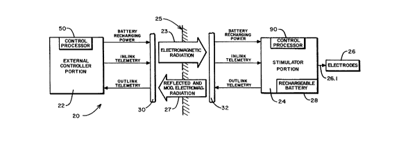
FIG. 1 is a simplified block diagram of the
regenerative electrical stimulator.
FIG. 2 is a block diagram of the external controller
portion.
FIG. 3 is a schematic diagram of the radio frequency
synthesizer of the external controller portion.
FIG. 4 is a schematic diagram of the modulator, the
driver, the class D power amplifier, and the receiver
portion of the external controller portion.
FIG. 5 is a schematic diagram of the power supply
circuity for the external controller portion.
FIGS. 6a and 6b are schematic diagrams of the control
processor integrated circuitry for the external controller
portion.
FIG. 7 is a schematic diagram of the integrated
circuits comprising the program memory circuitry of the
external controller>portion.
FIG. 8 is a schematic diagram of the static random
access memory and the real time clock circuitry of the
external controller portion.
FIG. 9 is a schematic of the circuitry for the
display interface of the external controller portion.
2~2~818
' - 5 -
FIGS. 10a and 10b are schematic diagrams of the
debugging port circuitry and keyboard connecting circuitry
of the external controller portion.
FIGS. 11a and 11b are schematic diagrams of the
personal computer interface circuitry of the external
controller portion.
FIG. 12 is a block diagram of the stimulator portion.
FIG. 13a is a schematic diagram of the passive
transmitter, envelope demodulator and threshold detector
for the stimulator portion.
FIG. 13b is a schematic of the power circuitry for
the stimulator portion.
FIG. 14 is a schematic of the t:ontrol processor for
the stimulator portion with related circuitry.
F3GS. 15a and 15b are schematic: diagrams of an
analog-to-digital convertor, switching circuitry and
connector circuitry.
FIG. 16 is a schematic of the system interrupt timer
and watchdog timer for the stimulator portion.
~:~~D~ ~~
_6_
i)~TA~hED DESCRIPTION O~' TiiiPR~Fi;I~R~D ~~iDOD3i~i~~IT~
A preferred embodiment of the invention is
illustrated in FIGS. 2-16.
FIG. 1 shows a simplified block diagram of the
regenerative electrical stimulator device 20. The
external controller portion 22 has a first antenna coil 30
located exterior the body. The stimulator portion 24 with
a second antenna coil 32 is intended to be surgically
implanted in the patient close to skin barrier 25. The
stimulator portion 24 connects by way of the cable 26.1 to
electrodes 26 which are placed in proximity to damaged
nerve tissue. The rechargeable battery 28 provides the
operating poorer for the stimulator portion 24 and provides
the power for the electrical stimuli presented to the
electrodes 26.
The first antenna coal. 30 emi~tev Plectromagnetic
radiation, represented as arrow 23, and is utilized for
the in-link and out-link telemetry f.'or the external
controller portion 22 and provides t:he power for
recharging the rechargeable battera~a 28. "In-link"
telemetry being defined as the transmission of signals by
the external controller portion 22 into the implanted
stimulation portion 24. "Out-link" telemetry being the
transmission of data out from the stimulator portion 24 to
the external controller portion 22. The electromagnetic
radiation is comprised of a modulated carrier wave
operating in the range of 2 megahertz (MHz) that crosses
the skin barrier 25 where it is received by the second
antenna coil 32.
The second antenna coil 32 is utilized for in-link
and out-link telemetry for the stimulator portion 24 and
CA 02120818 1998-O1-06
_ 7 _
also receives the power for recharging the batteries 28.
The out-link telemetry is accomplished by modulating
electromagnetic radiation which is reflected back to the
first antenna coil. The reflected electromagnetic
radiation is indicated by arrow 27. '
All of the functions of the external controller
portion 22 and the stimulator portion 24 are controlled by
their respective control processors.
External Controller Portion
FIG. 2 is a detailed block diagram of the external
controller portion. The principal circuits comprising the
invention are the receiver circuits 34, the transmitter
circuits 40, the first process controller 50, electrically
erasable programmable read only memories (EEPROMS) 52, 54,
a keyboard interface 56, a real time clock 58, the LCD
display circuitry 64, and a personal computer interface
60. The first antenna coil 30 connects to the transmitter
portion 40 which includes a modulator 42, a radio -
frequency (RF) synthesizer 44, a driver 45, and a class D
power amplifier 46.
FIG. 3 shows a schematic diagram of the RF
synthesizer of the transmitter portion 40 of the external
controller portion 22. The RF synthesizer 44 has several
subcircuits comprised of the voltage controlled oscillator
(VCO) 64, the phase locked loop 66, and the low pass
filter 68. The phase locked loop integrated circuit 67
utilized in the preferred embodiment is a Motorola~MC
145106. The integrated circuit 67 utilizes an external
crystal with a frequency of 10.240 MHz. The integrated
circuit 67 divides the 10.240 MHz frequency into an
internal reference frequency which is compared to the
trade-mark
CA 02120818 1998-O1-06
frequency of the voltage controlled oscillator 64. The
output of this comparison is the loop error voltage which
goes from the integrated circuit 67 to the low pass filter
68 where the reference signal frequency component is
removed. The error voltage is then applied to the voltage
controlled oscillator 64 to adjust the frequency of the
voltage controlled oscillator 64. In the preferred
embodiment, the frequency of the RF synthesizer 44 is set
at two l~Iz, however it is programmable by sending a
frequency programming command from the control processor
50 to the phase locked loop integrated circuit 67. The
programming connections of the integrated circuit 67
connect to the terminals on the CON1 connector 70. The
corresponding terminals of CON1 connector 70 are on
FIG. lla.
The output of the voltage controlled oscillator 64
goes via conductor 64.1 to the CMOS buffer amp 69, a Maxim*
MAX626SMD integrated circuit, which has dual outputs, one
output looping back to the integrated circuit 67 by way of
conductor 69.1 and the other output providing a w
symmetrical RF signal through conductor 69.2 for the
driver amplifier 72 and the power amplifier 46.
Referring to FIG. 4, the driver 72 and class D power
amplifier 46 are shown. The driver amplifier 72 consists
of a pair of bipolar transistors 72.1 and 72.2 and
receives the RF signal from conductor 69.2 after it has
passed through the buffer amplifier 71. The power
amplifier is comprised of a pair of IRF510 power MOSFETS
46.1, 46.2 configured as a class D power amplifier 46.
The output of the class D power amplifier 46 is connected
through conductor 46.3 to a series resonant tank circuit
comprised of the capacitors 75 and the first antenna coil
30. The first antenna coil 30 radiates the RF energy and
*trade-mark
CA 02120818 1998-O1-06
_ g _
couples with the second antenna coil 32 of the stimulator
portion 24 when they are in proximity to each other. The
tank circuit thus constitutes a tuned primary circuit 31.
The two MHz radio frequency (RF) signal provides the power
transfer for recharging the batteries of the,implanted
stimulator portion 24.
The in-link telemetry modulation is provided by the
modulator 42 which acts to switch the output of the
voltage controlled oscillator 64 to ground, thus grounding
the RF signal and eliminating the RF input to the-drive
amplifier 72 and the power amplifier 46. The modulator 42
in the embodiment shown consists of two SiliconiX*Si9955
metal-oxide-semiconductor field-effect transistors
(MOSFETS) 42.1, 42.2 connected between the ground and the
conductor 69.2, shown in FIG. 3. The operating signal for
the modulator 42, designated "ETX" on FIGS. 3 and 4, is
received by way of conductor 69.3, and is the serial data
output from the control processor 50 containing the
commands to be sent to the stimulator portion 24. The
serial data operates to amplitude shift key the radio
frequency output of the power amplifier 46. Conductor
69.3 connects to the CON1 connector 70 with the
corresponding conaecting,terminal shown on FIG. lla. The
serial data output constituting the in-link telemetry signal
is designated "TX" on FIGS. 6b, 10a, lOb, lla and llb.
w The receiver or out-link telemetry circuitry for the
external controller portion 22 is also shown on FIG. 4.
The secondary of the transformer 78, and capacitor 7-9,
form a tuned circuit. The transformer 78 has a single
turn primary which picks up the current in conductor 46.3
and induces a voltage in the secondary of transformer 78.
The voltage induced in the secondary of 78 fluctuates in
accordance with the out-link telemetry signal from the
*trade-mark
F
- to -
stimulator portion 24 GIhiCh is comprised of reflected RF
energy. The method of reflecting and modulating the RF
energy in the stimulator portion 24 is discussed below
with reference to FIG. 13a.
Continuing to refer to FIG. 4, the envelope
demodulator circuitry 36 detects the encoded signal,
filters the rf, and provides the signal to the tracking
and threshold detector 38. The tracking and threshold
detector 38 compensates for variations in positional
alignments between the first antenna coil 30 and the
second antenna coil 32 and also compensates for motion
between the coils 30, 32 during operation. The tracking
and threshold detector 38 utilize three operational
amplifiers 38.1, 38.2, 38.3 configured as an automatic
gain control with a threshold crossing detector. The
three operational amplifiers are available from Motorola
Inc. and are identified as MC33:~72D, MC33172D, and LM31:1
respectively. The third operationaa. amplifier 38.3
operates as a comparator, comparing an averaged value of
the pulsed wave form to the actual serial pulse wave form,
the output providing stable, uniform serial data pulses.
The serial data pulses are then for~rarded to the micro-
controller 50 for processing.
FIG. 5 shows a schematic of a programmable power
supply for the external controller portion 22. The power
supply supplies the necessary power for all of the
circuits of the external controller portion 22. Notably,
the output of the power supply is programmable to provide
incrementally adjustable voltage to the class D power
amplifier 46 by way of commands from the control processor
50 to integrated circuit 49 thereby adjusting the RF
output level. Iwtegrated circuit 49 is a CMDS analog
switch available through Maxim Integrated Products, 120
- 11 -
San Gabriel Drive, Sunnyvale, CA ~~.086. The power supply
requires 12 volt input at terminal 22.7. The control
lines for the integrated circuit 49 connect to the CON2
connector 49. The CON2 connector 49 with the connecting
terminals is on FIG. 11a.
FIGS. 6a, 6b, 7, 8, 9, 10a, 10b, 11a and 11b show
schematic drawings of the control processor circuitry and
the related operating and me:a~.ory circuitry for the external
controller portion 22. The various signal lines on the
figures showing the digital circuitry, FIGS. 6a, 6b, 7, 8,
9, 10a, 10b, 11a, 11b, 14, 15a, 15b and 16, are labeled
with conventional terminology. The labels enclosed in
ovals indicate that that specific line connects to all
other like-labeled lines. The control processor 50
ut3.li~ed in the preferred embodiment is a Motorola. Inc. MC
68332 integrated circuit. The MC 68332 is a 32 bit micro-
controller w:Lth 2K bytes of fast static R.AM, an
asynchronous serial interface, a synchronous serial
interfac~, a time processor unit, e~even interrupt lines,
chip select outputs, and bus control circuitry.
For specific information on the speoifications, the
technical information, and the details of programming and
operation of the MC 68332, see I7sex~'s Manua.Z, document Plo.
MC 683324M/AD, by Motorola, Tnc., distributed by Motorola
Literature Distribution, P. O. Boy 20512, Phoenix,
Arizona; and also see the MC 68332 Motorola Semiconductor
Technical Data, document N~. MC 68332TS/D, 1990, also
distributed by Motorola Literature Distribution.
As shown in FIG. 8, the address bus 53 and data bus
51 connect the first control processor 50 to the system
static PAM 55 comprised of four HM628128 integrated
circuits. FIG. 8_also shocas the real time clock 58 with
. .: . .. ; ::.,, ., y . .
.; ~ : ,
~ .
.
~
'
.:
:
:
" ;:,.,
.: ;
h .
4 ..
.
.
,
... ..: ; ~:< v:::., .;. ; ...,: ...
,.: ;, .;. .: ,.v:-. : ... : ,: ;> ;:;.'.
:. .
.,,;":.... ;.;~ i; .,...._.,,, :; , ;,. .,.: :
. -:;; .'.:;, ....:.::.::~: ~~ :~ :;;~ v . '
,
. ,
~ ~=
~
~
. :!. ~
., ,..
~~ .
:~ ~,,. ~ ,,.
.
~. ~;
~ :
::
~':
,,
. .
r. ,
. >
. ,.
,3a ,
, .
.
.;
... . .
,..
a :: r ~ .:;.
'
'. ;.;
.. .. : ';. ,:' . , '.
- 12 -
battery back up allowing data recorded to be time stamped.
As shown in FIG. 7, the address bus 53 and data bus 5~.
also connect the first control processor 50 to the program
ROM circuitry 57 comprised of four 28F020 FLASH EEPROM
(electrically erasable programmable read only memory)
integrated circuits. The FLASF~I memory allows the
programming to be stored indefinitely. The Programs may
be modified by way of a personal computer serially
connected to 'the first control processor 50 by way of the
personal computer in~erfa~ce 60 shoc~a~. in FIGS. 11a ~d llb.
FIG. 9 shows the LCD display circuitry 64. The LCD
is not shown but is of conventional design and is
connected by way of the J4 connector 64.2. Contrast is
controlled by way of a digital/analog converter 64.1
manufactured by Analog Services, Inc., ~ne Technology Way,
Norvaood, Massachusetts 02062.
FIG. 10a shows the circuitry for the downloading and
debugging port for connection with an external personal
computer through the J1 connector 60.5. The serial data
signals containing the in-link and out-link telemetry data
designated '°TX" and "RX°' go through the 232 c~nverter
60.5, manufactured by Maxim Integrated Products, Inc., for
compatibility with the personal computer. Similarly, the
other signal lines to and from the first control processor
50 are appropriately conditioned. FIG. 10b shows the
circuit location for the keyboard switches (not shown) for
operating the external control portion 24 at the J2
connector 56. The signal lines 56.5 connect to the first
contral processor 50 shown on FIG. 6b. FIG. 10b also
shows the J3 connector 60.3 fcr connecting a power Cn/Off
switch (not Shown) and an '°enter°° switch (not shown).
~~.~~~1~
- 13 -
FIG. 11a shows the circuitry for interfacing the
device with a personal computer. The 25 pin J1 connector
60.7 provides the direct linkage with the personal
computer. Also shown are the CON1 connector 70 and the
CON2 connector 49 which connect the RF telemetry and power
supply circuits to the digital circuits and two latches
64.7, 64.8. FIG 11b shows an additional 232 converter
60.9 and terminals for the J2 connector 56 also shown in
FIG. 10a. The 232 converter 60.9 is also manufactured by
l~ia~im Integrated Products, Inc.
Antenna Coils
As previously indicated, the first antenna coil 30
couples with 'the second antenna 32 coil to
~transoutaneously provide power for recharging the
batteries of the stimulator portion 24 and to provide in-
link and out-link telemetry. The antenna coils are
configured in series tuned circuits which provide a low
impedance primary tuned circuit 31 which is desirable for
operation with the class D power amplifier 46 and a low
impedance secondary tuned circuit 33~ which is compatible
to the secondary tuned circuit load.
The design and specification of the first and second
antenna coils 30, 32 was dependant on the load presented
to the second antenna coil, the circuit configurations,
the coupling coefficient, the inductances and the desired
physical dimensions. An appropriate size for the second
antenna coil 32 for the implantable stimulator portion 24
was determined to be one inch. Extensive analysis and
experimentation yielded the values for the preferred
embodiment which are presented in Table ~. below.
1 v
.' , ~
- 14 -
TA~~~ 1
First Antenna second Antenna
Coil 30 Coil 32
Coil diameter 1.25 in. 1.00 in.
Axial thickness 0.125 in. 0.125 in.
Radial thickness 0.025 in. 0.025 in.
rlo. of turns 10 turns Z3 turns
Wire Lit Mire AWG ~Jo. 30 copper
Inductance 5.8 NCH 8.0 ~.H
The Litz wire for the first antenna coil is comprised
of single nylon polyester covered copper wire, 1.75 strands
of AWG 48, available from Kerrigan-hewis, Inc. The above
design provides adequate tolerance room far variation in
coil separation and misalignment. The design separation
between the coils is 1/4 inch, however, the device will
operate satisfactorily with significant variation from
this dimension.
The first antenna coil in the preferred embodiment is
encapsulated in silicon rubber and a.s connected by way of
cable to the external controller poi..~tion 22. Attaohment
to the skin of the patiewt for recharging and/or telemetry
may be accomplished by way of adhesive tape or other
products such as Tegaderm''~ available from Minnesota Mining
and Manufacturing Company, 8t. Paul, Minnesota. The
second antenna coil is included in the stimulator
encapsulated portion 24.
Implantable stimulator Portion
FIG. 12 shows a detailed block diagram for the
implantable stimulator portion 4. The second antenna soil
32 is connected to 'the battery charging circuits 80 for
providing the power to recharge the batteries 28; the
antenna coil 32 is connected to the envelope demodulator
82 and threshold detector 84 to provide the in-link
- .L 5 -
telemetry; and the antenna soil 32 is also connected to
the passive telemetry transmitter 86 to provide the out-
link telemetry.
The envelope demodulator 82 and threshold detector
84 input to the serial interface portion of the second ,
control processor 90 for processing the in-link telemetry.
Similarly, the serial interface of the second cowtrol
processor provides the out-link telemetry data to the
passive telemetry transmitter 86. The second control
processor 90 :further receives data from the charging sense
circuits 92, electrode current and voltage data from the
electrode current and voltage sense circuits 94. The data
is input into the analog-to-digital converter portion of
the second control processor 90. The second control
pracessor 90 controls the output of the electrodes 26 by
way of the digital/analog cirouits 98, the current mirror
97, and the analog switches 95.
FIG. 13a shows a schematic diagram of the circuitry
for a preferred embodiment for the passive telemetry
transmitter 86, the envelope demodu3.ator 82, threshold
detector 84, the battery charging circuits 80, and the
rechargeable battery peak 29. The y~econd antenna coil 32
is shown in series with capacitor 96 forming the secondary
tuned circuit 33. The secondary 'tuned circuit 33 is
connected to a full wave bridge rectifier circuit 93 and
filtering capacitors 93.1 which comprise the battery
charging circuits 80. The full wave bridge rectifier is
connected to the battery pack 29 by way of conductors 93.4
and 93.5. Tn the preferred embodiment, the batteries 81
are nickel metal hydride (Nil~iH) rechargeable battery
cells, size ~, and with a voltage output of 1.2 volts.
This type of battery provides an improved energy density
over other 'types of rechargeable batteries such as nickel
-:: : ::
:. r ~~ .:'
' :' % : ::
: ;
:: '
'
. . .. .
' ... ... . . .,
.. ., ;. ,., t. ,.. ..
' ..~.,. .:.1 ' ~...,s , .
".:..~ . . , " .
. :v..: ., ~'... . ;,:'.r . ~:~ n......:~: '.'.
' ::: ,. . ..'.~ . ~'~.~. .. . :':
. ':.,... ~. :.-.
\
.V.:W, ;. ~... , !;. .'i .;n ..., ;,:,. , :.."
. .:: ,''.':., . . ~: .': ~~.:.:~: .n W: .. .;.~:'.. . .
'a , ,: ' ' ,
:: : ;;
;
~
:
~
'
. : . , :: . . : .
' .. ...
' .. , .
: : . .. ;
.:: : :
: C ;
:
.,, ,:
"
'
~ . ,,,, ,... . .:;:: : :..;'. .::.
t , .i.. . ' ...~;. ;
:.:.; -'': '..
.,
, :: ,
. . .
: .
,
,;. .
,.. .. ,;,
: .. . .--.: ..n. .. ~..::...:.
::.::. , :' ~., -. ,
.; ...i: ..
:. ~:~ .,,...,, .:,.~,:~,:... .,
.::, :'. , .~,,
~ ~.; ;~
' '.'..
:~
-
:
..
, . .
... .. ,.. . ,..
. . ,
.. ,..
. ., ,
".
..
"
,.: . .: ..
' .. ' ,
'
,
' . . :v .... ,.. : ; .~ .. n .:: . :.
s ..... ~ , . , .:;
~ :
t
21
?
'
911:. , .:. ~ ~ .. , .
; ~
.
. , . (,~.' .
. ... . ,. ..
, '
..
. '. ~ . ,,
y ,.'. f
~ ~
fy ~:~5...:.
,n . . . '
:'.~.', ~ '
~ :~:. ' ~
: .
' ~~
' ; -
'
'
~
. ., : ;; . .
h.::. ~ ,
: ..: :. ,.. .
1, . '..'.:'.,.,...,.:
, . ..:,.,... ~ ...~ .
... .. :: :
....... . ...~ ... ..... ,... ,.,
.; . ..... . . " . ..
....... .. ., ..
.. .,.,~...,.y., . m. ~. '.... .,..;:.
,:.', ' . ...., .; ,. .. ,
.... , . .. .... ... ..
16
cadmium {NiCd) batteries, ef the same size. The Nit4I-I
batteries are available from Iiarding Energy Systems, Inc.
The battery pack 29 also includes circuit breakers 29.1 to
protect against excessive current. The devices in the
preferred embodiment are identified as T4040 PTC,
manufactured by the Thermacon Company, and are solid state
and automatically reset. Also included in the battery
pack 29 is a temperature sensor 92.1 for monitoring
battery temperatures while recharging. The temperature
sensor along with conductors 92.2, 92.3, 92.4, and 92.5
comprise the charging sense circuits. Conductors 92.4 and
92.5 are connected to the temperature sensor 92.1.
Conductors 92.2 and 92.3 are connected to the battery
cells 81.
The passive telemetry transmitter 86 is comprised of
a pair of MOSFET transistors 86.1, 86.2 which are
connected across the tuned secondary circuit 33 so that
when they are switched "on" the tuned secondary circuit 33
is short circuited. The first antenna coil 30 and second .
antenna coil 32 couple when they are in proximity to each
Other. The short circuiting of the tuned secondary
circuit 97 operates to reflect electromagnetic radiation
back to the tuned primary~circuit 31 which is otherwise
absorbed by the tuned secondary circuit 32 and connected
circuitry. The MOSFETS 86.1, 86.2 are switched in
accordance with a signal conveyed on conductor 86.5 from
the second control processor 90 to generate the encoded
owt~link telemetry signal labeled "TX" on FIG. 13a.
Conductor 86.5 connects to J11 connector 99 which has
correspc~xidixig terminals shown ors FIGS. 16a and 15b.
The P~i~SFETS 86.1, 86.2 shown in the preferred
embadiment of the passav~e transmitter are Silic~nix Si9955
transistors. In that these ~iOSFET switches have extremely
- 17 -
low power drain and the actual medium which is utilized to
transmit the out-link telemetry is RF power reflected from
the external controller portion 22, the transmitter is
passive and the battery consumption of the out-link
telemetry is negligible. The MaSFETS are operated by the
second control processor 90 at a rate of X800 baud.
The envelope demodulator and threshold detector 82 is
also shown on FIC. 16a. Transformer 85 has a single wire
primary 85.6 and a secondary that is in parallel with
capacitor 85.1 forming a tuned circuit. The tuned circuit
is connected to a pair of diodes 85.2 and additional RC
circuitry whereby the in°lin3~ telemetry signal is detected
and shaped. The signal then goes to the threshold
detector 8~ c:omprised of a MaSFET. The threshold detector
8~1 presents t:he received in-link telemetry signal labeled
~~RX" to the second control processor 90.
The conductors for the envelope demodulator and
threshold detectar 82, and the charging sense circuits 92,
connect to the connector 99 which has the corresponding
texxn~.nala showrx in FIGS. 15a and 15b.
FIG. 13b shows the circuitry f:or system voltage and
boost converters 91 for the implant:able stimulator portion
24. ~3attery voltage of 2.2 volts is provided from
conductor 91.1. The 2.2 volts is boosted to provide
system power and the power for the electrodes 26. Power
output for the electrodes 26 is switched by way of the
MOSFETS 92.5, 91.6 and is controlled by the second control
processor 90. The terminal connections for the system
voltage boost converters circuitry 91 is also at the
connector 99 with the corresponding terminal connections
shown a.n FIGS. 15a and 15b.
~~~f~,3.io
- 18 -
FIG. 14 shows the second control processor 90 and
related circuitry. The second control processor 90 used
in the preferred embodiment is a Motorola Semiconductor
Inc. microcontroller No. ~8I3C805C4. The microcontroller
has a system RAM, bootstrap ROM, EEPROM bank A, EEPROM
bank E, a synchronous serial port, 24 general input/output
pins and an interrupt controller. For specific
information on the details of operation, programming,
technical information, and specifications, see Motorola
Semiconductor Technical Data, document No. AD1991R2, by
Motorola, Inc., 1985, distributed by Motorola literature
Distribution.
FIC. 14 also shows the digital analog circuitry 98
comprised of the DAC8143 D/A converter 98.1, current
reference integrated circuit 98.2, the current mirror 97,
and the analog switches 95. The second control processor
90 is connected to the analog switches by way of electrode
drive bus 90.5. The drive bus 90.5 connects to the
operating terminals 95.1 of the analog switches 95. The
output of the analog switches goes t:o the electrode cable
2f>.1 and the electrodes 26.
The current reference integrated circuit 98.2
supplies a maximum reference current to the converter. In
the preferred embodiment 400 SSA was used. The
digital/analog converter 98.1 provides 100 output current
levels at output 98.5. This output is presented to tine
current mirror 97 which provides a constant current source
independewt of the load with a gain of four. The control
processor 90 directly controls the digital/analog
converter 98.1
~'IG. 15a shows an analog-to-digital converter
iwtegrated circuit 80, with inputs for battery voltage
';:. . .. ::,... , ::. .':~ '~'~i :'..... ............. ...: ,..' ,,..:'
S
1 7.
.... . , . .. . ." ..; i t :.',, ,... .,.'.°. ..~~,, r:r
.;. ~ .::. ;' , v. ~~ . , ':~~' ... r,
' ~.. .. ~ ' ' . ~ . ,.." .., ' : :'.
,.. ..,.. .. ',,... .. , r . . , ~~: L'... ~:. . .. ,.... , .~
.~. . .'. ~ .':, ' ; ' . ~:'~. , , , :.. ~ ".,~;.. '. , n , ~.: ~ , "~'. .
.:,... , . '~. . , .~:~~ . r~:' ' . ~.: ". '....'
- 19 °
80.1, 80.2, battery temperature 80.3, electrode drive
voltage 80.4, receiver RF signal strength 80.5, and
circuit board temperature 80.6. Ttae output 80.7 of the
converter 80 goes to the second control processor 90. The
control processor 90 selects the specific parameter to
input by way of "DIId" line 80.8. Notably, power to the
converter 80 and the various inputs and outputs is
switched under the control of the control processor 90.
FIG. 15 shows the connections to the J11 connector 99.
operation of specific circuits was discussed in
reference to the figures. An overview of the operation of
the stimulation and telemetry functions is as followsc
The electrical stimulus to the neural tissue is
provided by the electrodes 26 attached to the stimulator
portion 24. The potential to the electrodes 26 is
prorrided through the analog switche:3 95. The second
control processor 90 is appropriate7ly programmed to
control the analog switches to generate the stimuli with
the specified parameters, i.e., monophasic, bi-phasic,
direct current pulses, and with the specified amplitude
and duration.
The parameters of the stimuli are changed by way of
digitally encoded commands from the external controller
portion 22 through the in-link telemetry system.
The in-link telemetry is accomplished by the first
control processor 50 being programmed to encode commands
and operate the modulator 42 to amplitude shift key the RF
signal generated by RF synthesizers 45. The modulated RF
signal goes to the first primary tuned circuit 31 which
includes the first antenna coil 30. The first antenna
coil 30 and second antenna coil 32 couple when in
~l
- 20 -
proximity to each other transferring the RF energy to
tuned secondary circuit 33 of the stimulator portion 24.
The envelope demodulator 82 and threshold detector 8~
detect and shape the encoded signal by way of the
rectifier, RC circuitry, and transfers the signal to the
second control processor 90.
The second control processor 90 in the stimulator
portion 24 is programmed to receive and decode the
commands and controls the analog-to-digital converter 98.1
and the analog switches 95 to alter' the stimuli parameters
as commanded.
The first central processor 50 in the external
controller portion 22 also is programmed to send commands
requesting data on the battery voltage, battery
temperature, circuit board temperature, electrode voltage,
and the stimuli parameters. The second central processor
90 is programmed to enable the anale~g-to-digital converter
80 and the appropriate sensors to receive data on the
requested conditions. Tine second control processor then
encodes the data and operates the out-link telemetry to
transmit the data to the external ccmtraller portion.
Cut--link telemetry transmissiar~ is accomplished by
the second control processor 90 switching the M~S~'~TS 86.1
and 86.2 c~N and CfF in accordance with encoded data when
the first and second antenna calls are coupled. The
switch short circuits the tuned secondary circuit 33 and
reflects back RF energy to the first antenna coil 30.
The external controller partian 22 receives the
encoded out-link telemetry signal, and detects and
demodulates the signal by way of the receiver circuitry
34. The first control processor 50 then decodes the data
:':
~~~~~~8
' ° 21
and stores the data in the system static RT~PI 55 and/or
enables the LCD display circuitry 64 to display the data.
The present invention may be embodied in other
specific forms without departing from the spirit or
essential attributes thereof, and it is therefore desired
that the present embodiment be considered in all respects
as illustrative and not restrictive, reference being made
'to the appended claims rather than to the foregoing
description to indicate the scope of the invention,