Note: Descriptions are shown in the official language in which they were submitted.
2 1 2 0 8 7 5
DURAB~ T~-EMI88IVITY 80T~ CONTROT
T~IN FILM COATING
Inventors: Jesse D. Wolfe
Abraham Belkind
5Ronald E. Laird
R~ckaround of the Invention
ThiC invention relates generally to visibly
transparent infrared reflecting interference filters,
and more particularly, to a durable low-emissivity
filter.
The use of transparent panels in buildings,
vehicles and other structures for controlling solar
radiation is quite prevalent today. The goal of solar
control is to transmit light while excluding much of the
solar energy, thus decreasing the amount of air condi-
tion or cooling required, and conserving energy. In
addition, modified glass as a ~tructural material
provides the color flexibility architects desire.
Various processes have been employed to alter
the optical properties of these panels, including
coating glass or plastic substrates by various tech-
niques such as electrolysis, chemical vapor deposition
and physical vapor deposition, including sputtering with
planar magnetrons. For instance, thin metal films have
been deposited on glass or plastic to increase the
reflectance of solar radiation. Windows deposited with
a multi-layer dielectric-metal-dielectric coating that
exhibits high visible transmittance, and high reflec-
tivity and low emissivity in the infrared range, are
even more energy efficient. The index of refraction of
the dielectric layer is preferably 2.0 or greater in
..... . . . .. . . . .
2 1 2 08 7 5
order to minimize the visible reflectance and enhance
the visible transmittance of the window. This dielec-
tric layer which often consists of metal oxide coating
also offers additional protection to the fragile metal
films. The optical properties of p~nels can also be
modified by altering the composition of the substrate
material. Nevertheless, interference filter panels
manufactured by the above-described methods have been
only partially successful in reflecting solar radiation
to the degree required for significant energy conser-
vation. For example, Apfel et al., U.S. Patent
3,682,528, issued August 8, 1972, described an infra-red
interference filter with visible light transmission of
only approximately 72% and with infra-red transmission
of approximately 8%.
Another problem associated with interference
filters is their structural integrity, particularly
their inability to withstand harsh environmental condi-
tions. Current transparent panels having high reflec-
tivity for solar radiation are unsatisfactory in thatthe panels are subject to chemical and mechanical
degradation.
Summary of the Invention
It is a primary ob;ect of the present
invention to provide a durable, thin-film interference
filter which transmits visible light while reflecting
infrared radiation.
It is another object of the present invention
to provide a low emissivity interference filter with an
emissivity of about 0.1 and better than 82% transmission
in the visible region.
These and additional objects are accomplished
by the present invention which provides a durable, thin-
film interference filter which comprises a transparent
substrate onto which is deposited a first dielectric
2 1 2 08 7 5
layer, followed by metal and second dielectric layers.
In between each of the dielectric and metal layers i8
deposited a precoat layer that promotes adhesion between
the dielectric and the metal.
One aspect of the invention i8 the use of a
nic~el and chromium nitride for each of the metal pre-
coat layers. The Ni-CrNx films are thin 8c that there
i8 less absorption of visible light, but yet maintains
good adhesive properties. Another aspect of the inven-
tion is the use of silver as the metal layer. Specif-
ically, silver is sputtered in an atmosphere containing
a mixture of nitrogen and argon or other inert gas. It
was found that the presence of nitrogen produces a
silver layer that is more durable than silver films
sputtered in an atmosphere containing essentially pure
argon.
In one preferred embodiment, the interference
filter comprises a glass substrate onto which is
deposited a thin-film design consisting of five layers,
namely: titanium dioxide, nickel-chromium nitride,
silver, nickel-chromium nitride, and silicon nitride.
Another preferred embodiment of the
interference filter comprises of a five layer 6tructure
wherein one or both of the dielectric layers is formed
of a composite material containing zirconium nitride and
silicon nitride. It wa~ found that mixing zirconium
nitride with silicon nitride creates a composite layer
that has a high refractive index and excellent trans-
parency in the visible region. ~oreover, the optical
properties of this composite layer can be adjusted by
varying the relative amounts of zirconium nitride and
silicon nitride.
The dielectric layers of the inventive
interferences filters can be reactively sputtered by a
rotatable cylindrical maqnetron. Composite layers can
be formed by cosputtering from dual cathode targets or
4 2~ 208 7 5
from one or more alloy targets. A feature of the
inventive process i8 that by reducing the intrinsic
stress of the ~econd dielectric layer, an extremely hard
and chemically resistant thin film coating is produced.
In sputtering silicon nitride as the second dielectric
layer, it was demonstrated that the intrinsic stress of
this layer can be reduced by orienting the magnetic
assembly of the cathode at an acute ~ngle Vi8-~-ViS the
substrate.
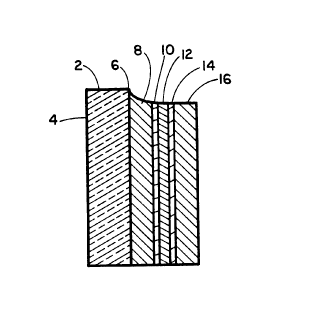
Brief Description of the Drawings
Figure 1 is a cross-sectional view of a five
layer design thin-film interference filter produced in
accordance with this invention.
Figure 2 is a cross-sectional view of a
magnetron device.
Figure 3 is an EDS spectrum for a Ni-CrNx
film.
Figure 4 is a graph of percentage transmission
versus wavelength for Ni-CrN~ films.
Figure 5 is a graph of percentage transmission
of silver films versus nitrogen concentration in the
atmosphere in which silver metal was sputtered.
Figure 6 is a graph of percentage transmission
versus wavelength for interference filters having
different silver metal thicknesses.
Figure 7 is a graph of percentage transmission
versus silver metal thickness and emissivity.
Descri~tion of the Preferred Embodiments
A thin-film interference filter incorporating
the present invention is shown in Figure 1. The filter
comprises of a transparent substrate 2 which is provided
with two planar parallel surfaces 4 and 6, in which sur-
face 4 is exposed to the medium and surface 6 is coated.
The substrate can be formed of any suitable transparent
-
a~ 208 7 5
material; however, the substrate is preferably a
material which ha5 superior structural properties and
minimum absorption in the visible and near-infrared
spectra regions where the solar energy is concentrated.
Crystall~ne ~uartz, fused silica, soda-lime silicate
glassj and plastics such as polycarbonates and
acrylates, are all preferred substrate materials.
Deposited onto the substrate surface 6 is a
first dielectric layer 8 that is preferably made of a
material having an index of refraction of greater than
about 1.5, and more preferably between 2.1 and 2.S or
higher. Suitable dielectric layer materials include
metal oxides such as titanium dioxide, niobium penta-
oxide (Nb205), tin oxide, zinc oxide, indium oxide
(optionally doped with tin oxide), bismuth oxide, and
zirconium oxide. See Hart, U.S. Patent 4,462,883,
issued July 31, 1994. Yet another suitable material is
silicon nitride. Another suitable dielectric material
comprises a thin composite film containing zirconium
nitride and silicon nitride (collectively referred to
herein as "SiZrN") that is fabricated by cosputtering
from dual targets or from a single alloy target of a dc
cylindrical magnetron.
2 5 Besides SiZrN, composite films comprising
titanium nitride and silicon nitride (collectively
referred to herein as "SiTiN") or comprising hafnium
nitride and silicon nitride (collectively referred to
herein as "SiHfN") can also be used. SiTiN and SiHfN
composite films are also prepared by cosputtering from
dual or single targets. Finally, a composite film
comprising a mixture of silicon nitride, aluminum
nitride, zirconium nitride, titanium nitride, and/or
hafnium nitride can be used as the first dielectric
layer. The refractive index of the composite films will
vary depending on the relative amounts of the different
21 208 7 5
nitrides that comprise each film. It has been found
that when silicon nitride is used as the first dielec-
tric layer, the visible light transmission of the
inventive filter is slightly less than the transmission
when titanium dioxide or a composite film is used,
particularly if the silver metal layer is equal to or
greater than approximately 100 ~ in thickness.
One method of depositing composite films is
cosputtering of a cylindrical magnetron employing dual
targets with one target being made of silicon and the
other target being made of either zirconium, titanium,
hafnium, or mixtures thereof. When cosputtering with
dual cathodes with nitrogen as the reactant gas, the
angle of the magnetic assembly of each target can be
adjusted to get homogeneous composition distribution.
A description of a method for cosputtering composite
films from a magnetron device having dual cathode
targets is found in EPO application 0 560 534 A1
published 15 September 1993 and U S Patent 5,377,045
issued 27 December 1994
Generally, the thickness of the first
dielectric layer ranges from approximately 250 to 450 A,
and more preferably from approximately 280 to 330 A.
When TiO2 is used as the first dielectric layer, the
thickness of the layer preferably ranges from
approximately 200 to 400 A, and more preferably from
approximately 250 to 330 A.
As shown in Fig 1, the inventive filter next
comprises of a first metal precoat 10 that is deposited
over the first dielectric layer. Precoat layer 10 is
preferably maintained as thin as possible so that it will
have very little, if any, adverse effect upon the optical
characteristics of the filter or the subsequent metal
layer Precoat layers with thicknesses ranging from
approximately 5 to 20 A have been satisfactory
-
7 2! 2 08 7 5
Preferably, the first metal precoat layer comprises a
mixture of nickel metal and chromium nitride tdesignated
as Ni-CrNx or nickel/chromium nitride) with a thickness
between approximately 8 to lS A. Alternatively, the
precoat can comprise of nickel-chromium alloy preferably
comprising approximately 20% to 90% nickel and approxi-
mately 10% to 40% chromium; and more preferably the
alloy content is approximately 80% nickel and 20~
chromium. The alloy may contain small amounts (up to
approximately 15%) of other metals as well. An alloy
containing approximately 5%-15% molybdenum is believed
to further increase the chemical durability of the
precoat layer. Nichrome (or NiCr) shall refer to alloys
having various ratios of nickel, chromium, molybdenum,
and other metals that can be used as the precoat layer.
Next, a partially reflective metal layer 12 is
deposited onto the first precoat layer. The metal layer
reflects infrared-radiation, yet allows for sufficient
visible light transmission. The metal layer can be
formed from a number of materials, with silver being
particularly satisfactory. Other metals that can be
utilized include gold, copper, and platinum. The thick-
ness o~ the metal layer ranges from approximately 80 to
150 A, and more preferably, from approximately 100 to
125 A. When the metal layer comprises silver, the
thickness should be from approximately 80 to 150 A, and
more preferably from approximately 90 to 125 A.
A second metal precoat layer 14 is then
deposited onto the metal layer which is followed by the
final dielectric layer 16. This second metal precoat
layer can also comprise a nickel-chromium alloy (as
described above for the first precoat layer) but more
preferably comprises a film of Ni-CrN~. The second
precoat layer has the same thickness ranges as that of
the first precoat layer.
2 ~ 2 08 7 5
The second dielectric layer preferably
comprises silicon nitride formed by reactively
sputtering a cylindrical magnetron. This layer has a
thickness from approximately 200 to 500 ~, and more
S preferably from approximately 400 to 450 ~. The above
described composite films can also be used although the
relative proportion of silicon nitride in each film
should be adjusted so that the refractive index ranges
preferably from approximately 1.98 to 2.08 (550 nm).
When a composite film is used, its thickness should be
from approximately 300 to 500 ~, preferably 400 to 450
A. However, whether silicon nitride or a composite
substance is used as the second dielectric layer, the
layer most preferably should exhibit low intrinsic
stress. It was found that by reducing the intrinsic
stress of the second dielectric layer, an extremely hard
and chemically resistant thin film coating is produced.
To provide additional protection to the inventive
filter, a plastic laminate can be applied to the filter
of Fig. 1. See Young et al., U.S. Patent 4,965,121,
issued October 23, 1990.
The precoat, metal, and dielectric layers were
deposited with a d.c. magnetron. The dielectric layers
were prepared by dc-reactive sputtering with a rotating
cylindrical magnetron. A description of a cylindrical
magnetron suitable for depositing substrates with the
dielectric materials is found in Wolfe et al., U.S.
Patent 5,047,131, issued September 10, 1991.
A cylindrical or planar magnetron wherein the
target material is nichrome can be employed to reactive-
ly sputter the Ni-CrNx film in an atmosphere comprising
of nitrogen and an inert gas such as argon. At typical
dc-sputtering temperatures, nickel does not form
nitrides. (Without the nitrogen gas, a film comprising
~,~
2 ? 2 08 ~ 5
of nickel and chromium would be deposited instead.)
Alternatively, the Ni-CrNx film can be deposited by
using a magnetron with dual cathodes wherein one of the
cathodes has a nickel target and the other has a
chromium target to reactively sputter the Ni-CrNx film.
With respect to the metal layer, it was also
found that sputtering a silver metal layer in an atmo-
sphere containing some nitrogen produced interference
filters having improved environmental and optical
properties vis-à-vis filters in which the silver was
sputtered in an atmosphere containing no nitrogen or in
an atmosphere containing essentially pure nitrogen.
In depositing silicon nitride as the second
dielectric layer with dual rotatable cylindrical
magnetrons, it was found that the intrinsic stress of
the silicon nitride layer can be reduced by orienting
the magnetic assembly of each cathode at an acute angle.
As shown in Fig. 2, which is a cross-sectional schematic
view of a magnetron having dual cathodes 20A and 20B
positioned in vacuum chamber 22. Each magnetic assembly
18 has a "W" configuration with three elongated
magnetics 24, 26, and 28. The permanent magnetics
formed an unbalanced system which is typical for
rotatable cylindrical magnetrons. The magnetic assembly
of cathode 2OA is oriented at an acute angle ~1 of
approximately 45~ so as to direct sputtered material
towards the substrate 21 as it enter~ the deposition
chamber. Similarly, the magnetic assembly of cathode
20B is oriented at an angle ~2 ~f approximately 45~.
Each of angle ~1 or ~2 can range from approximately 20~
to 60~ independently, more preferably about 30~ to 50~
and most preferably about 45~. Each cathode is approx-
imately 2.5 inches (6.35 cm) from the substrate and the
center of cathode 20A is approximately 8.5 inches (21.59
cm) from the center of cathode 20B. Silicon nitride
layers so deposited have approximately one-fourth the
lO 2 1 2 08 7 5
intrinsic stress of silicon nitride layers produced when
the assembly is at a normal angle relative to the
substrate. It is not n~ceseAry that dual cylindrical
cathodes be employed to reactively sputter Si3N~ ~ut, if
a single cathode is used, it is preferred that cathode
2OA be employed with the substrate moving towards it.
The device as shown in Fig. 2 can also be used
to reactively cosputter composite films such as SiZrN.
For instance, one cathode could have a silicon target
and the other cathode could have a zirconium target.
F~verimental Results
A low-emissivity interference filter having
the structure as shown in Fig. l comprising a glass
substrate, a titanium dioxide first dielectric layer,
nickel/chromium nitride precoat layers, a silver metal
layer, and a silicon nitride second dielectric layer was
fabricated in an in-line magnetron system. The system
comprises of five sources of sputtering arranged in
series, with each sputtering source depositing one of
the five layers of the filter. The second, third, and
fourth sputtering sources comprised a planar magnetron
housed in a vacuum chamber for depositing the first
precoat, metal, and second precoat layers respectively.
The planar magnetrons, each comprising of a model HRC-
3000 unit, were manufactured by Airco CoatingTechnology, a division of assignee. The first and fifth
sputtering source each comprised a cylindrical magnetron
having dual targets to deposit the dielectric layers.
Each cylindrical magnetron comprised dual C-Mag~ model
3000 cathodes, also manufactured by Airco.
The targets of each cylindrical magnetron were
conditioned using an inert gas, thereafter the process
gas was added until the desired partial pressure was
reached. The process was operated at that point until
the process was stabilized. The substrate was then
r _
' 21208 75
- 11
introduced to the coat zone of the first cylindrical
magnetron and the film was applied. The substrate used
was soda lime glass.
For depositing a first dielectric layer
S comprising of titanium dioxide, the magnetron employed
a pair of titanium targets. It is known that Tio2 is
the predominant form of titanium oxide created in the
sputtering process. However, it is believed that other
forms are produced as well. Thus, unless otherwise
lo stated, TiO2 will represent all forms of titanium oxide
produced. TiO2 is particularly suited as the first
dielectric layer since its index of refraction is 2.50
(550 nm). Using Tio2 results in an interference filter
with a transmission of approximately 2% better than if
silicon nitride had been used. Argon was the inert gas
and oxygen was the reactant gas.
When reactively sputtering silicon nitride as
the second dielectric layer in the cylindrical magnetron
as shown in Fig. 2, argon was used as an inert gas and
nitrogen was used as the reactant gas. Other inert
gases can be used. (All forms of silicon nitride will
be represented by Si3N4.) The partial pressure of the
gas was determined by the transition from the nitride
mode to the metallic mode. Experiments were run as
close to that transition as practicable. The pressure
and flow rate of the sputtering gases were controlled by
conventional devices. Because the electrical conduc-
tivity of pure silicon i8 SO low that it is unsuitable
for sputtering with direct current, each silicon target
was impregnated or doped with a small amount of
aluminum. The magnet assembly of each cathode was
oriented at an angle of approximately 45~ from normal.
With nitrogen as the sputtering gas, the coating
contained a mixture of aluminum and silicon nitrides.
All of these components are relatively hard and form an
amorphous film that acts as a strong barrier. However,
21 2 08 7 5
.
12
the amount of aluminum in the film did not interfere
with formation of the desired silicon based compound
films. The stoichiometry of the silicon nitride formed
has been found to be close to the theoretical 3:4 ratio
for Si3N4.
For depositing each of the Ni-CrNx film
precoat layer~, a planar magnetron employing a nichrome
target was used. The nichrome used comprised approxi-
mately 80% nickel and 20% chromium. The gas mixture
comprise approximately 60% nitrogen and 40% argon.
Nickel sputtered from the nichrome target did not
nitride, but the chromium sputtered apparently did. The
film so produced is amorphous, chemically resistant,
electrically conductive, and extremely hard and durable.
It was found that with respect to the inventive thin
film interference filters, when Ni-CrNx is used, the
precoat layer(s) can be approximately 40% thinner than
NiCr, and yet the filters will still maintain the same
durability. In addition, by reducing the thickness of
the first and/or second metal precoat layers, the
overall transmission of the interference filter for
visible light increases. However, for interference
filters that may be subject to harsh environments, each
Ni-CrNx precoat layer should have a thickness of at
least about 8 A since it was found that interference
filters with thinner precoat layers often failed the
salt fog test and/or the humidity tests. In order to
avoid sputtering excessively thick metal precoat layers,
shields or baffles should be employed in the vacuum
chamber of the magnetron device to intercept some of the
sputtered material and to control the rate of deposition
onto the substrate.
For depositing the silver metal layer, a
planar magnetron with a silver target was used. The
sputtering occurred in an atmosphere containing 60%
nitrogen and 40% argon.
~ 21 a 08 7 5
13
Table 1 sets forth typical process data for
deposition of an inventive filter with the in-line
magnetron system. It is recommended that the HzO has a
partial pressure of less than or egual to 10-7 Torr in
the 6ystem. This can be ~ccomplished by conventional
means including the use of meisner-coils to con~en~ the
water, or high vacuum pumps. Other measures include
backfilling the system in nitrogen for 8 to 20 hours
before reactive sputtering at a pressure of approxi-
10 mately 1 ~.
TABLE 1
Flo~- Flo~- Flo~- Flo~-
Thick- r~te r~te r-t- r~t~ Poten- Pre~-
nts~ ~SCC~) ~SCCM~ ~SCC~) ~SCC~ ti~lPo~er ~ure ~o.
~Y~~I) Ar ~2~ e ~v) ~ u
Ti~2~8 10 0 102 0 -402 17 2.0 8
~i-Cr~8 ff 143 0 0 -452 6.5 2.5
1 5 ~9 1Z1 ff 143 0 0 -475 9.0 2.5
~i-Cr~x 8 95 1~3 0 0 -~52 6.5 2.5
Si3~4436 ~1 270 0 12 -451 11 ~.0
The addition of helium in the sputtering
process created additional atomic nitrogen through
peening ionization. It was found that the addition of
helium also decreased the amount of arcing at the
cathode targets which apparently resulted in improved
uniformity of the deposited film.
A comparison of the inventive filter to prior
art filters with respect to optical properties and
mechanical and chemical durability was made. The repre-
sentative inventive interference filter tested consisted
of a five layer film coated on a 3 mm soda lime glass as
illustrated in Fig. 1. The five layers had thickness as
set forth in Table 1. For convenience, the structure is
- 21 208 7 5
14
designated as Glass/TiO2/Ni-CrNx/Ag/Ni-CrNx/Si3N4and will
be referred to as the "Inventive Filter" hereinafter.
Similarly, the structures of the three prior art ~ilters
are:
Comparative Filter I: Glass/Si3N4/NiCr/Ag/NiCr/Si3N4
(Layer Thicknesses) 3mm/325~/l4A/80A/l4A/450~
Comparative Filter II: Glass/ZnO2/Ag/Ti/ZnO2/TiO2
(Layer Thicknesses) 3mm/375~/85~/20A/175A/125A
Comparative Filter III: Glass/SnO2/Ag/Zn/Sno2/Tio2
(Layer Thicknesses) 3mm/37sA/85A/20A/l7s~/l25A
The procedures of the tests are described and
the results are tabulated a5 follows.
TABLE2
Optical Characteristics
lnventive Comparative Colllpdra
P~opc.l~r Filter Filter I Filter II
%T~", in air 82 76 83
%T,~""rin air 63 62 66
% R~ in air 6 8 10
2 0 % R~ solar in air16 12.5 17
'a' -2.0 -2.5 -3.0
'b' 0.0 -7.5 -9.0
% Rf in air 4.5 4 7
% Rf ~ in air 19 14 18
2 5 'a' -1.5 -1.0 -3.0
'b' 0.0 -6.0 -11.0
Emissiviq 0.10 0.16 0.10
(All optical data for CIE Illu-..inant ~C at 10~ STD obselvc~.)
~ 15 2120875
TABLE 3
Summa~y of Durability Test -- Results
Comparati~e Comparativc Comparativc ~-l~
Test Results F~llter I Filtcr 1I Fllter III Fllter
Humidi~ 9.9 7.6 7.0 9.9
Salt Fog 9.2 1.2 13 8.7
W 9.7 9.4 9.4 9.8
SaltDot 9.6 1.2 1.4 9.8
NH40H 9.6 1.2 L3 9.6
lo NaOH 10.0 9.8 lO.o 9.1
Ha 9.6 1.2 1.3 8.6
H2SO4 lO.o L2 1.8 9.9
Taber 9.5 1.7 Q3 8.2
The stoichiometry of the Ni-CrNx films
deposited from the nichrome target was analyzed by EDS
(electron dispersive spectroscopy), the results of which
are set forth in Fig. 3. The spectrum shows that
approximately the same amount of chromium and nitrogen
is incorporated into the Ni-CrNx film. The advantage of
using Ni-CrNx film, as opposed to essentially a nichrome
film, for either one or both of the metal precoat layers
is shown in Fig. 4, which is a graph of the transmission
versus the wavelength of light for different thin film
interference filters. Curve 31 is the transmi~sion of
the tested representative inventive interference filter
as described above except that the first and second
metal precoat layers are each approximately 16 ~ thick.
In comparison, Curve 32 is for an inventive interference
filter having the same composition except that the
precoat layers each comprises nichrome of approximately
32 A in thickness. As is apparent, the filter with the
Ni-CrNx as represented by curve 31 exhibits higher
transmissions in the visible region.
21 208 75
.
16
It was found that inventive interference
filters wherein the silver metal layer is sputtered in
an atmosphere containing nitrogen provided improved
optical characteristics and mechanical durability. Fig.
5 5 is a graph of transmission (Ill-C) versus wavelength
for silver films, each 100 ~ thick, that were sputtered
in atmospheres containing different percentages of
nitrogen and argon. The pressure was 4 mTorr. Each
film had an emissivity of 0.10 and a sheet resistance of
10 Ohms/sq. As is apparent, the percentage transmission
increases as the percentage of nitrogen in the atmo-
sphere decreases. In addition, the mechanical durabil-
ity of each film was tested by conventional mil-spec
tests with each film subjected to 50 cheesecloth rubs.
As shown in Fig. 5, silver films sputtered in atmo-
spheres containing approximately 45% to 100% nitrogen
passed the test, whereas silver films sputtered in
atmospheres containing less than about 15% nitrogen
failed. Silver films sputtered in an atmosphere
containing approximately 15% to 45% nitrogen showed
intermediate results. Thus, in order to achieve an
acceptable transmission percentage and to maintain
mechanical durability, the amount of nitrogen should be
approximately 45% to 60%.
The thickness of the metal layer also is
important since one goal of an interference filter is to
maintain a low emissivity level, preferably 0.10 or
less. Fig. 6 is a graph of transmission versus wave-
length for the representative inventive filter having
different amounts of silver metal. As is apparent,
within the visible region, the filter with ~ ~ilver
metal layer o~ 120 ~ (curve 61) had better overall
transmission relative to one having a silver metal layer
of 80 ~ (curve 62) or 140 ~ (curve 63). Similarly, Fig.
7 is a qraph of transmission versus silver thickness and
emissivity for the silver metal layer of the representa-
21 aO8 75
;
17
tive inventive filter. The phenomenon of increasing thetransmission of a metal layer i~ known as induced
transmission. Berning et al., J. Opt. Soc. Am., 47,
1957, p. 230.
21 208 75
-
18
TABLE 4
Durability Test Scores: Humidity. Salt Fo~. and W Exposure Tests
Test Scorine De~ ions
Change in % Rf, etc the average change for the test
Emiss Score an average of .,.. is~ scores
# Defects the average number of defects counted on the mh~r~ aph
at 200~
Defect Area an average of the total area of the defects on the
micrographs, mm2 ~ 10~
1 0 Comp. Comp. Comp. Invent.
Comp. Filter I Filter II Filter III Filter II (N~ Filter
No. of samples tested S 10 2 2 3 18
HumiditY (96 Hrs)
Change in % Rl 0.07 0.180.30 1.55 Q88 0.63
Change in Rf a 0.08 Q16 0.63 -0.40 0.04 -0.70
Change in Rf b 4.22 0.13-0.53 0.81 0.21 -0.26
Emiss Score 9.9 9.7 7.6 7.0 8.8 9.9
# Defects 2~ 62 180 304 407 NA
Defect Area 8.26 40.42505.5492.00 92.37 0.85
2 0 Salt Fog (72 Hrs~
Change in % Rf 0 0.22Film Film Film 0.37
Change in Rf a Q005 0.12Gone Gone Gone -0.15
Change in Rf b -0.19 -0.09 0.84
Emiss Score 9.2 9.2 1.2 1.3 1.2 8.7
# Defects 88 32 Film Film Film NA
Defect Area 12.27 56.17Gone Gone Gone 1.94
UV (120 Hrs~
Change in % Rf -0.10 -0.02-O.Q2 -0.26 -O.Q2 Q6S
Change in Rf a 0.28 0.100.23 0.39 -0.13 -0.01
Change in Rf b -0.98 0.110.47 1.05 0.47 0.28
Emiss Score 9.7 10.0 9.4 9.4 8.5 9.8
# Defects 7 20 9 145 458 NA
Defect Area 0.84 1.7319.18 14.32 23.84 Q06
Salt Dot Test (24 Hrs)
Emiss Score 9.6 10.0 1.2 1.4 7.9 9.8
# Defects 9 15 Film Film 249 NA
Defect Area 1.24 3.31Gone Gone 52.88 1.16
Co...pa.ath~e ~ilter II (N) is Comparative Filter II that has been optimized for neutraUty
in reflected color.
19 21 208 75
TABLE S
Durability Test Scores: Base Soak Test
Test Scorin~ Definiti~rs
Change in % T, etc the average change for the test
Emiss Scorc an averagc of emissivity scores
# Defects the average number of defects counted on the mhuO.
at 200~c
Defect Area an averagc of thc total area of the defects on the
micrographs, mm2 ~c 104
Comp. Comp. Comp. Inven
Comp. Filter I Filter 1I Filter 111 Filter 11 (N) Filter
No. of samples tested S 10 2 2 3 18
NH~OH Test f5 Hrs)
Change in % T 0.11 0.08-0.87 -0.11 1.37 -0.15
Change in % Rf 0.06 -0.020.73 -0.10 1.13 0.28
Change in Rf a 0.16 0.052.14 0.69 0.80 0.06
Change in Rf b -0.05 0.621.63 0.74 -2.65 0.53
Change in % R~ 0.13 -0.180.16 -0.59 1.51 -0.61
Change in R~ a 0.05 0.042.00 0.66 1.06 0.13
Change in R~ b 0.29 0.541.82 0.45 0.46 -0.10
Emiss Score 9.6 9.7 1.2 1.3 1.1 9.6
# Defects 27 52 207 56 156 NA
Defect Area 4.71 8.52436.33 39.07 298.54 0.82
NaOH Test (S Hrs)
Change in % T -0.05 0.010.14 0.16 ~.08 -0.14
Change in % Rf -0.03 -0.020.03 -0.03 0.08 -0.47
Change in Rf a 0.1S 0.330.01 4.01 0.01 -0.05
Change in Rf b 0.25 0.550.04 -0.01 -0.58 -0.13
Changc in % R~ -0.14 -0.20-0.03 -0.04 0.15 -0.47
Change in R~ a 0.13 0.260.04 -0.02 0.01 -0.02
Change in R~ b -0.07 0.270.08 -0.03 -0.31 -0.22
Emiss Score lQ0 10.09.8 10.0 9.6 9.1
# Defects 43 64 9S 161 634 NA
Defect Area 2.31 21.34 7.08 16.93 40.85 0.52
2 ~ 2 08 7 5
TABLE 6
Durability Test Scores: Acid Soak Test
Test Scorin~ D~ ions
Change in % T the average change for the test
Emiss Score an average of emissiviq scores
# Defects the average number of defects counted on the ' uc~
at 200~
Defect Area an average of the total area of the dcfects on the
~ u,,.~phs, mm2 ~ 104
1 0 Comp. Comp. Comp. Invent
Comp Filter I Filter II Filter 111 Filter ll (N) Filter
No. of samples tested 5 10 2 2 3 18
HCI Test (S Hrs)
Change in % T 0.10 0.076.64 -1.49 5.03 Q11
Change in % R~ 0.07 -0.011.57 8.00 1.94 -0.25
Change in Rf a -0.02 0.152.47 1.40 0.78 Ø03
Change in Rf b 0.14 Q498.01 0.90 0.66 -0.18
Change in % R~ -0.02 -0.03-0.11 751 2.36 -0.47
Change in R~ a 0.02 0.14~79 1.29 1.00 -0.04
2 0 Change in R~ b 0.03 0.428.88 5.04 4.41 -0.26
Emiss Score 9.6 9.9 1.2 1.3 1.1 8.6
# Defects 66 41 Film Film Film NA
Defect Area 5.85 4.92Gone Gone Gone 1.12
H2SO~ Test (5 Hrs)
Change in % T 0.06 Q026.60 0.77 1.77 Q16
Change in % Rf -0.07 0.051.57 4.41 3.32 -0.49
Change in Rf a Q21 Q032.49 1.08 1.85 0.01
Change in Rf b -1.25 0.177.98 2.19 2.71 -0.34
Change in % R~ Q33 -0.010.02 S.65 3.93 Ø47
3 0 Change in R~ a 0.03 0.012.76 0.44 2.05 -0.06
Change in R~ b 0.17 0.528.93 4.57 657 -0.20
Emiss Score 10.0 10.01.2 1.8 1.4 9.9
# Defects 85 40 Film 65 Fam NA
Defect Area 5.45 5.26Gone616.88 Gone 0.23
-
2 ~ 2 08 7 5
21
TABLE 7
Durability Tests Scores: Taber Test
Taber Test. 50 Revs.
Scratch Score ~%T A% Haze
Inventive Filter
Average 8.2 -0.08 0.33
SD 0.66 0.66 Q38
CG...palati~e Fllter I
Sample 1 Average 9.5 1.5 0.35
SD1 .2 1.2 .21
Sample 2 Average 9.4 0.4 0.26
SD .2 3 .13
Comparative Filter Il
Average 1.7 2.2 0.97
SD 1.3 2.0 .13
Comparatlve Filter III
Average 0.3 4.6 1.34
SD .3 1.0 33
Comparative Filter II (N~
2 0 Average 1.6 4.5 1.55
SD .9 2.8 .19
SD = Standard Deviation
TABLE 8
Test Conditions and Scoring Procedures
A. Humidity Test 96 hours eA~ OSure in a humidity cabinet at 60~ C with
95% RH
B.Salt Fog Test 72 hours in a 20% Salt Fog, at 95-98~F
T~
2 ~ 2 08 7 5
-
22
C UV ~Gsurc Test 120 hours c,.~,osu.e, with cycles of 4 hours W and 4
hours~ n~qt---
D. Salt Dot Test A 1% (by weight) NaCI solution is applicd to a filtcr
paper squarc placcd on thc film sidc of the samplc and
the samplc placed in a constant humidity cn.uur.-ucùl for
24 hours
Tcsts A. B. C. and D Sample Evaluations:
1. ~k~l;a~ a ~ ~ntativc area, 200x n aenifir- '~~ photomi~.u,,.aphs are
used to measurc the defcct area by thc grid technique. The defect score
is rqlr~lq~rd by the formula:
Defect Scorc = 10 - 0.5 (% Defect Area)
2. To characterize co..ùsion of the metal layer, thc e ...issiviq of cach sampleis mcasured bcfore and after the tcst. An emissivity score based upon
change in emissivity is r-qlc~lq~cd using the following equation:
Emissivity Score = 10 (Staning Emiss/Test Emiss)
Tests A. B. and C Sample Evaluations:
3. Measurc of changes in film-sidc refl~-ctq-~re and color arc made. (Notc:
duc to heavy corrosion of the unprotected glass sidc in these tcst, it was
not possible to make glass sidc renrctq-- or tP~ h co.-.p~ c ~
2 0 after the test.)
E. NH40H Test Samples are imrn~ed in a 0.5N solution of NH40H, at
room t~ ~ atu,e in a doscd contair,e" for S hours
F. NaOH Basc Test Samples are i.. l.. e,~cd in a 0.1N solution of NaOH, at
room te~npe~atu,t in a dosed container, for 5 hours
G. Ha Acid Tcst Samples arc immersed in a QlN solution of Ha, at room
tcm~,atule in a doscd ~., ;r~r, for 5 hours
H. H2SO4 Acid Tcst Samplcs are i~--- ,~d in a 0.1N solution of H2SO4, at
room temperature in a closed container, for 5 hours
I. HNO3 Acid Test Samplcs are immerscd in a 0.1N solution of HNO3, at
room ~e.. pe.. tule in a closcd c - ~ -, for S hours
Tests E. F. G. H. and I Samples were Evaluated bv:
1. S~lecting a repruscntalivc area, 200~ magrifirqtir~n ph~ Jg,~phs arc
uscd to mcasurc thc defect area by the grid ~ te hniq~e. Thc dcfect score
is rqlr~lqted by the formula:
21 208 7 5
23
Defect Score - 10 - 05 (% Defect Area)
2. Cha,~,te.i~ng oo"~~ ~ ~ of the metal layer; the emissivity of each sample
is measured. An - ~ .;l~ score based upon change in emissiviq is
~Ir~lqted using the following c~ t.-
Emissh~ity Score ~ 10 (Staring Emiss/Test Emiss)
3. Meas~--i..g the changes in transmission and both fitm- and gl? si~le
e and color.
J. Taber Abrasion Samples are subjected to a total of 50 revolutions on the
Taber abrader, using the standard 500 gram weight and
CS-lOF wheels
Test J Samples Evaluation was Based On:
1. Sel~ffng a repr~Gtative area on the Tabered tracl~, a pholc .. i. ~ograph
is taken at 50x. Using this micrograph, 4 one inch square areas are marked
off and the number of scratches in each square was counted. The scratch
count for the 4 areas is averaged and this average number of s~,at~,h~s is
put into the following equation, which yields a score of O for more than 55
in a 1~ square area, an 10 for none, according to the equation:
Taber Score = 10 - [(Average # Scratches) ~ (0.18)]
2. The tl rs ~ ~ ~ is the abraded area is measured in four places and the
2 0 results averaged. Using this average ll~ , the cSange in
tra- iCcion from the unabraded area is calr~lqted
Grid Technique (as referred to in Tests A, B, C, and D sample ev~ qti~nc)
A 10 ~ 10 grid with a spacing of 0.5 mm is randomly placed on the mi-,,oO.a?h,
each intersection point located within a defect is counted as 1. A point located on
a ba~ is counted as O.S. A total score is Icept for the grid Fl~ r-. the
process is repeated until the grid has been placed and counted 4 times. The %
defect area is then given by:
% Defect Area = Total # of defect points/Totat # of points (400) ~
Although the invention has been described with
respect to its preferred embodiments, it will be
understood that the invention is to be protected within
the full scope of the appended claims.