Note: Descriptions are shown in the official language in which they were submitted.
212~
-
INTEGRATED USER NETWORR INTERFACE DEVICE
FIELD
The present invention relates to an interface
between synchronous optical network (SONET)/synchronous
digital hierarchy (SDT) STS-3c, which is a digital
transmission standard that defines a new digital
hierarchy for fiber optic transmission and a frame
structure for multiplexing digital traffic, and
asynchronous transfer mode (ATM). ATM is a new payload
multiplexing technique which segments payload into 53-
byte cells which can be allocated to user channels based
on demand.
15 RA CRt R OUND
The advent of applications such as network
computing, multimedia, video conferencing, and real-time
imaging require data rates ranging into the gigabits-per-
second. The demand for such high rates has led the
industry to combine a standardized wide band network
(SONET) with the simplicity of an efficient network that
uses fixed-length 53-byte-wide asynchronous transfer-mode
(ATM) cells. In 1992 ATM was chosen by the CCITT
(Consultative Committee for International Telephony and
Telegraphy) as the transport technology for the huge
variety of services to be offered by the Broadband
Integrated Services Digital Network (B-ISDN). However,
it has been recognized that ATM is equally well-suited
for use in the local area network. An ATM cell consists
of 53 octets or bytes with a 5 byte cell header
containing control bits and a 48 octet or byte cell
payload which contains the data bits. In order to
interface with a standardized wide band network such as
Synchronous Optical Network (SONET) appropriate
interfaces to transfer from one system to the other are
required.
In order to integrate all of the functions of a
SONET/SDH-3c ATM physical layer interface into a single
212~610
device and at the same time be applicable to local and
wide area networking applications a number of criterion
have to be met. First one requires a fully compliant
SONET/SDH framer. Here the term SDH refers to CCITT's
synchronous digital hierarchy and STS-3c refers to a data
transmission rate of 155.52 megabits-per-second
(Mbits/s). Being a multiple of 3 times the STS-1 base
rate of 51.84 Mbits/s in accordance with the SONET family
of interface rates. The SONET STS-3c frame structure
consists of 9 rows of bytes with each row having 9 bytes
of transport overhead and 261 columns of 9 bytes each
with one of the columns having control bits defining path
overhead while the remaining columns are payload. The
framer takes ATM cells and puts them into a synchronous
series of SONET FRAMES.
A second requirement of an interface device is
an ATM cell processor to perform cell delineation and
null cell insertion/filtering. Since many of the
services delivered by ATM are by definition asynchronous,
they are characterized by a non-continuous cell stream.
Thus, cell rate decoupling transforms a non-continuous
cell stream into a continuous stream by inserting idle or
null cells (cells containing no payload) during idle
periods in the assigned cell stream. By making the cell
rate continuous, it is necessary only to synchronize with
the incoming cells in order to place the ATM cells in
their assigned locations in a frame.
The conventional system of processing data
byte-by-byte leads to long waiting times in order to
transfer a whole cell. This is particularly important
when multiple sources of ATM signals are being received.
For example, the receiving system would be tied up
waiting for all bytes from a given cell to arrive, even
though bytes from other cells were als~ arriving. It is
important for a user network interface to overcome such
inefficiencies.
A third requirement is a line side interface to
support both serial input/output at 155 Mbits/s and
parallel input/output at 19.44 Mbyte/s. The receive
interface portion of the line side interface must be a low
speed generic byte wide interface for interconnection with
an upstream serial-to-parallel converter, or with an
upstream byte interleaved demultiplexer. When operating
with a serial to parallel converter, the interface must
provide scrambled data and a 19.44 MHz clock. When
operating with the byte interleaved multiplexer, the
transmit interface provides an STS-3c/STM-1 stream which is
multiplexed to a higher rate stream such as an STS-12/STM-
4. In the latter case no scrambling of the data takes
place.
Finally, there must be an overhead expansion port
to access all SONET/SDH overhead bytes to allow external
processing for full SONET/SDH network-network interface
(NNI) compliance. By allowing external monitoring and/or
control of the overhead bytes additional SONET/SDH features
can be implemented externally when required for specific
applications.
For SONET/SDH systems, prior solutions had to be
implemented with multiple devices or with discrete logic.
One known SONET ATM interface device implemented a subset
of the SONET/SDH protocol sufficient for demonstration
purposes but not for use in actual commercial applications.
It did not incorporate cell delineation or a drop side FIFO
based interface supporting cell rate decoupling or provide
an overhead expansion port to allow feature set
enhancement.
SU~L~RY OF THE lNv~r. ION
According to the invention there is provided a
method of interfacing between an asynchronous stream of
cells of data and a synchronous stream of frames of data,
"~
4 ~ 4 ~ ~ O
. ,,_
which includes transforming an incoming asynchronous cell
stream into a synchronous transmitted stream by inserting
idle or non-assigned cells into the data stream during idle
periods. The cells in the synchronous stream are then
mapped sequentially and contiguously onto the payload
portions of frames. The frames are then transmitted
synchronously. The method of interfacing further includes
transforming an incoming synchronous stream of frames of
data into an asynchronous stream of cells of said data by
performing frame synchronization, overhead processing and
monitoring upon incoming frames of data. The method
further includes cell delineation, transferring delineated
cells to a receive FIFO and accessing the receive FIFO to
read out cells stored therein.
Cells may be temporarily stored in a first-in
first-out buffer before being mapped into the payload
portions of the frames.
Cells may be read out from the buffer and idle
cells inserted when no complete cells have been written
into the buffer so as to produce a continuous stream of
cells.
Conventionally, when time sharing with multiple
physical devices, cells are processed on a byte-by-byte
basis which re~uires the receiving circuit to wait until
all of the intermittently arriving bytes for a cell have
been received before accepting bytes from any other
sources. The present system overcomes the foregoing
inefficiencies by basing the receiving and transmitting of
information on a cell basis rather than on a byte basis.
Preferably the buffer has a four cell capacity.
The cells arriving to the device are transmitted in an
asynchronous transfer mode and are mapped onto a
synchronous optical network. Use of such a buffer allows
decoupling of the cell arrival rate from the cell
transmission rate out the buffer.
. ~
,~
s
The method may include delineating incoming
frames, ex~m;n;ng cell header patterns to determine if a
given cell is idle and discarding idle cells.
s
The method may further include transforming an
incoming synchronous stream of frames of data into an
asynchronous outgoing stream of cells of data by
delineating and extracting cells from the frames and
buffering and transmitting the cells asynchronously.
The synchronous stream of incoming and outgoing
transmitted frames may be on a synchronous optical network
and the incoming cell stream and the outgoing transmitted
stream of cells in an asynchronous transfer mode.
In another aspect of the invention there is
provided a user network interface device for interfacing
between a non-continuous stream of cells of data and a
continuous stream of frames of data which includes means
for temporarily storing received cells in a first-in first-
out buffer, means for reading out cells from the buffer on
a cell-by-cell basis, means for generating and inserting
idle cells into the cell stream of cells being read out
when no complete cells have been written into the first-in
first-out buffer during idle periods of the cell stream,
means for mapping cells from the storing means into the
payload envelope of frames of data and means for
synchronously transmitting the frames of data.
The idle cell generating and inserting means may
include an idle cell generator, registers programmed to
insert header fields for the idle cell header and payload
and means for calculating and inserting the header check
sequence for an idle cell.
The network user interface device may have a
transmitting section and a receiving section, wherein the
receiving section may include means for receiving
, i,,,
SA 7 ~
., _
synchronous incoming frames, means for extracting the
synchronous payload envelope and transport and path
overhead from the frames, means for delineating cell
6 ~124~10
"
boundaries of cells from the synchronous payload
envelope, means for filtering out idle cells from said
cells and directing non-idle cells to a receive first-in
first-out buffer, and means for reading out cells from
the receive FIFO buffer in response to requests from an
external circuit.
In yet another aspect of the invention there is
provided a device for performing cell delineation in an
interface between a continuous transmission rate of
frames of data containing ATM cells and a non-continuous
transmission rate of ATM cells which includes means for
performing header check sequence calculations on possible
cell boundaries in a "Hunt" state to determine valid cell
boundary locations, means for comparing header check
sequence values calculated for DELTA cells in sequence
with that for a valid cell boundary location, means for
returning to the "Hunt" state if an incorrect header
check sequence value is calculated within the next DELTA
cells, and means for entering a synchronization state if
no incorrect header check sequence patterns are detected
within the DELTA cells. Means are provided for computing
header check sequences on successive cells until ALPHA
consecutive incorrect header check sequence values are
detected and then returning to the "Hunt" state.
Advantageously, DELTA is 6 and ALPHA is 7~
In a further aspect of the invention there is
provided a method of cell delineation in an interface
between an non-continuous transmission rate of cells of
data and a continuous transmission rate of frames of data
containing the cells which includes performing header
check sequence calculations on possible cell boundaries
from potential cells extracted from a synchronous payload
envelope of received frames of data in a "Hunt" state to
determine a valid cell boundary location, comparing
header check sequence values calculated for DELTA
'~ ~124~~û
subsequent cells with that for a valid cell boundary
location, returning to the "Hunt" state if an incorrect
header check sequence is received within the next DELTA
cells, entering a synchronization state if no incorrect
header check sequence patterns are detected within the
next DELTA cells, computing header check sequences on
successive cells until ALPHA consecutive incorrect header
check sequence values are detected, and returning to the
"Hunt" state if ALPHA consecutive incorrect header check
sequence patterns are detected.
The transmitting section may further include a
transport overhead access port coupled to a transmit line
overhead processor operative to optionally insert into
frames of cells to be transmitted bytes of transmit
transport overhead from a data stream of such data. The
receiving section may include a receive overhead access
port coupled to a receive line overhead processor, the
processor being operative to extract received transport
overhead, serialize the extracted overhead data and make
it available for outputting in response to appropriate
control signals.
A path overhead access port may be coupled to a
transmit path overhead processor and be operative to
optionally insert into frames of cells to be transmitted
bytes of transmit path overhead from a data stream of
such data and the receive overhead access port may be
operative to extract from frames of incoming data path
overhead data and having means for serially transmitting
such data to an external circuit.
The transmit interface may include a byte wide
interface for interconnnection with a downstream
parallel-to-serial converter and a downstream byte
interleaved multiplexer. The receive interface may be
byte wide and adapted for interconnection with an
8 ~12~61~
upstream serial to parallel converter, or with an
upstream byte interleaved demultiplexer.
In yet a further aspect of the invention there
may be provided a method of interfacing between a
plurality of non-continuous streams of cells of data and
a continuous stream of frames of data which includes
transforming a plurality of non-continuous incoming cell
streams into continuous outgoing ones by inserting idle
or non-assigned cells into the data streams during idle
periods, mapping predetermined numbers of sequentially
arriving cells onto the payload portions of frames,
transmitting the frames synchronously, and multiplexing
the transmitted frames into a single stream of such
frames.
An incoming continuous stream of frames of data
may be transformed into a plurality of streams of such
data. The continuous streams of such data may then be
transformed into non-continuous outgoing streams of cells
of data by delineating and extracting cells from the
frames and buffering and transmitting the cells
asynchronously.
BRIEF DESCRIPTION OF THE DRAWINGS
The novel features believed characteristic of
the invention are set forth in the appended claims. The
invention itself, as well as other features and
advantages thereof, will be best understood by reference
to the description which follows read in conjunction with
the accompanying drawings, wherein:
FIG. 1 is a schematic diagram of the ATM Cell
structure;
FIG. 2 is a schematic diagram of a SONET STS-3c
frame structure;
9 ~12461~
FIG. 3 is a schematic diagram of an application
of the user network interface device coupling an optical
line system with an ATM Terminal;
FIG. 4 is a schematic diagram of the circuit of
Figure l but with a twisted pair line system rather than
a fibre optic one;
FIG. 5 is a schematic diagram of the user-
network-interface device;
FIG. 6 is the 8 bit ATM cell data structure;
FIG. 7 is the 16 bit ATM cell data structure;
FIG. 8 is the timing diagram for the receive
FIFO;
FIG. 9 is a schematic diagram showing states
during delineation state diagram;
FIG. l0 is a schematic state diagram of the
header check sequence verification process; and
FIG. ll is a schematic diagram showing four
devices in accordance with a preferred embodiment of the
invention being used with a multiplexer to produce a 622
Mbit/s SONET/SDH stream.
DETAI~ED DESCRIPTION WITH REFERENCE TO THE DRAWINGS
Referring to Figure l there is shown an ATM
cell structure which consist~ of 53 octets or bytes. A
cell header ll has 5 octets and the cell payload has 48
octets. The cell header fields are shown in Figure 2.
The GFC consists of four bits which contain generic flow
control field and are used for traffic flow control of
the user network interface (UNI). The VPI/VCI fields
consist of 24 bits containing the virtual path/virtual
lo
2124610
channel identification. These fields are used for
routing a cell through a private or public ATM network.
The PT field consists of three bits indicating the
payload type carried by the cell. The eight values
represented by this field are used to indicate the cell
user data type, and management information. The CLP
field contains one bit which allows the user or the
network to set the loss priority of the cell. This bit
is set for cells that may be discarded by the network.
The field HEC called the header error control octet is
used by the physical layer for cell delineation. It is
also used for detection and correction of bit errors in
the cell header. This octet or byte is also referred to
as the header check sequence (HCS).
Referring to Figure 2 there is shown the frame
structure for a SONET STS-3c transmission format. In
North America, the SONET standard (ANSI T1.105) was
initially released in 1988, and describes a family of
rates based on multiples of the 51,84 Mbit/s STS-1
signal. The commonly defined interfaces and their
associated rates are listed below:
InterfaceRate (Mbit/~)
STS-1 51.84
STS-3/STS-3c155.52
STS-12/STS-12c622.08
STS-482488.32
Referring to Figure 2 there is shown the SONET
STS-3c frame structure which consists of 9 rows by 9
columns of transport overhead byte positions, one column
of 9 bytes of path overhead and 260 columns of
synchronous payload envelope in which ATM cells are
placed horizontally and contiguously. Not all of the
bytes in the transport overhead are filled. Some of the
more important fields are A1 and A2 which specify the
frame alignment pattern. In its transmit mode the device
24 61 D
...~
inserts the frame alignment pattern (F6F6F6282828H)
where the capital letters are the well-known hexidecimal
symbols. In the receive mode the device l0 searches the
data stream for the SONET frame alignment pattern. When
the pattern has been detected for two consecutive frames,
the device declares in-frame. When errors are detected
in the pattern for four consecutive frames, the device
declares out-of-frame.
Field Bl is the Section Bit Interleaved Parity
which contains an 8-bit interleaved parity calculated
across the entire SONET frame of 2430 bytes. The Bl
value is calculated based on even parity, and the value
inserted in the current frame is the parity value
calculated for the previous frame.
Hl, H2, H3 are the payload pointer which, in
the transmit direction, may be fixed and in the receive
direction is interpreted to locate the Jl byte which
represents the first byte of the synchronous payload
envelope (SPE). It is used to accommodate the jitter and
wander that accumulates in all transmission systems.
Pointer movements cause the SPE to move within the SONET
frame 3 bytes at a time.
The field B3 is a path 8-bit interleaved parity
calculated across the entire synchronous payload
envelope.
The field H4 is the ATM Cell Offset which in
the transmit direction indicates the offset in bytes to
the next ATM cell boundary in the transmit stream. The
byte can be used to delineate cell boundaries in the
receive stream. However, cell delineation techniques
that use the HEC octet are preferred.
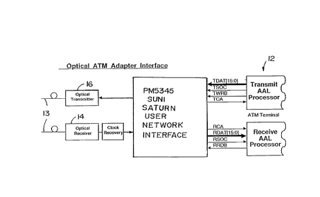
Referring to Figure 3, the user network
interface device l0 is fabricated as a monolithic
12 21~461~
integrated circuit that implements the SONET/SDH
processing and ATM mapping functions of a 155 Mbit/s STS-
3c user-network-interface. As shown, the device 10
couples a fibre optic line system 13 with an ATM terminal
12. On the line side an optical receiver 14 receives
light signals generated by a remote laser (not shown) and
converts them to electrical signals in SONET/SDH frames.
The frames are processed by the device 10 which then
transmits to the ATM Terminal 12 in the form of ATM
cells. It recovers the 155.52 Mbit/s clock signal from
the received frames and uses this clock to transmit to
the optical transmitter 16. ATM cells received by the
device 10 are processed and placed in transmitter 16.
Figure 4 shows a similar arrangement except that twisted
pairs 18 rather than fibre optic lines 13 are used.
Referring to Figure 5 there is shown the user
network interface device 10 which consists of a
parallel/serial transmit circuit 18 and a serial/parallel
receive circuit 20. Transmit circuit 18 transmits
SONET/SDH frames, via bit serial or byte serial signals
and receive circuit 20 receives such frames in bit serial
or byte serial format. Received bit serial signals are
converted by the user network interface device 10 to byte
serial format.
The output of the receive circuit 20 is coupled
to the input of a receive section overhead processor 22
which provides frame synchronization, de-scrambling,
section level alarm and performance monitoring. The
output of the receive section overhead processor 22 is
coupled to the input of a receive line overhead processor
26 which provides line level alarm and performance
monitoring. The output of the line processor 26 is
connected to the input of a receive path overhead
processor 28 which provides pointer interpretation,
extraction of path overhead, extraction of the
13 ~IZ461Q
_
synchronous payload envelope (SPE), and path level alarm
and performance monitoring.
Once SONET/SDN overhead processing is complete
the signals from the output of the receive path overhead
processor 28 are directed to the input of a receive ATM
cell processor 30. The ATM cell processor 30 performs
ATM cell delineation, provides cell filtering based on
idle/unassigned cell detection and HCS error detection,
and performs ATM cell payload descrambling. The output
of the receive ATM cell processor 30 couples to the input
of a 4 cell deep receive FIFO 32 which passes data
structures consisting of either 27 16-bit words, or 53 8-
bit words and is used to separate the STS-3c line timing
from the higher layer ATM system timing. The output of
the FIFO couples to the input of a drop side interface
34.
The drop side interface 34 can be accessed
through an external generic 16-bit or 8-bit wide
interface. When a cell is available in the receive FIFO
32, external circuitry is notified using the RCA output
signal 36 from the drop side interface 34. The external
circuitry may then read the cell from the buffer as a
word wide stream (along with a bit marking the first word
of the cell) at instantaneous rates of up to 25 MHz.
Similarly, external circuitry is notified,
using the TCA signal 38 from the drop side interface 34
when a cell may be written to the transmit FIFO 40 whose
input is coupled to the output of the drop side interface
34. The cell is written to the FIFO 40 as a word wide
stream (along with a bit marking the first word of the
cell) at instantaneous rates of up to 25 MHz.
The transmit FIFO 40 provides FIFO management
and the asynchronous interface between the device 10 and
the external environment. The transmit FIFO 40 can
14 ~12~6~
.,, ~
accommodate four cells. It provides for the separation
of the STS-3c line or physical layer timing from the ATM
layer timing.
The FIFO supports two data structures. The
first data structure consists of 27 16-bit words
comprising the 5 octet cell header and the 48 octet
payload (the Header Check Sequence {HCS} byte, along with
the header error insertion control byte, is passed in
this structure). The header error insertion control
allows the programmable insertion of one or more bit
errors in the HCS octet. The second data structure
consists of 53 8-bit words, comprising the 5 octet cell
header, and the 48 octet payload.
Management functions of the transmit FIFO 40
include filling the transmit FIFO 40, indicating when
cells are available to be written to the transmit FIFO
40, maintaining transmit FIFO read and write pointers,
and detecting a FIFO overrun condition. Upon detection
of an overrun condition, the FIFO 40 is automatically
reset. Up to four cells may be lost during the FIFO
reset operation. FIFO overruns are indicated through a
maskable interrupt and register bits. The synchronous
interface provided to an external device (not shown)
issues a TSOC signal to indicate to the Drop Side
Interface 34 and FIFO 40 that the first word of the
selected data structure is present on the TDAT bus. The
TWRB signal cycles from low to high as sent by the
external circuitry to tell the Interface 34 and FIFO 40
that the first word is coming. The external circuitry
is then notified by issuance of a TCA signal that a cell
may be written to the transmit FIFO 40 (cell available)
on the rising edge of TWRB (transmit write strobe) which
cycles at 25 MHz or lower. Once the cell is written to
the FIFO 40, the FIFO 40 changes from cell available to
cell unavailable status on write cell boundaries with
timing aligned to the transmit write strobe (TWRB).
129~D
The Transmit Cell Processor 42 coupled to the
output of the FIFO 40, inserts a cell offset indicator
byte H4 which indicates the offset in bytes between
itself, and the first cell boundary following the H4
byte. Processor 42 also provides rate adaptation via
idle/unassigned cell insertion and HCS generation and
insertion, and performs ATM cell scrambling. An idle or
unassigned cell is transmitted if a complete ATM cell has
not been written into the FIFO 40.
The Path Overhead Processor 44 has an input
coupled to the output of the Cell Processor 42. The
Transmit Path Overhead Processor (TPOP) 44 provides
transport frame alignment generation, pointer generation,
path overhead insertion, insertion of the synchronous
payload envelope, insertion of path level alarm signals
and a path bit interleaved parity calculation and
insertion for performance monitoring.
The input to the Line Overhead Processor 48 is
coupled to the output of the Path Overhead Processor 44.
The Transmit Line Overhead Processor (TLOP) provides line
level alarm insertion, and bit interleaved parity
insertion using even parity.
Finally, the Transmit Section Overhead
Processor (TSOP) 24 has an input coupled to the output of
the Transmit Line Overhead Processor 4~. The TSOP
provides frame pattern insertion, scrambling, section
level alarm signal insertion and bit interleaved parity
insertion.
To the Transmit Line Overhead Processor 48
there is connected a Transmit Line Overhead Insert Port
which optionally inserts 81 bytes of transmit
transport overhead from a data stream received serially
at 5.184 Mbit/s from external sources. A Path Overhead
~ 16 212~610
Insert Port 46 is coupled to the Path Overhead Processor
44 and provides a bit serial path overhead interface to
the Transmit Path Overhead Processor (TPOP) 44. Any, or
all of the path overhead bytes may be sourced from, or
modified by the bit serial path overhead stream.
Coupled to the output of the Line Overhead
Processor 48 and to the input of the transmit circuit 18
is the section overhead processor 24 which provides frame
pattern insertion, descrambling, section level alarm and
performance monitoring. The output of the Section
Overhead Processor 24 is also coupled to the Line Side
Interface 52.
Cell Rate Decoupling
ATM cells may be passed to/from the drop line
interface 34 using one of two defined data structures,
namely, a 9-bit structure consisting of a start of a cell
indication, and an 8-bit wide word as shown in Figure 6.
Here H1 to H5 are pointer bytes and a cell boundary
offset byte. Words 6 to 53 contain the payload bytes.
Figure 7 shows the data structure for a 17-bit
structure consisting of a start of cell indication, and a
16-bit wide word. Here the header includes a header
check sequence octet.
Because the ATM cells are asynchronous whereas
the SONET/SDH frames are sent at 155.52 Mbit/s, in order
to go from one transmission mode to the other, it is
necessary to decouple the timing for the data in one mode
from that in the other.
In going from ATM to SONET/SDH, the ATM cells
arrive at the transmit side of the Drop Side Interface 34
at irregular intervals. Consequently, a buffer must be
used to temporarily store bytes so that they can then be
2~2~
17
"_
read out from the buffer at a rate which is synchronized
to the desired bit rate for SONET/SDH of 155.52 Mbit/s.
In this case, the buffer is a four cell
transmit FIFO 40. ATM cells are stored in the transmit
FIFO 40 after passing through the Drop Side Interface 34.
The Drop Side Interface 34 first sends out a TCA signal
to notify the external circuitry that a cell may be
written to the transmit FIFO 40. To accomplish this, as
shown in the timing diagram of Figure 8, the TCA output
transitions from 0 to 1 when the transmit FIFO 40
contains one empty cell. The transmit write strobe
(TWRB) then cycles at 25 MHz or lower and data is then
sampled on the rising edge of the TWRB cycles until a
complete cell has been transferred. The process is then
repeated.
Going from SONET/SDH to ATM, ATM cell
boundaries must be located in the synchronous payload
envelope of each frame, verified and the cells placed in
the receive FIFO 32. These cells are then read out of
the receive FIFO 32 to external ATM circuitry in response
to an active receive read strobe signal from this
external circuitry.
Figure 8 shows the timing diagram for the
receive FIFO 32. The RCA output transitions from 0 to l
when a cell is available in the FIFO 32. Once read
strobe signal RRDB begins to cycle, words are transmitted
on each cycle of RRDB for at most 100 ns to avoid
overrunning the FIFO 32. RSOC is high during the first
word of the 27 word data structure.
Because in SONET or SDH a continuous stream of
cells is transmitted in sequence, whereas in ATM the cell
stream is non-continuous, transforming a non-continuous
cell stream into a continuous one requires inserting idle
or unassigned cells (cells containing no payload) during
18 al 2A ~1 0
'_
idle periods in the assigned cell stream. Consequently,
in going from SONET to ATM it is necessary to recognize
and discard these idle cells. This is done by simply
testing the header pattern to determine if it is in the
format for an unassigned cell. In the present case the
first four octets or bytes in the header will each be 00H
if the cell is idle or unassigned.
ATM Cell Delineation
Cell delineation is the process of framing to
ATM cell boundaries using the header check sequence (HCS)
field found in the cell header. The HCS is a cyclic
redundancy check calculation over the first 4 octets of
the ATM cell header (see Figure l). When performing
delineation, correct HCS calculations are assumed to
indicate cell boundaries. Cells must be byte aligned
before insertion in the synchronous payload envelope.
Thus, a cell delineation algorithm can search the 53
possible cell boundary candidates one at a time to
determine a valid cell boundary location. While
searching for the cell boundary location, the cell
delineation circuit is in the HUNT state 60 shown in
Figure 9. When a correct HCS is found, a cell
delineation state machine (not shown) locks on the
particular cell boundary and enters the PRESYNC state 62.
This state 62 validates the cell boundary location. If
the cell boundary is invalid then an incorrect HCS will
be received within the next DELTA cells, at which a
transition back to the HUNT state 60 is executed. DELTA
is a value to be selected. If no HCS errors are detected
in this PRESYNC period 62 then the SYNC state 64 is
entered. While in the SYNC state 64, synchronization is
maintained until a ALPHA consecutive incorrect HCS
patterns are detected, where ALPHA is a value to be
selected. In such an event a transition is made back to
the HUNT state 60 is executed. The values of ALPHA and
DELTA determine the robustness of the delineation method.
ALPHA determines the robustness against false
l9
~12A6~ ~
misalignments due to bit errors. DELTA determines the
robustness against false delineation in the
synchronization process. ALPHA is chosen to be 7 and
DELTA is chosen to be 6. These values result in a
maximum average time to delineate of 31 microseconds.
Cells are filtered based on HCS errors and/or a
cell header pattern. Cell filtering is optional and is
enabled through the registers of the Receive ATM cell
Processor 30 (RACP). Cells are passed to the receive
FIFO 32 while the cell delineation state machine is in
the SYNC state 64 as described above. When both
filtering and HCS checking are enabled, cells are dropped
if uncorrectable HCS errors are detected, or if the
corrected header contents match the pattern contained in
the 'Match Header Pattern' and 'Match Header Mask'
registers. Idle or unassigned cell filtering is
accomplished by writing the appropriate cell header
pattern into the 'Match Header Pattern' and 'Match Header
Mask' registers. Idle/Unassigned cells are assumed to
contain the all zeros pattern in the VCI and VPI fields.
The 'Match Header Pattern' and 'Match Header Mask'
registers allow filtering control over the contents of
the GFC, PTI, and CLP fields of the header. The HCS is a
cyclical redundancy check calculation over the first 4
octets of the ATM cell header. The RACP block verifies
the received HCS using the polynomial, x8 + x2 + x + 1.
The coset polynomial, x6 + x4 + x2 + 1 is added (modulo
2) to the received HCS octet before comparison with the
calculated result. While the cell delineation state
machine (referred to above) is in the SYNC state 64, the
HCS verification circuit implements the state diagram
shown in Figure 7. In normal operation the HCS
verification state machine remains in the 'Correction
Mode' state 64. Incoming cells containing no HCS errors
are passed to the receive FIFO 32 (of Fig 5). Incoming
single bit errors are corrected, and the resulting cell
is passed to the FIFO 32. Upon detection of a single bit
_ 20 2124610
error or a multi bit error, the state machine transitions
to the 'Detection Mode' state 68. In this state, the
detection of any HCS error causes the corresponding cell
to be dropped. Cells containing an error-free HCS are
passed, and the state machine transitions back to the
'Correction Mode' state 66.
Overhead Access Port
The user network interface device 10 has
transmit and receive overhead access ports 51 and 53,
respectively. The receive overhead access port 53
includes a receive transport overhead extract port 54 and
a receive path overhead extract port 56. The transport
overhead extract port 54 extracts the 81 bytes of receive
transport overhead and serializes them at 5.184 Mbits/s
for optional external processing. A receive transport
overhead frame position (RTOHFP) signal is used to locate
the individual receive transport overhead bits in the
transport overhead data stream. To this end the RTOHFP
signal is logic one while bit 1 (the most significant
bit) of the first framing byte (Al) is present in the
receive transport overhead data stream.
The path overhead extract port 56 uses timing
information from the synchronous payload envelope (SPE)
block to extract, serialize and output the path overhead
bytes on output receive path overhead data. The receive
path overhead clock (RPOHCLK) is nominally a 576 kHz
clock which provides timing to process the extracted
receive path overhead. RPOHCLK is used to identify the
most significant bit of the path trace byte (Jl) on the
receive path overhead data.
The transmit transport overhead insert port 50
optionally inserts the 81 bytes of transmit transport
overhead from a data stream of transmit transport
overhead data received serially at 5.184 Mbit/s. The
transport overhead bytes include Al, A2, Cl, El, Fl,
21 212~GlQ
._
D1-D3, K1, K2, D4-D12, Z1, Z2, and E2 and error masks B1,
B2, H1, and H2. The transmit transport overhead frame
position (TTOHFP) signal may be used to locate the
individual transport overhead bits in the transport
overhead data stream. TTOHFP is logic one while bit 1
(the most significant bit) of the first framing byte (A1)
is expected in the transmit transport overhead data
stream. An enable signal TTOHEN, is provided to allow
per byte control of such optional transport overhead
insertion.
The state of the TTOHEN input determines
whether the data sampled on the transmit transport
overhead data stream (TTOH), or the default overhead byte
values shown in Figure 8 are inserted in the STS-3c
stream. For example, a high level on TTOHEN during the
section user channel (F1) bit positions causes the eight
values shifted in on TTOH to be inserted in the F1 byte
position in the STS-3c stream. A low level on TTOHEN
during the section sure channel bit positions causes the
default value (0x00) to be inserted in the STS-3c stream.
Other combinations are also possible.
During the H1, H2, B1 and B2 byte positions in
the TTOH stream, a high level on TTOHEN enables an error
insertion mask. While the error mask is enabled, a high
level on input TTOH causes the corresponding bit in the
H1, H2, B1 or B2 byte to be inverted. A low level on TTOH
causes the corresponding bit in the B1 or B2 byte to pass
through the device uncorrupted.
The path overhead insert port 46 provides a bit
serial path overhead interface to the transport path
overhead processor 44. Any or all of the path overhead
bytes may be sourced from, or modified by the bit serial
path overhead stream, TPOH. The individual bits of each
path overhead byte are shifted in using the transport
path overhead clock output, TPOHCLK. The transport path
22 ~124~
.,
overhead frame position signal, TPOHFP, output is
provided to identify when the most significant bit of the
path trace byte is expected on TPOH. The state of the
transport path overhead enable, TPOHEN, input, together
with an internal register, determines whether the data
sampled on TPOH, or the default path overhead byte values
are inserted in the STS-3c stream. For example, a high
level on TPOHEN during the path trace (Jl) bit positions
causes the eight values shifted in on TPOH to be inserted
in the Jl byte position in the STS-3c stream. A low
level on TPOHEN during the path trace bit positions
causes the default value (0x00) as shown in Figure 9 to
be inserted in the STS-3c stream. Other combinations are
also possible.
During the B3 and H4 byte positions in the TPOH
stream, a high level on TPOHEN enables an error insertion
mask. While the error mask is enabled, a high level on
input TPOH causes the corresponding bit in the B3 or H4
byte to be inverted. A low level on TPOH causes the
corresponding bit in the B3 or H4 byte to pass through
the TPOP uncorrupted.
Referring to Figure 11, there is shown a
configuration in which four of the devices are used in
parallel with four corresponding STS-3/STM-l ATM streams
to produce four synchronous SONET streams which are then
multiplexed into a single STS-12/STM-4 stream at 622
Mbit/s.
Accordingly, while this invention has been
described with reference to illustrative embodiments,
this description is not intended to be construed in a
limiting sense. Various modifications of the
illustrative embodiments, as well as other embodiments of
the invention, will be apparent to persons skilled in the
art upon reference to this description. It is therefore
contemplated that the appended claims will cover any such
23 ~12g 61~
modification or embodiments as fall within the true scope
of the invention.