Note: Descriptions are shown in the official language in which they were submitted.
1
Title: IGNITION SYSTEM USING MULTIPLE GATED SWITCHES
WITH VARTABLE DISCHARGE ENERGY LEVELS AND RATES
BACKGROUND OF THE INVENTION
The invention relates generally to ignition systems.
More particularly, the invention relates to ignition systems
that use gated switches for controlling energy discharge to a
plurality of igniters.
Conventional ignition systems typically include one or
more igniters through which energy is discharged from an
energy storage device such as a capacitor. The discharge is
characterized by a high currentJvoltage spark or plasma that
occurs due to high voltage breakdown across the igniter gap,
including air gap and semiconductor gap igniter plugs.
A conventional ignition system for an internal combustion
engine, such as, for example, a gas turbine aircraft engine,
includes a charging circuit, a storage capacitor, a discharge
circuit and at least one igniter plug located in the
combustion chamber. The discharge circuit includes a
switching device connected in series between the capacitor and
the plug. For many years, such ignition systems have used
spark gaps as the switching device to isolate the storage
capacitor from the plug. When the voltage on the capacitor
reaches the spark gap break over voltage, the capacitor
discharges through the plug and a spark is produced. More
recently, solid state switches such as SCR, G~0 and MCT
devices have been investigated.
It is generally known that energy levels from multiple
storage means can be combined to increase discharge energy
through a single igniter. It is also known that a single
energy storage source can be multiplexed to produce sparks in
a plurality of igniters, such as shown in U.S. Patent No.
3,880,132 issued to Whatley. However, this arrangement is
unsuitable for applications such as gas turbine engine
ignition systems because the use of a single pulse forming
(wave shaping) network can overstress solid state gated
switches. In another arrangement, such as shown in U.S.
~~~~~J~
2
Patent No. 3,605,75.4 issuEd to Hardin, a single capacitor is
used to produce sparks in multiple plugs including the use of
separate pulse shaping networks to reduce stress on the
switches, such as might be used in a spark distribution system
that fires each plug at a rate proportional to engine speed.
However, this system is unsuitable for aerospace applications
wherein discharge energy and spark rates need to be controlled
based on factors other than engine speed, such as igniter
wear, temperature, fuel mix, and turbulence, for example.
The objectives exist, therefore, for an ignition or spark
discharge system that can produce different energy level
discharges to selectable igniters, as well as at different
spark rates. Particularly needed is such a system that can be
adapted for use with gas turbine engines, such as used in
aircraft applications.
SiJNa~fARY OF THE INVENTION
Accordingly, the invention contemplates in one embodiment
an ignition system for a gas turbine engine comprising: a
plurality of igniters, an energy storage capacitance, a
charging circuit for charging the capacitance, a plurality of
gated switches, with at least one switch connected between
each igniter and the capacitance, and control means for
discharging respective amounts of energy from the capacitance
to each respective igniter at respective spark rates.
These and other aspects and advantages of the present
invention will be readily understood and appreciated by those
skilled in the art from the following detailed description of
the preferred embodiments with the best mode contemplated for
practicing the invention in view of the accompanying drawings.
BRIEF DESCRIPTION OF THE DRAWINGS
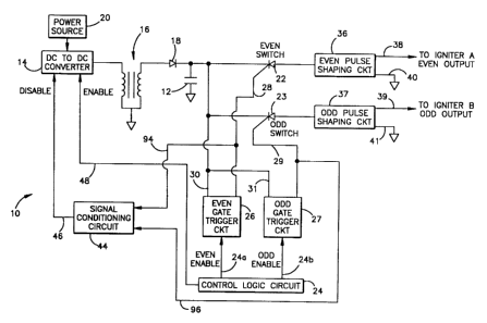
Fig. 1 is an electrical schematic in primarily functional
block diagram form of an ignition system and exciter circuit
according to the present invention;
Fig. 2 is a more detailed schematic of one embodiment of
the invention as shown in Fig. 1; and
~~~~~93~
3
Fig. 3 is a more detailed schematic of a control circuit
that can be used in the embodiments of Figs. 1 and 2, and a
simplified timing diagram showing operation of the control
circuit.
DETAINED DESCRIPTTON OF THE INVENTION
With reference to Fig. 1, a schematic functional block
diagram of an embodiment of an exciter circuit and ignition
system in accordance with the invention is generally
designated by the numeral 10. Although an embodiment of the
invention is described herein with respect to a specific form
or configuration of an exciter circuit in combination with a
specific type of ignition system, this description is intended
to be exemplary and should not be construed in a limiting
sense. Those skilled in the art will readily appreciate that
the advantages and benefits of the invention can be realized
with many different types of ignition systems and exciter
circuit designs including, but not limited to, unidirectional
discharge, oscillatory discharge, AC and/or DC charging
systems, capacitive and other discharge configurations, spark
gap and solid-state switching circuits, high tension.and low
tension discharge circuits, and so on, to name just a few of
the many different ignition systems and exciter circuit
configurations. Furthermore, the invention can be used in
combination with ignition systems for many different types of
engines, although the description herein is with specific
reference to use with a gas turbine engine ignition system
particularly well-suited for use in aerospace applications.
An exemplary exciter circuit is shown in Fig. 1, and
includes a main storage capacitance or capacitor 12 that is
connected to a charging circuit 14 which receives input power
from a power source 20, such as a DC voltage supply from the
engine power plant (in the case of an AC circuit, for example,
the source 20 could be an output from the engine alternator.)
The charging circuit 14 can be an AC or DC charging source
depending on the particular requirements for each application.
The charging circuit 14 design can be conventional, such as a
''~~~i)~~
4
DC converter as in the drawings, or a continuous AC supply
circuit, for example.
The converter 14 includes a power transformer 16 that
produces an AC charging current in its secondary, and the
current is half-wave rectified by a diode 18 connected to the
capacitor 12. Full wave rectification could also be used if
needed for a particular application. '
The capacitor 12 is also connected to one side of a
pair of switching mechanisms or devices 22,23. The switching
devices can be realized many different ways such as in the
form of a spark gap, a gated spark gap, gated solid state
switches such as SCR, GTO or MCT devices, either single or
cascaded, and so on. In the embodiment shown herein, single
SCRs are used for each switch. One of the SCRs 22 is
designated as the "even" switch 22 and the other SCR is
designated as the "odd" switch 23, however, these designations
are arbitrary and only used for convenience and ease of
explanation. According to an important aspect of the
invention, the capacitor 12 can be sequentially discharged
through a plurality of igniters using different discharge
energies at different spark rates. In this embodiment, we
show a two channel design that implements two discharge energy
levels and spark rates. Therefore, one channel will be
referred to as the even channel and the other the odd channel
in order to distinguish the two.
The ignition system exciter circuit further includes a
control logic circuit 24 that enables and disables the
discharge channels at the appropriate times by providing
control signals to respective trigger circuits 26,27 via lines
24a and 24b. The trigger circuits 26,27 respectively produce
gate trigger outputs on lines 28,29 to cause the corresponding
SCR to turn on at the appropriate time. The trigger circuits
26,27 also respectively receive as an input (on lines 30,31)
the voltage level stored on the capacitor 12. In the
particular embodiment herein, an SCR is triggered on as soon
as the capacitor 12 is charged to the appropriate level for
the respective igniter. Those skilled in the art will readily
- h
recognize this as a "wait and charge" timing arrangement, but
other timing sequences such as °'charge and wait°', for example,
could easily be used with the invention. For example, the
control circuit can trigger the switch closed after the
5 capacitor reaches a predetermined charge level, or the circuit
can trigger the switch at a predetermined rate based on the
desired spark rate.
Each switching device 22,23 is also connected to a
corresponding pulse shaping and output circuit 36,37. The
l0 output circuits 36,37 configurations can be selected based on
the particular application of the ignition system. In this
exemplary circuit, the output circuits include free wheeling
diodes which force the discharge current to be unidirectional,
such as is typically required for solid state switching
mechanisms. The diode can be omitted to produce oscillatory
discharge circuits such as are common with spark gap switching
devices. An exemplary embodiment of a high tension output
circuit is illustrated in Fig. 2 and is well known to those
skilled in the art. This is but one example, however, and its
description herein should not be construed as a limitation of
the invention. Other pulse shaping circuits are well known,
such as current and/or voltage step-up circuits and
distributed or multiplexed output controls, just to name a few
examples.
Each pulse shaping circuit output is connected to an
igniter (not shown) by a conductor, such as a high
voltage/current cable lead 38,39 and a return lead 40,41.
Examples of igniters that can be used include airgap, semi-
conductor, but this list is not exhaustive and should not be
construed in a limiting sense as to the present invention.
A signal conditioning circuit 44 has inputs connected to
the gate trigger control signals from the trigger circuits
26,27. The conditioning circuit 44 monitors these signals,
and when a trigger signal is detected, the circuit 44 sends a
disable control signal on line 46 to the converter 14, thereby
turning the converter off during the capacitor 12 discharge
~l~~f~~~
6
period. The converter 14 is turned back on by an enable
signal on line 4$ produced by the control circuit 24.
rn operation, each switching mechanism is triggered on
in a controlled sequence after the capacitor is fully charged,
and the capacitor voltage is impressed across the
corresponding igniter gap for the igniter in sequence.
Assuming the voltage exceeds the breakover voltage of the gap,
a plasma or similar conductive path jumps the gap and the
capacitor quickly discharges with current rising rapidly as
l0 represented by the simplified graph 26 in the drawing.
Typical discharge times are on the order of tens of
microseconds. Tn accordance with the invention, although the
switches 22,23 are sequentially triggered, the control circuit
24 operates with the trigger circuits 26,27 so that each
switch can be triggered at a different rate to produce
different spark rates for each igniter, if desired. The
control circuits also operate to allow different energy levels
to be discharged from the same capacitance 12 through the
different igniters. Of course, the designer may only want
different spark rates but the same discharge energy levels for
each igniter, or conversely may want the same spark rate for
each igniter but different energy levels. All these different
combinations as well as others can be .realized with the
present invention with simple modifications to the control
circuit. For example, different discharge energies can be
realized by adjusting threshold levels on a comparator used to
sense the charge stored on the capacitor 12. Different spark
rates can easily be implemented by simply changing the timing
clocks for the control signals used to trigger the switches
and control the converter 14. These design alternatives will
be apparent to those skilled in the art from the following
description of a detailed embodiment (Fig. 2) of the circuit
shown in Fig. 1.
With reference then to Fig. 2, we show in greater detail
an embodiment of the invention, such as may be used, for
example, to realize the circuit shown in Fig. 1 (wherein like
components are given like reference numerals.) The charging
7
circuit 14 receives input energy V~' and V° from a power
source. The charging circuit can be a simple DC chopper
circuit that includes a switch that is periodically activated
to pulse current through the primary of the power transformer
16. The rectifying diode 18 provides unidirectional half-wave
charging current to the main storage capacitance 12.
A tertiary winding 52 produces an ac voltage that 'is
rectified by a diode 54 to charge a capacitor 56. The DC
voltage that appears across the capacitor is used as a DC
supply for the various control devices in the circuit 20. A
current regulator 58 and zener diode 60 can be used to provide
a stable DC supply.
The capacitor 12 is connected to the switching devices
22,23. Shunting diodes 62,64 are connected across the anode
and cathode of each SCR to reduce the risk of damage to the
solid state switches from reverse currents. The even channel
switch 22 is connected to a high voltage output pulse shaping
circuit 36 that includes a step-up transformer 66 and a free
wheeling diode 68. The odd channel switch. 23 is similarly
connected to a step-up transformer 70 and free wheeling diode
72. The step-up transformers allow a higher initial. voltage
to appear across the plug gaps than can be stored on the
capacitor 12 when a single device SCR is used. This is
because of the device limitations as to reverse blocking
voltage and breakdown. Of course, cascaded switches can be
used to increase the voltage stored on the capacitor 12.
Also, the different discharge channels can use different pulse
shaping circuits, and in fact one could be unidirectional (by
use of the free wheeling diode) while the other could be
oscillatory (for example with the use of a spark gap. ) It
should further be noted that the invention is not limited to
only a two discharge channel design, but can be implemented in
a larger plurality of channels with simple appropriate changes
to the control and trigger logic circuits as will be apparent
to those skilled in the art.
Discharge resistors 74a and 74b provide a discharge path
in the event that an igniter does not break over to produce a
J
8
spark. The transformers 66,70, are connected, of course, to
their respective igniters (not shown) via the high tension
leads 38,39 and returns 40,41.
Each SCR 22,23 has a gate terminal that is connected to
a trigger circuit 26,27. The circuits 26,27 are identical in
design (though they control different operating discharge
rates and energy levels for each channel), therefore, the
circuitry will be described for one channel only.
The trigger circuit 26 includes a comparator device 80,
such as part no. ICM 7555 available from Harris
Semiconductors. An input pin 7 of the comparator is connected
to a resistor divider that includes series resistors 82 and
84. The resistor divider is connected as at node 86 to the
capacitor 12. Therefore, the comparator can monitor the
charge level on the capacitor. The comparator device 80 has
an adjustable internal threshold which can be selected, along
with the resistor divider components, to trigger the
comparator at any desired charge level on the capacitor.
Also, the sense node 88 could be connected to an external
circuit, such as an on board controller on an aircraft, to
dynamically change the discharge energy level by adjusting the
resistor divider sensitivity level (or the user could simply
connect an external bias circuit to the. sense node 88 to
customize the channel discharge energy level as desired.)
when the capacitor is charged to the threshold level set
by the designer, the comparator device 80 produces a short
pulse at output pin 5 that turns on a switching FET transistor
90 which in turn pulses a PNP transistor 92. The PNP
transistor thus applies a gate drive pulse signal to the SCR
22 that causes the SCR to conduct, essentially short
circuiting the capacitor 12 across its associated igniter via
the step-up transformer 66. After the capacitor 12 discharges
below the sustaining voltage of the SCR 22, the SCR 22 returns
to its blocking state and the capacitor 12 can be charged for
the next cycle. The foregoing description of the circuit 26
is sufficient for purposes of understanding and practicing the
invention herein; however, if interested, a more detailed
CA 02128036 2002-06-12
9
description of the circuit is set forth in U.S. Patent No. 5,488,536.
The signal conditioning circuit 4~ detects the gate
trigger pulse from the PNP transistor 92 via line 94 (and also
monitors the occurrence of a trigger signal in the odd channel
via line 96). The conditioning circuit 44 can be a simple OR
circuit and pulse generator such as a one-shot that
appropriately isolates the trigger circuitry from the
converter 14. The conditioning circuit produces a converter
disable signal on line 46. This disable signal temporarily
l0 stops operation of the converter (thereby preventing charging
current to the capacitor while the SCRs are in conduction)
until the capacitor has discharged and an enable signal is
received from the control logic 24 (note that in Fig. 2 the
control logic is shown as a single funcaional block With the
converter although this arrangement is optional to the
designer) to restart the converter. The disable signal is
processed by the converter 14 in accordance with the converter
design. As an example, the disable signal can be used to
interrupt the base drive to the chopper transistor 50.
The control logic circuit 24 produces a control signal on
line 98 that enables the even channel. The odd channel enable
signal is provided on line 100. The channel enable signal for
the even channel controls operation of an enable FET switch
102. When the FET switch 102 is turned on, the comparator
device 80 is disabled and therefore cannot trigger the even
channel switching device 22 into conduction. Similarly, an
odd channel FET switch 104 is used to enable and disable the
odd channel comparator.
With reference next to Fig. 3, we show an embodiment of
a control logic circuit suitable for use with the invention,
as well as a representative timing diagram for a two channel
design. The control logic is realized in the form of a
/....iy
counter 110 that receives a clock drive 112 from a suitable
clock source (not shown). A series of logic gates Such as OR
gates 114 are used to decode the counter outputs to produce
the desired even and odd channel enable timing signals. In
5 this case, the even signal has a pulse rate that is twice the
frequenc~~ as the od channel. Other timing scenarios can be
used of course and implemented in many different ways.
Further note that an additional OR gate 116 is used to produce
a converter 14 enable signal. In the example embodiment
10 herein, the rising edge of either the even or odd enable
signal, such as at 118, causes the converter to charge the
capacitor 12, provided that there is not a disable signal
appearing on the control line 46 (which would indicate that
the capacitor 12 is still discharging through a conducting
SCR.) The signal conditioning circuit produces a disable
signal pulse that lasts for a time period that is sufficient
to allow the capacitor 12 to discharge and the SCR device to
recover and fully turn off. Therefore, this disable pulse can
be rather short in duration. Other sensing circuits could be
added to affirmatively detect when the SCR device turn off, if
desired.
Operation of the described embodiment of the invention is
as follows. Assuming that the capacitor 12 is discharged and
the switches 22,23 are off (non-conducting), the converter 14
is enabled by the control circuit 24 when either or both of
the even/odd channel enable signals is high. The capacitor 12
quickly charges, typically on the order of tens of
milliseconds. Whichever channel is enabled (even or odd) for
the current discharge cycle, the corresponding comparator
monitors the capacitor charge level. When the capacitor is
charged to the preselected discharge energy level, the
comparator pulses the corresponding switch into conduction and
the capacitor discharges through the associated igniter.
During this discharge period the signal conditioning circuit
disables the converter 14. The capacitor 12 discharge time is
very short and as soon as the switching device 22,23 turns
off, the capacitor can be charged. The charging cycle,
~.-_,,
11
however, does not begin until the next enable signal from the
control logic is received, which signal also functions to
select which channel will be the discharge channel for the
next cycle.
Thus, an ignition system and exciter circuit are provided
that can be used to produce individual spark rates for a
plurality of igniters, as well as to permit discharge 'of
individual energy levels through the igniters from a single
energy storage device. This significantly increases the
l0 flexibility and utility of the ignition system and exciter
circuit for many different applications, particularly in the
aerospace industry.
While the invention has been shown and described with
respect to specific embodiments thereof, this i's for the
purpose of illustration rather than limitation, and other
variations and modifications of the specific embodiments
herein shown and described will be apparent to those skilled
in the art within the intended spirit and scope of the
invention as set forth in the appended claims.