Note: Descriptions are shown in the official language in which they were submitted.
Si'FCIFICATIQi~T '~ ~, ~ ~ ~ 3 ~ ~- 3 B~CT-
Antenna Devices
Technical field
This invention relates to small printed antenna devices which resonate at two
resonant frequencies. This invention is particularly suitable for utilization
as a built-in
antenna for a small portable radio unit.
Bacl~ground technology
Known examples of antenna devices which resonate at two resonant frequencies
include the planar inverted-F antenna disclosed in Japanese Pat. Pub. No. 61-
41205
(Pat. Appl. No.59-162690) and microstrip antennas presented in "Handbook of
Microstrip Antennas" by J.R. James and P.S. Hall.
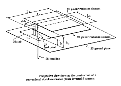
Figure 1 is a perspective view showing the construction of the planar inverted-
F antenna disclosed in the above-mentioned application. This prior art example
has
a first planar radiation element 21 and a second planar radiation element 22,
and these
are arranged parallel to ground plane 23. The two planar radiation elements 21
and
22 are mutually connected by stub 24, and first planar radiation element 21
and
ground plane 23 are connected by stub 25. The non-grounded conductor of feed
line
26 is connected to planar radiation element 21 at contact point 27, while the
grounded
conductor of feed line 26 is connected to ground plane 23. The dimensions
LlxL2 of
planar radiation element 21 differ from the dimensions L3xL4 of planar
radiation
element 22, which means that they resonate at different resonant frequencies
to give
a double resonance. In other words, the planar inverted-F antenna constituted
by
planar radiation element 21 and the planar inverted-F antenna earned on top of
it
resonate independently, and are fed by a single feed line 26.
Figures 2-4 show examples of three cross-sectional structures of microstrip
antennas. In these antennas, first planar radiation element 31 and second
planar
radiation element 32 are again arranged parallel to ground plane 33, but two
feed lines
34 and 35 are connected to these (in the example given in Figure 4, only feed
line 34
is connected). In these cases as well, the size and structure of the two
planar radiation
elements 31 and 32 are different, and they resonate independently to give a
double
resonance.
Consequently, the thickness h2 of a conventional double-resonance planar
inverted-F antenna has to be approximately twice the thickness h~ of a single
planar
inverted-F antenna. The disadvantage of the prior art has therefore been that
an
antenna has to have a larger capacity and a more complicated structure in
order to
obtain double resonance characteristics.
~12~~.3~~
Conventional double-resonance microstrip antennas have the advantage that the
two frequencies can be selected relatively freely, but because structurally
they are
basically two antennas on top of one another, the disadvantage has again been
that the
antenna volume is larger and its structure more complicated. A further
disadvantage
of multiresonant microstrip antennas of the basic type has been their lack of
resonance
below the f~'st ande resonant frequency.
The purpose of this invention is to solve such problems and to provide an
antenna device which, although small and simple in construction, has double
resonance
characteristics.
Disclosure of the invention
The antenna device offered by this invention is characterised in that, in an
antenna device which has a conductive ground plane, a conductive planar
radiation
element arranged approximately parallel to this ground plane with an
intermediary
insulator, and a feed line with a grounded conductor which is connected to the
ground
plane and a non-grounded conductor which is connected to the planar radiation
element: a parasitic line is connected to another contact point at a distance
from the
contact point of the feed line, said parasitic line having a grounded
conductor
connected to the ground plane and a non-grounded conductor connected to the
planar
radiation element. Given this constitution, the parasitic line constitutes a
stub and the
antenna device can exhibit double resonance characteristics.
When a line with open ends is used as the aforementioned parasitic line, if A
is the resonant wavelength when the points of contact of this parasitic line
with the
ground plane and the planar radiation element are short-circuited, the
electrical length
of this parasitic line is made:
(1/4 + m/2) ~,
where m is an integer equal to or greater than 0.
It is also feasible to provide resonant wavelength tuning slits in edges of
the
planar radiation element, and to tune the lower of the two resonant
frequencies.
It is also feasible to provide a plurality of parasitic lines. In particular,
a
preferred construction is as follows. Namely, the planar radiation element has
a shape
such that at least two sides are mutually opposed, and there are provided a
first
parasitic line with a contact point which is approximately the centre of one
of these
two sides, and second and third parasitic lines with contact points which are
respectively the ends of the other of these two sides. If A is the resonant
wavelength
when the planar radiation element and the ground plane are connected by a
short-
circuited line instead of by the first parasitic line, and when there are no
second and
third parasitic lines, the respective electrical lengths of the first
parasitic line and the
21291r~~
second and third parasitic lines are set so as to be approximately equal to
the value
given by:
(1/4 + m/2) x ~,
where m, is an integer which is equal to or greater than 0 and which is
established
independently for each parasitic line. The terminal of the first parasitic
line
that is distant from the planar radiation element and the ground plane is
opened,
while the terminals of the second and third parasitic lines that are distant
from the planar radiation element and the ground plane are short-circuited.
Given this construction, at the lower resonant frequency the first parasitic
line
achieves a short stub between the planar radiation element and the ground
plane, while the second and third parasitic lines perform open , ' antenna
device
-circ x.
will therefore operate as a planar inverted-F antenna. At the ~iigher resonant
frequency, the first parasitic line achieves open 1e second and third
parasitic
=circu' t~
lines perform short stubs between the planar radiation element and the ground
plane, so that this antenna device will operate as a quarter-wavelength
microstrip
antenna. In other words, double resonance characteristics are obtained. Under
these
circumstances, one of the two resonant frequencies will be approximately twice
that
of the other.
When this antenna device operates as a quarter-wavelength microstrip antenna,
the resonant frequency is determined by the second and ~uifd parasitic lines
becoming
short-circuited lines. Under these circumstances, fine tuning of the resonant
frequency
will be possible if the first parasitic line is used as an additional
impedance. When
the device operates as a planar inverted-F antenna, the resonant frequency is
determined by the first parasitic line becoming a short stub, . . so that fine
tuning of the resonant frequency will be possible by using the second and
third
parasitic lines as additional impedances.
Embodiments of this invention will now be explained with reference to the
accompanying drawings.
Brief explanation of the drawings
Figure I is a perspective view showing the construction of a conventional
double-resonance planar inverted-F antenna.
Figure 2 shows the cross-sectional structure of a conventional double-
resonance
microstrip antenna.
Figure 3 shows the cross-sectional structure of a conventional double-
resonance
microstrip antenna.
2~.~J1~9
r.
Figure 4 shows the cross-sectional structure of a conventional double-
resonance
microstrip antenna.
Figure 5 is a perspective view showing the constitution of a first embodiment
of this invention.
Figure 6 gives an example of the results of measurement of the return loss
characteristics of the first embodiment.
Figure 7 shows the measured return loss characteristics when the parasitic
line
is not connected.
Figure 8 shows the measured return loss characteristics when the parasitic
line
is changed short-circuited metal line.
f or
Figure 9 shows the current distribution on the planar radiation element and
within the parasitic line at the higher resonant frequency fH.
Figure 10 shows the current distribution on the planar radiation element and
within the parasitic line at the lower resonant frequency ft.
Figure 11 is a perspective view showing the constitution of a second
embodiment of this invention.
Figure 12 is a perspective view showing the construction of an antenna device
according to a third embodiment of this invention.
Figure 13 gives an example of the results of measurement of the return loss
characteristics of the third embodiment.
Figure 14 shows the measured return loss characteristics when, as a
comparison, the first parasitic line is not connected.
Figure 15 shows the measured return lass characteristics when, as a
comparison, the second and third parasitic lines are not connected.
Figure 16 serves to explain the operating principles, showing the current
distributions at the higher resonant frequency fly.
Figure 17 serves to explain the operating principles, showing the current
distributions at the lower resonant frequency f~.
Figure 18 is a perspective view of an antenna device according to the third
embodiment fitted in an enclosure.
Figure 19 shows results of measurements of the radiation pattern when
f=1.48 GHz.
Figure 20 shows the results of measurements of the radiation pattern when
f=0.82 GHz.
-5- 212~1~9
Optimum configurations for embodying the invention
Figure 5 is a perspective view showing the constitution of a first embodiment
of this invention. This embodiment has conductive ground plane 2, conductive
planar
radiation element 1 arranged approximately parallel to this ground plane 2
with an
intermediary insulator, and feed line 3 with grounded conductor 3a connected
to
ground plane 2 and non-grounded conductor 3b connected to contact point 3c of
planar
radiation element 1. Parasitic line 4 is connected to a separate contact point
4c at a
distance from contact point 3c of feed line 3, said parasitic line 4 having
grounded
conductor 4a connected to ground plane 2 and non-grounded conductor 4b
connected
to planar radiation element 1.
Transmitter or receiver 6 is connected to feed line 3, and terminals of
parasitic
line 4 is open. If a is the resonant wavelength when the points of contact of
parasitic
line 4 with ground plane 2 and planar radiation element 1 are short-circuited,
the
electrical length of parasitic line 4 will be:
(1/4 + m/2) ~,
where m is an integer equal to or greater than 0.
Thus constituted, the first embodiment of this invention operates at the Lower
resonant frequency as a planar inverted-F antenna in which contact point 4c of
parasitic line 4 achieves a short stub between ground plane 2 and planar
radiation element 1; while at the higher resonant frequency it operates as a
general
microstrip antenna in which ground plane 2 and planar radiation element 1
provide
open mrcu ct point 4c of parasitic line 4. Under these circumstances, one of
the two
resonant frequencies will be approximately twice that of the other.
Figure 6-Figure 8 show examples of the results of measurement of return loss
characteristics. Return loss is defined in terms of the characteristic
impendence Zo of
the feed line and the impendence Z of the antenna, as:
Z-Zo
20 logto
Z + Zo
and is expressed in decibel units. Ground plane 2 used in these measurements
was
330 mm x 310 mm, and planar radiation element 1 had a x b =100 mm x 23 mm (see
Figure 5). Figure 6 gives the results of measurements obtained when feed line
3 was
connected at a point c=68 mm from a corner of the longer side of planar
radiation
element 1, and when parasitic line 4 was connected at d=3 mm further from that
corner, and when the length P of parasitic line 4 was 60mm anus open. In
termina
these results, the lower resonant frequency f~ is 0.71 GHz ana the hig er
resonant
frequency fly is 1.42GHz, so that fl, is twice fL. As opposed to this, the
results of
measurements made without parasitic line 4 connected are given in Figure 7. In
this
case, a resonance point appears at a frequency approximately equal to the
higher
-~-2~.2913~
resonant frequency f" shown in Figure 6, white the antenna exhibits no
resonance at
all at the lower resonant frequency fL. The results of measurements performed
when
parasitic line 4 was made into a short-circuited metal line are given in
Figure g. In
this case, a resonance point appears at a frequency approximately equal to the
lower
resonant frequency f~ shown in Figure 6, and no resonance at all is exhibited
at the
higher resonant frequency fH.
From these results it will be seen that parasitic line 4 operates as a short-
circuited metal line at the lower resonant frequency fL and as an open-circuit
(i.e., as
if nothing were connected) at the higher resonant frequency fH. Figure 9 and
Figure
show this in terms of current distributions. Figure 9 shows current
distribution on
planar radiation element 1 and current distribution in the non-grounded
conductor
inside parasitic line 4 at the higher resonant frequency fH, while Figure 10
shows
these current distributions at the lower resonant frequency fL.
At the higher resonant frequency, as shown in Figure ~, there is a 1/2
wavelength current distribution on planar radiation element 1, as in a general
microstrip antenna, and a 1/2-wavelength current distribution forms within
parasitic
line 4 as well. Because these current distributions form, parasitic line 4
becomes a
1/2-wavelength open-end line and operates in the opecontact point 11 of
parasitic line 4 as well, with the result that the au~~eri~nau'o'~p'e~rates as
a general
microstrip antenna without relation to parasitic line 4. Under these
conditions ,
because the grounded conductor of parasitic line 4 is in the periphery and has
an
opposing current, the current in the non-grounded conductor within parasitic
line 4
does not radiate at all and does not hinder the operation of the antenna.
On the other hand, at the lower resonant frequency, because the wavelength is
doubled, there is a 1/4-wavelength current distribution on planar radiation
element 1
and a 1/4-wavelength current distribution forms within parasitic line 4 as
well, as
shown in Figure 10. Because these current distributions form, parasitic line 4
becomes an approximately 1 /4-wavelength open-end line and operates as a short
circuit
at contact point 11 of parasitic line 4. In other words, this antenna
constitutes a planar
inverted-F antenna short-circuited at the contact points of parasitic line 4
with planar
radiation element 1 and ground plane 2. In this case as well, the current
within
parasitic line 4 does not radiate at all and does not hinder the operation of
the antenna.
Because a general microstrip antenna will resonate when the length of the
planar radiation element becomes approximately a half wavelength, the resonant
frequency of a microstrip antenna with a planar radiation element of length
a=100 mm
can be calculated to be 1.5 GHz, and this is close to the value of the higher
resonant
frequency fl, shown in Figure 6. On the other hand, because a general planar
inverted-F antenna will resonate when the sum of the length and breadth of the
planar
w'- 212~~.39
radiation element comes to approximately a quarter wavelength, then assuming
that
the remainder of planar radiation element 1 from the contact point of
parasitic line 4
is the actual planar radiation element (see Figure 5), the resonant frequency
of a
planar antenna where the sum of its length and breadth b+c+d=94mm can be
calculated to be 0.79 GHz, which is close to the value of the lower resonant
frequency
fL shown in Figure 6.
The electrical length of parasitic line 4 is not restricted to approximately a
quarter of the wavelength of the lower resonant frequency, and the same
antenna
operation can be obtained if the electrical length is 3/4, 5/4, ... 1/4+m/2
(where m
is an integer).
In addition, neither the contact points of feed line 3 and parasitic line 4
nor the
shape of planar radiation element 1 are restricted to those shown in this
embodiment,
and provided that parasitic line 4 is short-circuited at the lower frequency
and becomes
open at the higher frequency, other feed lines, parasitic lines, contact
methods and
planar radiation element shapes may be considered, and it will be possible to
obtain,
by means of a simple construction, an antenna which also resonates at
approximately
twice the resonant frequency of the planar inverted-F antenna which operates
at the
lower resonant frequency, despite having virtually the same volume.
Figure 11 shows the constitution of a second embodiment of this invention.
This embodiment differs from the first embodiment in that linear slits 7 have
been
provided in planar radiation element 1 in the longer direction. Given this
constitution,
parasitic line 4 becomes open at the higher frequency and short-circuited at
the lower
frequency. Consequently, at the higher frequency, planar radiation element I
operates
as a microstrip antenna, and the resonant frequency is related to the length
of the
longer direction. Under these circumstances, there will be a current
distribution in the
longer direction only, and although linear slits 7 are provided in this
direction, they
have no effect on the resonant frequency. On the other hand, at the lower
frequency
this antenna device operates as a planar inverted-F antenna, and the resonant
frequency
is related to the length of the periphery of planar radiation element 1. It
follows that
this resonant frequency can be adjusted by means of the length of linear slits
7, so that
it becomes possible to move the lower resonant frequency.
Figure 12 shows the construction of an antenna device according to a third
embodiment of this invention. This antenna device has planar radiation element
1 with
a shape such that at least two sides are mutually opposed (in this embodiment,
it is a
square), ground plane 2 arranged substantially parallel to this planar
radiation element
1, and feed line 3 with one conductor connected to planar radiation element 1
and the
other conductor connected to ground plane 2. A transmitter or a receiver is
connected
to the other end of feed line 3.
g _ 212913
'The distinguishing feature of this embodiment is as follows. Namely, it has
first parasitic line 41 with a non-grounded conductor which is connected to
approximately the centre of one of the two mutually opposing sides of planar
radiation
element l, and a grounded conductor which is connected to ground plane 2. It
also
has second and a third parasitic lines 42 and 43 with non-grounded conductors
which
are respectively connected to the the side of planar radiation element 1 which
earn, ers _
opposes the side on which parasitic lrne 41 rs provided, and with grounded
conductors
which are connected to ground plane 2. if a is the resonant wavelength when
planar
radiation element 1 and ground plane 2 are connected by a short-circuited line
instead
of by parasitic line 41, and when parasitic lines 42 and 43 are not present,
the
respective electrical lengths of parasitic lines 41, 42 and 43 are set so as
to be
approximately equal to the value given by:
(1/4 + m/2) x ~.
where m is an integer equal to or greater than 0 and which is established
indepen-
dently for each parasitic line 41-43. Terminal 51 at the end of parasitic line
41
which is distant from planar radiation element 1 and ground plane 2 is open .
w l
-circuit
terminals 52 and 53 at the ends of parasitic lines 42 and 43 which are distant
from
planar radiation element 1 and ground plane 2, are short-circuited.
Given this construction, at the lower resonant frequency the contact point of
parasitic line 41 operates a short stub between planar radiation element 1 and
ground plane 2, while pram» radiation element 1 and ground plane 2 both
perform
open.ar rhP contact points of parasitic lines 52 and 53, whereupon this
embodiment
-circuit
operates as a planar inverted-F antenna. At the higher resonant frequency,
planar
radiation element 1 and ground plane 2 achieve open a contact point of
parasitic
line 41, and the contact points of parasmc lines 52 andcS''~e6e ome stubs
which short-
Circuit planar radiation element 1 and ground plane 2, whereupon this device
operates
as a quarter-wavelength microstrip antenna. Under these circumstances, one of
the
two resonant frequencies will be approximately twice that of the other.
Figure 13 shows the results of measurements of the return loss characteristics
of an experimental antenna device. These measurements were made on a device
with
the construction illustrated in Figure 12, and with the following dimensions:
length and breadth of planar radiation element 1: a x b =40 x 40 mm
dimensions of ground plane 2: 500 x 500 mm
contact position of parasitic line 41: centre of one side of planar radiation
element 1
contact position of feed line 3: a point on a line at right-angles to the side
of planar
radiation element 1 on which parasitic line 41 is con
nected; and at a distance d=2 mm from the point at
which parasitic line 4I is connected
_g_
gap a between planar radiation element I and ground plane 2: lOmm
length P~ of parasitic line 41: 50mm
length PZ of parasitic line 42: 60mm
length P3 of parasitic line 43: 60mm
The lower resonant frequency f~ was 0.85 GHz and the higher resonant
frequency fH was 1.53 GHz, so that the value of fl, was approximately twice
that of
fL
As comparisons, Figure 14 shows the measured return loss characteristics when
parasitic line 41 was not connected, while Figure 15 shows the measured return
loss
characteristics when parasitic lines 42 and 43 were not connected. When
parasitic line
41 is not connected, a resonance point appears at a frequency approximately
equal to
the higher resonant frequency fH, and there is no resonance at all at the
lower resonant
frequency fL. When parasitic lines 42 and 43 are not connected, a resonance
point
appears at a frequency approximately equal to the lower resonant frequency fL,
and
there is no resonance at all at the higher resonant frequency fH.
It will be seen from these results that parasitic line 41 operates as a short-
circuited line at the lower resonant frequency fL and as an open-circuit
(i.e., as if
nothing were connected) at the higher resonant frequency f~, while parasitic
lines 42
and 43 operate as open-circuits at the lower resonant frequency fL and as
short-
circuited lines at the higher resonant frequency fH.
Figure 16 and Figure 17 show this in terms of current distributions, with
Figure 16 indicating current distributions at the higher resonant frequency
fl, and
Figure 17 showing them at the lower resonant frequency fL.
At the higher resonant frequency f~, a 1 /4-wavelength current distribution is
produced on planar radiation element 1, as in a quarter-wavelength microstrip
antenna,
while a 1/2-wavelength current distribution is produced in parasitic line 41.
The
current distributions produced in parasitic lines 42 and 43 have antinodes at
both ends
and a node in the middle. Given these current distributions, parasitic line 41
constitutes a 1 /2-wavelength selectively open line and operates as an open-
circuit even
at contact point 11. Parasitic lines 42 and 43 constitute 1/2-wavelength end
short-
circuited lines and operate as short-circuits at contact points 12. This
antenna device
therefore operates as a quarter-wavelength microstrip antenna. Under these
circumstances, the currents on the non-grounded conductors within parasitic
lines
41-43 do not radiate at all, since opposing currents are established in the
suzrounding
grounded conductors, and so antenna operation is not hindered.
At the lower resonant frequency f~, because the wavelength is doubled, a 1/4-
wavelength current distribution is produced on planar radiation element 1, and
1/4-
212~13~.
wavelength current distributions are produced in parasitic lines 41-43 as
well. Given
these current distributions, parasitic line 41 becomes an approximately 1 /2-
wavelength
open-circuit line and operates as a short-circuit at contact point 11 of
parasitic line 41,
while parasitic lines 42 and 43 become approximately 1/4-wavelength short-
circuited lines and operate as open-circuits at contact points 12. This
antenna device
therefore constitutes a planar inverted-F antenna which is short-circuited at
the contact
points of parasitic line 41 with the planar radiation element and the ground
plane. In
this case as well, the currents in parasitic lines 41--43 do not radiate at
all and
therefore do not hinder the operation of the antenna.
Because a quarter-wavelength microstrip antenna will resonate when the length
of the planar radiation element is approximately a quarter wavelength, the
resonant
frequency of a microstrip antenna with a 40 mm long planar radiation element
can be
calculated to be 1.9 GHz. This value is fairly close to the higher resonant
frequency
fH shown in Figure 13. On the other hand, because a general planar inverted-F
antenna will resonate when the sum of the length and breadth of the planar
radiation
element comes to approximately a quarter wavelength, the resonant frequency of
a
planar inverted-F antenna where the sum of the length arid breadth of the
planar
radiation element is 80mm can be calculated to be 0.94GHz. This is fairly
close to
the lower resonant frequency fL shown in Figure 13. From these results it may
be
inferred that the foregoing consideration of operating principles is correct.
When this antenna device operates as a quarter-wavelength microstrip antenna,
parasitic lines 42 and 43 act as short-circuited lines and determine the
resonant
wavelength. Under these circumstances, it is possible to fine tune the
resonant
frequency by using parasitic line 41 as an additional impendence. On the other
hand,
when this antenna device operates as a planar inverted-F antenna, parasitic
line 41 acts
as a short-circuited line and determines the resonant frequency, so that the
resonant
frequency can be fine-tuned by using parasitic lines 42 and 43 as additional
impedances.
Figure IS shows the antenna device illustrated in Figure 12 put on housing .
8. In this figure, the perpendicular to planar radiation element 1 is defined
as the x
direction; the direction of the edge along which parasitic line 41 is set ' is
defined as
the y direction; and the direction orthogonal to these is defined as the z
direction. The
length of the housing in each direction is LxxLyxLz. The angle of rotation
from
the z direction to the y direction is ~, and inclination from the z axis is B.
Figure I9 and Figure 20 show radiation patterns when an antenna device was
fitted on the y-z face of housing 13 where LxxLyxLz=18x40x130mm. The
dotted-and-dashed line indicates . Em component, while the solid line
indicates the
EB component. Figure 19 gives the results of measurements made at f=1.48GHz,
- ~y12~13~
while Fibure 20 gives the results of measurements made at f=0.82GHz. As will
be
clear from these figures, this antenna device on-directivis r ctical.
rrad~iat~,on pa tern
In the embodiment described above, although the electrical lengths of
parasitic
lines 41-43 were set to approximately 1 /4 of the wavelength of the lower
resonant
frequency, this invention can be similarly implemented with these electrical
lengths
set to 3/4, 5/4, ... 1/4+ml2 (where m is an integer equal to or greater than
0). In
addition, neither the positions of the contact points of the parasitic lines,
nor the shape
of the planar radiation element are restricted to those given in the
embodiment, and
provided that the first parasitic line becomes short-circuited at the lower
resonant
frequency and ope a a i her resonant frequency, and that the second and third
circuite t"~,er resonant fre uenc and short-circuited at the
parasitic lines become o~se~ci~e.~ q Y
-clrcui
higher resonant frequency, the parasitic lines and the feed line can be
connected to
other places and planar radiation elements of other shapes can be used.
Furthermore, although the foregoing embodiments employed either one or three
parasitic lines, the number of parasitic lines is not restricted to these
numbers, and
provided that the distinguishing feature of this invention is utilized,
namely, that a
parasitic line becomes open at one frequency and short-circuited at a second
frequency, this invention can be similarly implemented using more parasitic
lines.
As has been explained above, this invention has the effect of enabling double-
resonance characteristics to be obtained by means of an antenna device with a
simple
construction and a volume which is the same as that of a small single planar
antenna.
As has been explained above, an antenna device according to this invention,
despite being of approximately the same volume as a planar inverted-F antenna
operating at a given frequency, can resonate not just at that resonant
frequency but
also at a resonant frequency which is approximately twice that, so that double-
resonance characteristics - for example, 800MHz and 1500MHz - can be obtained.
Moreover, its construction is simple and it is inexpensive to produce.