Note: Descriptions are shown in the official language in which they were submitted.
~I3~365
26P 14CA
The present invention relates to RF repeater arrangements for use in wireless
telephone systems and,
more particularly, for linking base stations to mobile wireless handsets in
such systems, and is
applicable to Time Division Duplex (TDD) signals and to Frequency Division
Duplex (FDD)
signals.
The invention may be used in wireless telephone systems using a signal conduit
(e.g. co-axial cable,
fibre optic cable, microwave links, infra-red links, cable TV plant or a
combination of two or more
thereof) to link a number of RF repeater elements, e.g. microcell extenders to
a base station.
Base stations are employed to interface public switched telephone networks to
RF signals, i.e. base
stations transmit and receive RF signals to and from wireless telephony
networks. Typically, a base
station can support a number of simultaneous voice links.
Such base stations have RF signal transmitting and receiving equipment and
control equipment and
can be connected through a coaxial cable or other signal conduit to one or
more RF repeaters, which
interface with wireless handsets, i.e. broadcast transmit signals from the
base station to the wireless
handsets as radio signals and also receive radio signals from the handsets and
pass them to the base
stations. In this way, the RF repeaters can be utilized to increase
substantially the area which can
be served by one base station.
It is in many cases advantageous to make such an RF repeater as an arrangement
of two RF repeater
parts or elements, i.e. a first part or base station extender which interfaces
with the base station and
a second part or microcell extender which interfaces with the handsets. These
two parts may be
physically separated from one another by a long distance, e.g. several
kilometres, and connected by
a signal conduit in the form of e.g. co-axial cable or optical fibre cable.
2134365
-2-
In practice, the second or handset part of the RF repeater arrangement is
often one of a number of
such handset interface parts provided at different locations and connected in
common to the first or
base station interface part. In this way, there is provided an RF repeater
which enables a single base
station to serve a number of different locations.
A problem in the present RF repeater technology is the need to provide timing
and level adjustment
information to the second parts of the RF repeater which takes account their
unique placements in
the signal conduit network. For example, if the second RF repeater part is
interconnected by 100
meters of co-axial cable to the first RF repeater part, it perceives the
signal level attenuated by the
100 metres of co-axial cable. However, the RF loss factor over this co-axial
cable length will be
quite different from that experienced by another second RF repeater part that
is interconnected by
200 metres of co-axial cable. To be able to broadcast the correct signal
level, it is necessary to
determine and compensate for the RF loss factors unique to the respective
second RF repeater parts.
This problem may be addressed in a number of different ways:
The gain of each second RF repeater part may be manually adjusted. This is
unattractive in
a large network and may be ineffective in any event since, unless the RF
insertion loss is
known, it is difficult to set the transmit power of the handset interface when
a plurality of
transmit signals are present.
Additionally, when cable TV networks are used as signal conduits, the losses
of subscriber
taps and splitters form a part of the overall RF losses. Since the losses
associated with such
equipment usually occur in the homes of the subscribers, they cannot readily
be determined
from outside the homes.
Also the gain required can vary as a function of time, temperature, etc.
2134365
-3-
2. Pilot signals may be added at the first RF repeater part to allow a
conventional Automatic
Level Control. This approach provides a general solution, but is often
unwelcome since the
addition of pilot signals increases the likelihood of spurious signals being
broadcast from
the RF repeater. This is because the pilot frequency must be close to the RF
signal
frequency if it is to have the same loss on the signal conduit.
In some signal conduits (e.g. cable TV networks), there are additional
complications in trying
to acquire an appropriate frequency band for the pilot signals.
3. The base station RF transmit signal may be employed as a pilot signal, and
a conventional
Automatic Level Control system may be based on this. This approach is useful
in some
circumstances, most notably when the RF signal conforms to a single carrier
Time Division
Multiple Access (TDMA) format, but is quite ineffective when used with other
formats, e.g.
multiple carrier TDMA or Frequency Division Multiple Access (FDMA).
4. Some RF signalling protocols (e.g. CT-2 Plus), have Control and Signalling
Channels
(CSCs) or similar beacons, that can be used as a level reference.
Unfortunately, the CSCs
were not defined for this purpose. They may become absent during a voice link,
or they may
change levels under adaptive power control environment in a fashion
inconsistent with their
use as a level reference.
In the above examples, the problem has been framed in terms of the transmit
power level. An
identical problem exists in terms of the receive power level: a large array of
second RF repeater
parts works best if each second RF repeater has an identical receive path gain
back to the base
station, measured through its unique signal conduit interconnects.
It is accordingly an object of the present invention to provide a novel and
improved RF repeater
arrangement for linking a base station to a wireless handset in which the
transmit and receive signal
levels of an RF repeater arrangement are adjusted to compensate for the RF
insertion loss along a
_4_ 2134365
signal conduit between a handset interface part and a base station interface
part of the RF repeater
arrangement.
According to the present invention, there is provided an RF repeater
arrangement for a broadcasting
a transmit signal from a base station to a mobile handset and for supplying a
receive signal from the
hand set to the base station in a wireless telephone system, the RF repeater
arrangement comprising,
a first RF repeater part interfacing with the base station, at least one
second RF repeater part spaced
from the first RF repeater part, the second RF repeater part having an antenna
for exchanging the
transmit and receive signals with the handset as radio signals, and a signal
conduit connecting the
first RF repeater part to the second RF repeater part, the first RF repeater
part including a first level
detector for detecting the signal level of the transmit signal at the first RF
repeater part, and a
modulator for modulating the detected signal level as signal level date onto a
carrier for transmission
through the signal conduit to the second RF repeater part, and the second RF
repeater part
comprising a signal level regulator for amplifying the transmit signal, a
second level detector for
detecting the level of the transmit signal amplified by the signal level
regulator, a demodulator for
demodulating the signal data from the first RF repeater, and a control device
for comparing the
demodulated signal level and the signal level detected by the signal level
regulator, the signal level
regulator having a gain which is variable in accordance with the control
output for increasing the
signal detected by the second level detector in accordance with the level
detected by the first level
detector to thereby counteract attenuation of the transmit signal by the
signal conduit.
In operation of this arrangement, the measurement of the RF transmit power
from the base station
is quantised at the first RF repeater part, and then output as data on e.g. a
control channel at 10.7
MHZ. used for communication between the first and second RF repeater parts.
Because the control
channel is not used per se as a pilot signal, it can be many octaves in
frequency from the RF signals
and so presents no likelihood of generating spurious emissions or other
difficulties.
The base station normally has an internal level control, and so is guaranteed
to provide a known
output level on a per carrier basis. It is pointed out that a multicarrier
TDMA base station and an
X134365
-5-
FDMA base station vary the number of carriers present according to the demand
for voice traffic.
Thus, in such systems the net power output (i.e. the sum of the individual
carrier powers), from the
base station varies, making the RF signal unsuitable for use as a pilot
signal.
The second RF repeater part demodulates the control channel and recovers the
RF level information.
This level information is then compared to the output of the second level
detector situated inside the
second RF repeater part. Based on the results of this comparison, a signal
level regulator in the
second RF repeater part is adjusted to increase the transmit signal level at
the second RF repeater
part to a predetermined ratio of the transmit signal level at the first RF
repeater part. Although the
net RF level from the base station will vary in multicarrier TDMA and in FDMA
systems, the second
RF repeater part thus still properly adjusts its own levels.
By using pre-programmed offsets in the second RF repeater part, the receive
path gain can be
derived from the transmit path gain information.
For TDD systems the transmit path gain and the receive path gain are the same
for non-heterodyne
signal transport over the signal conduit. Thus, the second RF repeater part
can use this method of
gain adjustment for both transmit and receive path gain adjustment.
For some TDD systems (e.g. CT-2 Plus, which is a TDD-FDMA technology or DECT
which is a
TDD-TDMA technology), the base station provides regulated bursts of RF (e.g.
the CSC channels
in CT-2 Plus systems or a beacon signal in the DECT system) at such a level
and with such
regularity that the first RF repeater part can clearly identify the bursts. In
such circumstances, the
transmit-receive timing can be deduced from the signal level detector used to
make the level
measurements at the first RF repeater part.
For TDD systems, key timing information may also be provided.
2134365
-6-
The present invention will be more readily apparent to those skilled in the
art from the following
description of embodiments of the present invention when taken in conjunction
with the
accompanying drawings, in which:
Figure 1 shows a block diagram of a wireless telephone system;
Figure 2 shows a block diagram of a base station extender forming part of the
telephone system of
Figure 1;
Figure 3 shows a block diagram of a microcell extender forming part of the
telephone system of
Figure 1;
Figures 4a and 4b show an amplifier and switch arrangement, forming part of
the microcell extender
of Figure 3 (when configured to support TDD signals) in two different switched
modes;
Figure 5 shows a modification of the telephone system of Figure 1;
Figure 6 shows a modification of the microcell extender of Figure 3 for use in
a frequency division
duplex telephone system; and
Figure 7 shows a block diagram of an amplifier arrangement forming part of the
microcell extender
of Figure 6.
Figure 1 shows a telephone system which includes a base station 10 for
interfacing with a public
switched telephone network (not shown) and, more particularly, for receiving
baseband transmit
signals from the public switched telephone network and outputting them as Time
Division Duplex
(TDD) or Frequency Division Duplex (FDD) transmit signals, and also for
converting incoming
TDD or FDD receive signals into baseband signals which are applied to the
public switch telephone
213436,
network. Such a base station is well known in the art and, therefore, is not
described in greater detail
herein.
The base station 10 is connected to an RF repeater arrangement which, in the
present embodiment
of the invention, comprises a first RF repeater part in the form of a base
station extender 12
connected by signal conduits in the form of co-axial cables 14 and 16 to
second RF repeater parts
in the form of microcell extenders 18 and 19, which are provided with antennas
20 for exchanging
the transmit and receive signals with a mobile wireless handset 22 as radio
signals.
The above-described RF repeater arrangement has the advantage that only one
base station 10 is
required to exchange the transmit and receive signals with the handset 22,
provided that the handset
22 is located within the coverage zone of one or the other of the microcell
extenders 18 and 19, so
that the effective range of coverage of the base station 10 is thus increased
by the use of the two
microcell extenders 18 and 19. As will be apparent to those skilled in the
art, this telephone system
is not restricted to the use of only two microcell extenders 18 and 19, but
may include a plurality
of microcell extenders, which may be arranged with overlapping coverage zones
so as to form a
roamer corridor over which the handset 22 may roam while communicating with
the base station 10.
However, since the co-axial cables 14 and 16 have different lengths, the
transmit signals, which are
attenuated by the co-axial cables 14 and 16 as well as by the base station
extender 12 and the
microcell extenders 18 and 19, are subject to different attenuations, and
correspondingly different
signal level losses, between the base station extender 12 and the microcell
extenders 18 and 19.
Similar assymmetrics in attenuation losses may be increased by the addition of
RF splitters to form
sub-nets of microcell extenders off, say, the co-axial cable 16. Likewise, the
receive signals are
differently attenuated in passing from the antennas 20 to the base station 10.
The present invention
provides means for compensating these signal losses, as described below.
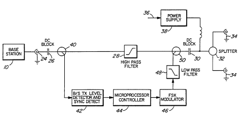
Referring now to Figure 2, which illustrates the base station extender 12 in
greater detail, a connector
24, which is connected to the base station 10, is connected through a DC
blocking capacitor 26, a
2~3436~
_g_
high pass filter 28 and a second DC blocking capacitor 30 to a splitter 32,
which is provided with
two co-axial connectors 34 for connection to the co-axial cables 14 and 16.
In the case, for example, that the telephone system is implemented to operate
in accordance with the
CT-2 Plus standard (TDD-FDMA), the base station 10 will output the transmit
signal for one
millisecond at 944 MHz and will then receive the receive signal for one
millisecond at 944 MHz.
The transmission from the base station 10 is typically at a high signal level,
e.g. 10 milliWatts, while
the receive signals are typically at a low power level, e.g. 1 nanoWatt.
The basestation extender 12 also has a power input conductor 36, which is
connected from an
alternating current supply (not shown) to a power supply 38, which outputs DC
or low frequency
AC power through the splitter 32 to the central conductors of the co-axial
cables 34 for powering
the remote microcell extenders 18 and 19.
Between the DC blocking capacitor 26 and the high pass filter 28, there is
connected a directional
coupler 40, which connects a portion of the base station transmit signal to a
first signal power level
detector 42, which comprises a standard diode detector circuit. Whenever the
base station transmits
a signal for 1 millisecond, the signal level at the detector 42 produces a 1
millisecond pulse having
a pulse height proportional to the magnitude of the transmit signal from the
base station 10. This
pulse is supplied to a microprocessor controller 44, which quantises the
height of the pulse and
encodes signal level data, representing the pulse height, in a data stream
which is modulated, by a
frequency shift keyed (FSK) modulator 46, onto a 10.7 MHz subcarrier as data,
as described in
greater detail below. The modulated signal level data then passes through a
low pass filter 48 to a
directional coupler 50, connected between the high pass filter 28 and the DC
blocking capacitor 30,
for transmission through the co-axial cables 14 and 16 to the microcell
extenders 18 and 19. In the
present embodiment of the invention, the microprocessor controller 44 is
implemented as a Motorola
68HC 11 microprocessor with on-chip analog-to-digital converters.
~1343G5
-9-
It is pointed out that the directionality of the directional coupler, 40
favours pickup of transmit
signals from the base station 10, and does not favour pickup of receive
signals from the handset 22.
This directionality, in association with the difference in magnitude of the
transmit and receive
signals, allows the microprocessor controller 44 to differentiate simply
between the transmit signals
and the receive signals. As a consequence of being able to recognize the
transmit signal pulses from
the receive pulses, the microprocessor controller 44 can use the level
detector 42 to define the
transmit/receive timing necessary for synchronization of the second RF
repeater parts. This method
of deriving transmit receive timing is only useful once a handset has an
established signal link with
a base station (i.e. there is a valid transmit pulse from the base station to
detect). This method is
generally not applicable in the absence of a base station-handset link.
In the absence of such a link, it is possible to use a CSC or beacon signal
from the base station to
provide timing. Thus, for example, in the case of the CT-2 Plus protocol, a
signal in the form of a
regular RF burst from the base station (the CSC) is guaranteed in the absence
of a base station-
handset link. Thus, for CT-2 Plus, the CSC may be used to provide full
transmit-receive timing at
all time epochs, when used in conjunction with timing derived during a voice
link.
This transmit/receive timing is encoded into the FSK data stream by the
microprocessor controller
44.
The microcell extender 18 is shown in greater detail in the block diagram of
Figure 3 is intended for
TDD operation using the CT-2 Plus protocol, and it is to be understood that
the microcell extenders
18 and 19 are similar to one another.
As shown in Figure 3, the microcell extender 18 has an input in the form of a
co-axial connector 52
for connection to the co-axial cable 14. The co-axial connector 52 is
connected through a DC
blocking capacitor 54, a directional coupler 56, a high pass filter 58 and a
variable attenuator 60 to
the input of a band limited TDD amplifier 62. As described below, the variable
attenuator 60 and
the amplifier 62 form a signal level regulator for adjusting the levels of the
transmit and receive
2134365
- to -
signals. The output of the band limited TDD amplifier 62 is connected through
a directional coupler
64 and the output of the microcell extender 18 to the antenna 20.
The co-axial connector 52 is also connected to a DC switching regulator 64,
the output of which
provides DC power to all the electronic circuits in Figure 3.
The directional coupler 56 supplies a portion of the incoming signal, from the
co-axial cable 14,
through a lowpass filter 66, to preferentially pass the 10.7 MHz signal, to a
10.7 MHz frequency shift
keyed demodulator 68, the output of which contains the signal level data and
the transmit-receive
synchronization data provided, as described above, by the base station
extender 12.
A portion of the output of the band limited TDD amplifier 62 is supplied by
the directional coupler
64 to a second level detector 70, which detects the power level of the
amplified transmit signal being
supplied to the antenna 20 and provides this level to a control device in the
form of a microprocessor
controller 72.
The level detector 70 is implemented by a circuit identical to that of the
level detector 42 in Figure
2, i.e. a standard diode detector circuit. This will often result in some
easing of temperature,
tolerancing and linearity constraints since the use of identical level
detectors 70 and 42 will typically
result in these imperfections cancelling out.
The signal level data output from the demodulator 68 is compared in the
microprocessor controller
72 with the quantised level from the level detector 70 to determine the
difference in the levels of the
transmit signal at the base station extender 12 and at the microcell extender
18 and the
microprocessor controller 82 correspondingly adjusts the variable attenuator
60 so as to cause the
level of the amplified transmit signal supplied to the antenna 20 to a
predetermined ratio, e.g. 1:1,
relative to that of the transmit signal detected by the level detector 42 of
Figure 2.
213~36~
-11-
Consequently, the microcell extender 18 will adjust its output so that the
signal level at the antenna
20 is e.g. substantially identical to that at the output of the base station
10. The same holds true for
the transmit signal level at the antenna 20 of the microcell extender 19.
The directional coupler 64 has a preference for coupling the transmit signal
power to the power
detector 70, and does not couple the receive signal power well.
Reference is now made to Figures 4a and 4b, which show in greater detail the
band limited time
division duplex amplifier 62, which comprises a pair of amplifiers 72 and 74
connected in series,
with a band limiting filter 76 connected between the amplifiers 72 and 74. The
output of the
amplifier 76 and the input of the amplifier 72 are connected to respective
terminals of a transfer
switch indicated generally by reference numeral 78. The antenna 20 and a
conductor 80, extending
from the variable attenuator 60, are connected to two other terminals of the
transfer switch 78.
The transfer switch 78 has two switch states. As shown in Figure 4A, in a
first switch state, which
is a "receive" state in which the receive signal from the handset 22 is being
received by the antenna
20, the transfer switch 78 connects the antenna 20 to the input of the
amplifier 72 and also connects
the output of the amplifier 78 to the variable attenuator 60, so that the
receive signal is amplified by
the amplifiers 72 and 74 and the gain is controlled by the variable attenuator
60 so as to counteract
attenuation between the antenna 20 and the base station 10.
In a second switch state of the transfer switch 78, as illustrated in Figure
4B, the conductor 80 from
the variable attenuator 60 is connected to the input of the amplifier 72,
while the output of the
amplifier 74 is connected to the antenna 20. In this "transmit" state,
therefore, the transmit signal,
after attenuation by the variable attenuator 60, is amplified by the
amplifiers 72 and 74 to counteract
signal loss between the base station and the antenna 20, as described above.
_21343~~
-12-
The changes in the state of the transfer switch 78 are controlled by control
outputs from the
microprocessor controller 72 in accordance with the timing derived from the
transmit and receive
signals.
Thus, the amplifiers 72 and 74 are used to amplify both the transmit signals
and also the receive
signals, and the transmit and receive signal gains are equal. The amplifier
and switch arrangement
shown in Figures 4A and 4B therefore enables the microcell extender 18 to
automatically
compensate for both the transmit signal loss from the base station 10 to the
antenna 20 and, also, the
receive signal loss from the antenna 20 to the base station 10.
Figure 5 shows a modification of the telephone system illustrated in Figure 1.
More particularly,
in the modification illustrated in Figure 5, an in-line amplifier unit 90,
which is similar to the
microcell extenders 18 and 19, is connected between the base station extender
12 and the microcell
extender 19 for amplifying the transmit and receive signals passing through
the co-axial cable 16,
and to relay the boosted signals to the microcell extender 19 or the base
station extender 12, as the
case may be.
The in-line amplifier unit 90 is similar to the microcell extender 18 shown in
Figure 3, except that,
the antenna 20 is omitted and is replaced by a co-axial connector 91 for
connection to a co-axial
cable 16A extending to the microcell extender 19. This arrangement allows
microcell extender 10
to be connected to the base station by a physically longer, and hence more
lossy, length of co-axial
cable.
As shown in Figure 3, a bypass conductor 92 interconnects the co-axial
connectors 52 and 91, i.e.
the input and output of the in-line amplifier unit 90 and is provided with a
switch 94. Closure of the
switch 94 connects the 10.7 MHz subcarrier and the power from the connector 52
to the connector
91 and, thus, to the microcell 19.
_2134365
-13-
When employing this in-line configuration, it is generally preferable to set
the output level of the in-
amplifier unit 90 lower than the usual transmit level. This allows the
cascaded intermodulation
budget for the in-line amplifier unit 90 and the end-of line microcell
extender 19 to be dominated
solely by the end-of line performance. Therefore, in operation, the closure of
the switch 94 is
detected by the microprocessor controller 72 and the variable attenuator 60 is
adjusted by the
microprocessor controller 72 in order to ensure that the detected signal level
at connector 91 is,
typically, one tenth of the signal output level at the base station 10. The in-
line transmit gain will
equal the in-line receive gain.
As described above, the transmit and receive signals are in the form of time
division duplex signals.
However, the above-described apparatus of Figures l, 2 and 3 can be readily
adapted for frequency
division duplex operation.
For this purpose, the band limited TDD amplifier 62 of Figure 3 is replaced by
a band limited FDD
amplifier 100, as shown in Figure 6. The remaining components of the microcell
extender shown
in Figure 6 are similar to those of Figure 3 and, therefore, have been
referenced by the same
reference numerals and will not again be described herein.
The band limited FDD amplifier 100 of Figure 6 is illustrated in greater
detail in Figure 7.
As shown in Figure 7, a conductor 102, from the variable attenuator 60, is
connected to a duplexer
104, which supplies the transmit signal through a band limiting filter 106 to
a transmit amplifier 108,
and which receives, from a band limiting filter 110 and a receive signal
amplifier 112, the receive
signal, which is then supplied through the conductor 102 to the variable
attenuator 60.
The output of the transmit signal amplifier 108, and the filter 110 are
connected to a further duplexer
114, which is connected through the directional coupler 68 to the antenna 20.
The duplexers 104 and 114 may, if required, be replaced by RF
splitters/combiners.
21343fi5
-14-
In the FDD arrangement, the transmit amplifier 108 and filter 106 are
physically distinct from the
receive amplifier 112 and filter 110. Since the transmit signal levels are
typically many orders of
magnitude larger then the receive signal levels, the power detectors 42
(Figure 2) and 70 (Figure 3)
can easily be used by the microprocessor 72 to distinguish the transmit power
levels from the receive
signal power levels. Provided that the receive amplifier 112 of Figure 7 has a
known gain relative
to the transmit amplifier 108, the receive path gain between the antenna 20
and the base station 10
is again well controlled and determined by the signal level adjustment
employed for the transmit
signal gain.
The operation of the microprocessor 44 in Figure 2 employs the following
steps:
1. Measure the level from the detector 42.
2. If the level corresponds to a signal of more than (say), one-tenth of a
milliWatt, assume the
level represents a transmit pulse.
If the level is smaller than one-tenth of a milliWatt, assume the level
represents a receive
pulse.
3. If a transmit pulse is present, send the level data to the FSK modulator 46
for transmission
to all second part RF repeaters.
If a receive pulse is present, send message "Rx Present" to all second RF
repeater parts.
4. If a transmit pulse is present, but the previous measurement indicated a
receive pulse,
designate this measurement as the "start of the transmit pulse."
S. Send this "start of transmit pulse" data to the FSK modulator 46 for
transmission to all
second part RF repeaters.
213436
-15-
6. Repeat the level measurement (i.e. return to step 1).
Given this sequence, the microprocessor 72 of Figure 3 will typically operate
as follows, for the
concrete example of CT-2 Plus, which has 1 ms transmit and 1 ms receive
epochs.
1. Read the data from the FSK demodulator 68.
2. If the data reads "start transmit pulse", start a software counter that
will place the transfer
switch 78 into the receive position, in 1 milliseconds time, and into the
transmit position in
2 millisecond time.
3. If the data gives a transmit signal level, read the level of that instant
from level detector 70.
4. If the switch 94 is closed (in-line mode), multiply the signal level
recorded by the level
detector 70 by ten.
If the switch 94 is open (end-of line mode) multiply the signal level recorded
by the level
detector 70 by one.
5. If the level from the level detector 70 is larger than the level read at
the demodulator 68,
increase the attenuation at the variable attenuator 60 by a small increment.
If the level from 70 is smaller than the level read at the demodulator 68,
reduce the
attenuation at the variable attenuator 60 by a small increment.
6. Repeat step 1 onwards.
2134365
- 16-
Note that these software steps may result in the RF repeater being
dysfunctional for two or three
hundred milliseconds, when first powered up, but fully functional thereafter.
In practice this is not
a problem.
Of course, more sophisticated programs may be used, e.g.
- the microprocessor in Figure 3 may average the results of many measurements
before
deciding when the "start of transmit" really occurs, or what the transmit
level really is.
- as has been noted, CT-2 Plus provides a burst of CSC's in the absence of a
voice link. The
CSCs consist of three bursts of 1 millisecond each, every 72 milliseconds.
Under these circumstances, the microprocessor 72 of Figure 2, performs the
additional step
of creating its own "start of transmit" pulse for step 2 if previous "start of
transmit"pulses
indicate it is now a transmit epoch, but the level data reads "Rx present", in
contradiction to
prior experience.
The operation of the microprocessors 72 and 44, has so far been described for
TDD operation.
In fact similar software can be employed for FDD operation vis-a-vis level
control, but the timing
control software may be limited to assisting in FDD-TDMA systems to selecting
certain time slots
for broadcast/reception by certain array members.
Various modifications may be made in the above-described apparatus within the
scope and spirit of
the appended claims. For example, it may in some cases be useful to employ
heterodyne techniques
in the RF repeater arrangements of Figures 4 or 7. Also, instead of employing
a variable attenuator
and an amplifier to adjust the signal levels as described above, it may be
appropriate in some
circumstances to employ a variable gain amplifier for that purpose.