Note: Descriptions are shown in the official language in which they were submitted.
~135856
LOW POWER, ADDRESSABLE DATA COMMUNICATION DEVICE
AND METHOD
TECHNICAL FIELD OF THE INVENTION
The present invention relates generally to
addressable data communication devices wherein many
devices may receive the same data communication messages,
and the messages have addresses or identification codes
that define which device or devices should respond to the
messages. In addition, the present invention relates to
data communication devices in which energization to
various components is managed to reduce power consumption.
BACKGROUND OF THE INVENTION
Data communication devices receive data from other
data communication devices and/or transmit data to other
data communication devices. Data communication devices
are often addressable when more than two devices share a
common communication channel. An address is a data code
that uniquely identifies a device or a set of devices.
When a data message transmitted through the common
communication channel conveys an address, such as a phone
number, path, ID code, or the like, a device that receives
the data message decodes the address to determine what to
do with the message.
Electronic tags represent one form of data
communication device known to those skilled in the art.
Electronic tags are low cost transponders which receive
and transmit data messages via radio frequency (RF)
signals. Typically, an interrogator transmits a data
message which contains an ID code. All tags within range
of the interrogator receive this data message. The ID
code addresses a particular tag or category of tags. Each
tag that receives the data message determines whether its
ID or a category to which it belongs matches the address
conveyed by the data message. If a tag determines that
the data message is addressed to it, the tag processes the
data message and typically responds by transmitting its
own data message back to the interrogator.
--1--
~13585~
-
Electronic tags are often battery powered. In order
to increase battery life, conventional tags are maintained
in a very low current, standby state until they sense RF
energy from an interrogator. When a conventional tag
detects such RF energy, it goes into a high current,
operational state by powering up all its circuitry. Once
operational, the conventional tag processes the received
data message. In one of the first tasks performed after
becoming operational, the conventional tag determines
whether the received data message is actually addressed to
the tag. If the data message is addressed to the tag, the
tag continues to process the message and respond with
requested information. After the tag completes the
transaction, it again returns to its low current, standby
state. If the data message is not addressed to the
conventional tag, it directly returns to its low current,
standby state.
This power management scheme works acceptably well in
scenarios where tags are associated with moving objects,
such as vehicles, railroad cars, trucks, or other objects
which are interrogated only occasionally. However, where
tags are associated with stationary objects, such as in a
warehouse or inventory management environment, or with
other objects which tend to receive numerous
interrogations, battery life is severely shortened. In
inventory management and other situations, many tags can
be within range of an interrogator at all times. Each
time an interrogator addresses an interrogation to a
particular tag, all tags within range go to their high
current, operational states. However, only the addressed
tag actually processes the interrogation to any
significant extent and responds to the interrogation.
SUMMARY OF THE INVENTION
Accordingly, it is an advantage of the present
invention that an improved low power, addressable data
communication device is provided.
213~56
-
Another advantage of the present invention is that an
electronic tag with improved battery life is provided.
Another advantage is that the present invention
allows an electronic tag to remain in a low current,
standby state while in the presence of an interrogation
signal except for when the tag is specifically addressed
by the interrogation signal.
Another advantage is that the present invention
provides separate decoding paths for obtaining data from
an interrogation signal, wherein a separate decoding path
permits a low power decoder to control energization of a
high power decoding path.
Another advantage is that the present invention
includes a power manager that decodes a portion of an
interrogation signal while consuming very little power.
The above and other advantages of the present
invention are carried out in one form by a low power,
addressable data communication device and associated
method. The device includes some means for obtaining a
data message having a wake-up section and a session
section. The device also includes a power manager. The
power manager has an input coupled to the obtaining means
and has an output. The power manager is configured to
detect a predetermined identification code from the wake-
up section of the data message. The device furtherincludes a controller. The controller has a power input
coupled to the power manager output and has a data input
coupled to the obtaining means. The controller is
configured to process the session section of the data
message after the power manager detects the predetermined
identification code.
BRIEF DESCRIPTION OF THE DRAWINGS
A more complete understanding of the present
invention may be derived by referring to the detailed
description and claims when considered in connection with
the Figures, wherein like reference numbers refer to
similar items throughout the Figures, and:
- 2135856
FIG. 1 shows a block diagram of an electronic tag
configured in accordance with the principles of the
present invention;
FIG. 2 shows a data format diagram of an
interrogation data message;
FIG. 3 shows a data format diagram of a wake-up
section of the interrogation;
FIG. 4 shows a block diagram of a decoder portion of
a power manager block from the electronic tag shown in
FIG. l;
FIG. 5 shows a timing diagram which depicts exemplary
signals associated with the decoder illustrated in FIG. 4;
FIG. 6 shows a block diagram of a synchronizer
portion of the power manager;
FIG. 7 shows a block diagram of an ID detector
portion of the power manager; and
FIG. 8 shows a block diagram of an end detector
portion of the power manager.
DETAILED DESCRIPTION OF THE PREFERRED EMBODIMENTS
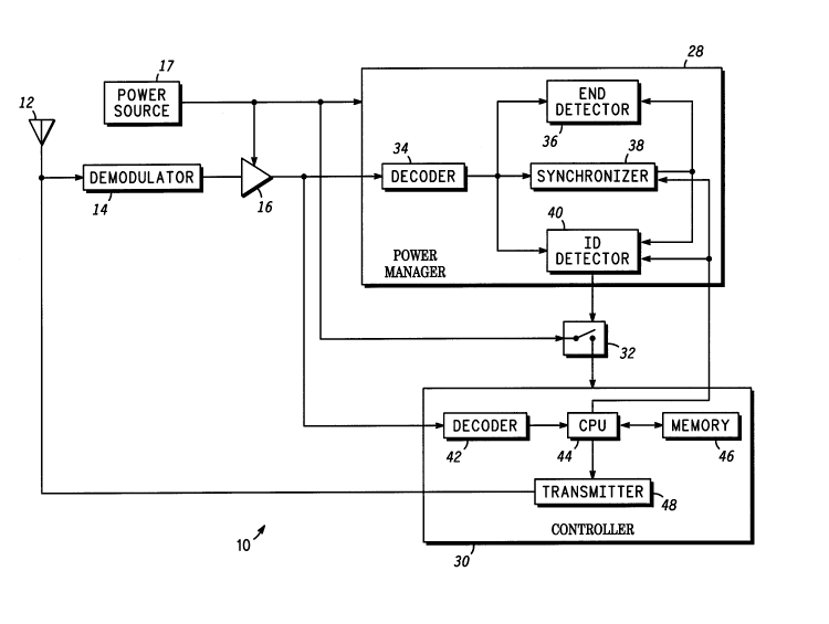
FIG. 1 shows a block diagram of electronic tag 10
configured in accordance with the principles of the
present invention. Tag 10 is a data communication device
which receives and transmits data messages, preferably
through radio frequency (RF) signals. Tag 10 may be used
in applications where it is desirable to identify and
track specific objects. A population of tags 10 may be
associated with a corresponding population of objects,
e.g., vehicles, railroad cars, trucks, inventory items,
employees, etc. Each tag 10 desirably has its own unique
identification code. Interrogators (not shown) may be
placed near areas where the objects may be located or near
transportation routes over which the objects may pass.
Each interrogator may, from time to time, transmit RF
signals to tags 10 within range of the interrogator. The
interrogation signals may request a specific tag 10, any
tag 10 from a specified class of tags 10, or any tag 10
from the population of tags 10 to respond by transmitting
` 2135856
an RF response signal back to the interrogator. The
interrogation may request tag 10 to store data and/or to
transmit various items of data in response.
Tag 10 includes antenna 12 into which RF
interrogation signals are received and from which RF
response signals are transmitted. Antenna 12 couples to
demodulator 14, which strips RF modulation away from a
data message conveyed by a received interrogation signal.
In the preferred embodiment, demodulator 14 is implemented
using passive components and consumes no battery power.
Demodulator 14 couples to an input of low power amplifier
16. Amplifier 16 desirably includes active components
which couple to power source 17, e.g., a battery.
Amplifier 16 desirably remains energized in both standby
and operational states. However, amplifier 16 uses
conventional low power amplification circuits which
preferably consume only a few micro amps.
Thus, amplifier 16 obtains a data message from which
a carrier signal has been stripped. However, data
conveyed by the data message may still be, and desirably
are, encoded or modulated in some way. When data, such as
the data message obtained by amplifier 16, are
communicated serially, a data-communicating signal
expresses one data element at one point in time, another
data element at another point in time, and so on. Since
the data change in time, some transition period exists
between the instants where data elements are expressed
through the communicating signal. In communicating data,
communication systems encode and/or modulate the data-
communicating signal. The encoding and/or modulation areperformed, among other reasons, to help a receiving data
communication device to distinguish instants in time where
the data-communicating signal is expressing data elements
from data transition periods, and to accurately identify
the conveyed data elements.
FIG. 2 shows a data format diagram of preferred
interrogation data message 18 which is obtained from an
interrogator. Data message 18 (FIG . 3) includes wake-up
21358~6
section 20 followed by session section 22. Desirably,
wake-up section 20 is encoded in a manner which combines a
clock signal with data, e.g., Manchester coding. The
clock signal conveys timing information indicating when
data are valid (not transitioning). Such encoding schemes
may be decoded by relatively simple circuits which consume
less power than more complex circuits. Wake-up section 20
desirably conveys data at a relatively slow data rate,
preferably less than 17 kHz, further contributing to low
power consumption by decoding circuits. On the other
hand, session section 22 may experience a different
encoding scheme which desirably operates at a faster data
rate than wake-up section 20.
FIG. 3 is a data format diagram of preferred wake-up
section 20 of data message 18 (FIG. 2). Wake-up section
20 includes preamble 24 followed by identification code
26. Preamble 24 represents a predetermined code which
helps tags 10 (FIG. 1) find the beginning of
identification code 26. Desirably, preamble 24 conveys
the same code from interrogation to interrogation and from
tag 10 to tag 10. While the preferred embodiment of the
present invention uses the four bit code of "1100" for
preamble 24, any length and any code for preamble 24
suitable for indicating synchronization may be used.
Identification code 26 represents a wake-up address
that may or may not be unique to a given tag 10. When tag
10 determines that wake-up section 20 conveys
identification code 26 assigned to that tag 10, that tag
10 becomes fully operational so that it may process and
respond to session section 22 (FIG. 2). While the
preferred embodiment of the present invention uses
identification code 26 of length N = 16, length N may vary
to meet varying needs of specific applications.
Session section 22 (FIG. 2) may include any type of
data that an interrogator may wish to communicate to tag
10. Such data may serve as instructions to tag 10 which
cause tag 10 to take a specified action, e.g., reading or
writing data. Such data may include addressing or
2135856
identification data and password data which tag 10
e~mines prior to following any instructions. Thus, if
identification code 26 (FIG. 3) does not present a unique
code within a population of tags 10, a specific individual
tag 10 may be uniquely identified by the combination of
identification code 26 and any addressing or
identification data included in session section 22.
The output of amplifier 16 ( FIG. 1) couples to data
inputs of power manager 28 and controller 30. Power
source 17 couples to a power input of power manager 28.
Power manager 28 remains continuously energized, at least
during the standby state. An output of power manager 28
couples to a control input of switching circuit 32. Power
source 17 and a power input of controller 30 couple to
signal ports of switching circuit 32. Thus, controller 30
is energized through switching circuit 32 under the
control of power manager 28.
Power manager 28 includes decoder 34 configured to
separate a clock signal from wake-up data during wake-up
section 20 of data message 18 ( FIG. 2). Clock and data
outputs from decoder 34 couple to inputs of end detector
36, synchronizer 38, and ID detector 40. End detector 36
identifies when the end of identification code 26 and
wake-up section 20 occur (FIG. 3). Synchronizer 38
detects occurrence of preamble 24, and ID detector 40
determines when a predetermined identification code
follows the preamble. The identification code may vary
from tag 10 to tag 10.
ID detector 40 provides the output from power manager
28 which couples to the control input of switching circuit
32. When ID detector 40 discovers the identification code
for tag 10, switching circuit 32 is directed to energize
controller 30. When ID detector 40 fails to discover the
identification code for tag 10, switching circuit 32 is
directed to refrain from energizing controller 30.
Controller 30 includes decoder 42, which has a data
input that couples to the output of amplifier 16. Tag 10
includes two separate decoders for data conveyed through
-- 2135856
data message 18 (FIG. 2), one residing in power manager 28
and another in controller 30. Use of two separate
decoders permits diverse encoding schemes in wake-up
section 20 and session section 22, allowing decoder 34 and
wake-up section 20 to be optimized for low power operation
while decoder 42 and session section 22 are optimized for
other purposes. Decoder 42 is preferably a general
purpose decoder which may reliably decode data encoded or
modulated in a variety of different schemes and at a
variety of different data rates, including data rates far
faster than that associated with wake-up section 20.
Decoder 42 may be optimized for flexibility, desirable
signal to noise ratios, and/or efficient spectrum
utilization, rather than for low power operation.
An output of decoder 42 couples to central processing
unit (CPU) 44, which may be embodied in a conventional
microprocessor circuit. CPU 44 couples to memory 46 and
transmitter 48. Transmitter 48 additionally couples to
antenna 12. CPU 44 also couples to synchronizer 38 and ID
detector 40 of power manager 28. CPU 44 obtains and
processes data conveyed by data message 18 during session
section 22 ( FIG. 2). CPU 44 generates data which are
routed through transmitter 48 and transmitted from antenna
12. Memory 46 stores a unique identifying code that is
associated with tag 10 and programming instructions which
define tasks performed by CPU 44 and controller 30.
Memory 46 preferably may also save data received at tag 10
during an interrogation and other variables. CPU 44
couples to synchronizer 38 and ID detector 40 so that it
may store data into various registers to control the
operation of power manager 28. Under normal operating
conditions, CPU 44 and controller 30 perform these
functions only when wake-up section 20 of data message 18
conveys a recognized identification code 26 (FIG. 3).
While FIG. 1 shows decoder 42 as a separate component
from CPU 44, in an alternate embodiment (not shown)
decoder 42 and CPU 44 may both be substantially
implemented in a common microprocessor circuit.
--8--
21358S6
FIG. 4 is a block diagram of decoder 34 of power
manager 28 (FIG. 1), FIG. 6 is a block diagram of
synchronizer 38, FIG. 7 is a block diagram of ID detector
40, and FIG. 8 is a block diagram of end detector 36. The
configurations of decoder 34, synchronizer 38, ID detector
40, and end detector 36 allow power manager 28 to monitor
wake-up sections 20 of messages 18 ( FIG. 2) while
consuming very little power. Power manager 28 consumes
less power than any other component within controller 30.
Decoder 34 (FIG. 4) includes free-running, low
current, real time clock oscillator circuit 50,
preferably consuming less than one micro Ampere and
generating a clock signal oscillating at around 32.768
kHz. While other embodiments of the present invention may
certainly accommodate oscillators operating at other
frequencies, this specific frequency is beneficial because
it is relatively slow insofar as electronic circuits are
concerned. Oscillator 50 controls the rate at which power
manager 28 experiences voltage changes taking place when
the various digital signals within power manager 28 ( FIG.
1) change states. Various semiconductor technologies,
e.g., CMOS (preferred in the present invention due to its
low power consumption), consume less power in a given
period of time when fewer voltage changes take place in
the given period of time. Thus, use of a slow oscillator
50 greatly contributes to the low power consumption of
power manager 28. In addition, the preferred frequency
for oscillator 50 is useful in the watch industry.
Consequently, inexpensive, very low power, and reliable
designs for oscillator 50 are well known.
Oscillator 50 couples to an edge discriminator
circuit including delay element 52 and Exclusive OR gate
54. The duration parameter of delay element 52 produces a
clock pulse for counter 56. An output of gate 54 produces
a pulse every time the oscillation signal from oscillator
50 changes state, i.e., a clock signal having double the
frequency of the oscillation signal from oscillator 50.
21358~B
The output from gate 54 couples to a clock input (C)
of counter 56, which is configured to count from a reset
state for a number of counts chosen in accordance with the
data rate of wake-up section 20 (FIG. 2) of data message
18. The number of counts is chosen so that an output from
counter 56 oscillates at approximately twice the data
rate. Counter 56 preferably divides by two when this data
rate is around 16 kHz or divides by four when this data
rate is around 8 kHz.
The received encoded data signal from amplifier 16
(FIG. 1) is supplied to an edge discriminator that
includes delay element 58 and Exclusive OR gate 60. Gate
60 generates a pulse every time the received encoded data
signal changes states. The output of gate 60 couples to a
reset (R) input of counter 56. Counter 56 is reset every
time the received encoded data signal changes states.
FIG. 5 is a timing diagram depicting exemplary
signals associated with the embodiment of decoder 34
illustrated in FIG. 4. With reference to FIGs. 4 and 5,
waveform A depicts an exemplary Manchester coded, received
data signal which conveys data bits, "1011" in this
example (any data combination may be supplied). A data
clock is combined with the data. The data are conveyed by
transitions which occur in the middle of each bit 62
(timing depicted by vertical dotted lines, FIG. 5). The
output from counter 56 (waveform B), represents a free-
running signal that oscillates at roughly double the bit
rate for signal A. The output of gate 60 re-synchronizes
waveform B to the edge transitions of waveform A.
The output from counter 56 couples to clock inputs
(C) of flip flops 64 and 66. Flip flop 64 is configured
to toggle, with an inverting output (NQ) coupled to a data
input (D). A non-inverting output (Q) of flip flop 64
provides a data clock (waveform C, FIG. 5). This output
provides the data clock signal output of decoder 34. Flip
flop 64 essentially divides the double frequency clock
(waveform B) by two and squares up any lack of symmetry.
The starting state of flip flop 64 is unknown relative to
-10-
2135856
the reset state of counter 56. Waveform C may be inverted
from the polarity shown in FIG. 5.
The received encoded data signal (waveform A), is
applied to a data input (D) of flip flop 66. Non-
inverting outputs of flip flops 66, 64 couple to inputs of
Exclusive OR gate 68. The non-inverting output of flip
flop 66 provides a Manchester coded data signal
synchronized to the data clock produced by flip flop 64
(e.g., waveform D). Gate 68 separates the data clock from
this synchronized Manchester coded data signal (e.g.,
waveform E). Waveform F illustrates bit timing associated
with waveform E.
While gate 68 generates decoded data from the
Manchester coded data signal, these data are provided in
an ambiguous form. Due to the uncertainty associated with
the state of flip flop 64 relative to the resetting of
counter 56, these data are provided in either an inverted
or non-inverted form. Data generated by gate 68 and by
decoder 34 exhibits an unknown or ambiguous polarity.
Accordingly, a preferred embodiment of decoder 34
generates clock and data signals using only two flip
flops, a small counter, three gates, two delay elements,
and a low frequency oscillator circuit. These few
components consume a very small amount of current. While
decoder 34 could be configured to resolve the polarity
ambiguity associated with the data output, this requires
additional components and leads to additional power
consumption while achieving little added benefit.
FIG. 6 is a block diagram of synchronizer 38. The
ambiguous decoded data from decoder 34 (FIGs. 1, 4) are
applied to a data input (D) of serial shift register 70
and to a first input of Exclusive OR gate 72. The data
clock from encoder 34 is applied in the preferred
embodiment to only a first input of an enabling circuit
74, illustrated in FIG. 6 as a NOR gate. An end signal
which is generated by end detector 36 (FIG. l) is applied
to a reset input (R) of shift register 70. The end signal
213585B
clears shift register 70 shortly after the end of wake-up
section 20 ( FIG. 2).
A data bus from controller 30 couples to inputs of
inverted synchronization (sync) pattern register 76 and to
sync pattern register 78. At some point when controller
30 is energized, controller 30 writes preamble 24 (FIG.
3), i.e. r'll00" in the preferred embodiment, to register
78, and controller 30 writes the preamble inverted, i.e.
"0011" in the preferred embodiment, to register 76.
Registers 76, 78 retain these preamble data while
controller 30 is de-energized.
An output from enabling circuit 74 couples to a clock
input (C) of shift register 70. A parallel output from
shift register 70 couples to respective first inputs of
comparison circuits 80, 82. An output of inverted sync
pattern register 76 couples to a second input of
comparison circuit 80, and an output of sync pattern
register 78 couples to a second input of comparison
circuit 82. An output of comparison circuit 80 couples to
a second input of Exclusive OR gate 72, and outputs of
comparison circuits 80, 82 couple to respective inputs of
OR gate 84. Exclusive OR gate 72 provides a decoded data
signal representing the ambiguous data signal from decoder
34 ( FIG. 4) with the ambiguity resolved. OR gate 84
provides a sync signal that activates when preamble 24
(FIG. 3) is detected. The output of OR gate 84 is fed
back to a second input of enabling circuit 74.
So long as synchronizer 38 has not yet found preamble
24 ( FIG. 3), the data clock clocks ambiguous decoded data
into shift register 70. Comparison circuits 80, 82
continuously determine whether the pattern recorded in
register 70 matches the inverted or the non-inverted
preamble. As soon as either of the inverted or non-
inverted preambles is discovered, gate 84 activates the
sync signal, freezing the clock to register 70, which then
retains the detected preamble pattern, and synchronizer 38
becomes disabled with its sync output signal active. The
21358S6
sync signal r~; n.~ active until the end signal clears
register 70 at the end of wake-up section 20.
Disabling synchronizer 38 causes the voltage changes
experienced by synchronizer 38 to largely cease, causing
drastically decreased power consumption. Enabling circuit
74 is configured to reduce the power consumption of
synchronizer 38 after the sync signal activates.
Synchronizer 38 consumes only a minuscule amount of power
during identification code 26 of wake-up section 20 (FIG.
3). As discussed above, decoder 34 is desirably
configured so that the data clock signal does not
experience voltage changes during session section 22 ( FIG.
2) and when no interrogation is being received. Thus,
synchronizer 38 consumes a notable amount of power only
during preamble 24 of wake-up section 20, and this notable
amount is much less than the power consumed by any other
component within controller 30 (FIG. 1).
Synchronizer 38 detects either the inverted or non-
inverted preamble because the ambiguous decoded data from
decoder 34 (FIG. 4) may present the preamble in either an
inverted or non-inverted state. In addition, this adds
robustness to the design of tag 10. Other devices in the
communication channel through which interrogations are
transmitted may or may not insert amplification stages
etc. which invert their signals. Due to the ability of
synchronizer 38 to handle ambiguous decoded data, tag 10
operates successfully regardless of the received signal
polarity. Exclusive OR gate 72 removes ambiguity by
inverting ambiguous decoded data when an inverted preamble
is detected and not inverting the ambiguous decoded data
when a non-inverted preamble is detected.
FIG. 7 is a block diagram of ID decoder 40.
Unambiguous decoded data from synchronizer 38 ( FIGs. 1, 6)
are applied to a data input (D) of serial shift register
86. The data clock from decoder 34 is preferably applied
to only a first input of enabling circuit 88, illustrated
in FIG. 7 as a NAND gate. The sync signal from
synchronizer 38 is applied to a second input of enabling
2135856
circuit 88, and an output of enabling circuit 88 couples
to a clock input (C) of shift register 86. The data bus
from controller 30 (FIG. 1) couples to an input of an ID
code register 90. A multi-bit, parallel output from
register 90 couples to a first input of a comparison
circuit 92, and a parallel output from shift register 86
couples to a second input of comparison circuit 92. An
output of comparison circuit 92 couples to a data input of
flip flop 94 whose clock input is adapted to receive the
end signal generated by end detector 36. The end signal
clocks flip flop 94 shortly after the end of
identification code 26 (FIG. 3). The output from flip
flop 94 provides a wake-up signal that serves as the
output from both ID detector 40 and power manager 28.
A reset signal from controller 30 (FIG. 1) couples to
a reset input of register 86 and to a reset input of flip
flop 94. When controller 30 finishes its interrogation
session and tag 10 no longer needs to be in its
operational state, controller 30 may activate this reset
signal to clear register 86 and flip flop 94, thereby de-
energize controller 30 and returning tag 10 to a standby
state.
At some point when controller 30 is energized,
controller 30 writes identification code 26 (FIG. 3) to
register 90. The identification code may be unique to tag
10 or it may classify tag 10 into a class with other tags
10 that have the same identification code. Nothing
prevents the identification code from changing over time,
and such changes can be accommodated by performing
interrogations on tag 10 that instruct controller 30 to
write specified data to register 90. Register 90 retains
its identification code while controller 30 is de-
energized.
Until the sync signal from synchronizer 38 (FIG. 6)
activates, enabling circuit 88 holds ID decoder 40 in a
disabled, frozen state, causing ID decoder 40 to consume
only a minuscule amount of power. Enabling circuit 88 is
configured to reduce the power consumption of ID decoder
-14-
2135856
40 before activation of the sync signal compared to its
power consumption after activation of the sync signal.
After the sync signal activates, the data clock from
decoder 34 clocks the decoded data from synchronizer 38
into shift register 86. If, at the end of identification
code 26 (FIG. 3), data held in register 86 matches the
identification code recorded in register 90, the wake-up
signal is activated, and tag 10 enters its operational
state. If the data held in register 86 do not match, the
wake-up signal rr~i n.~ inactive and tag 10 remains in its
standby state.
In an alternate embodiment, ID detector 40 may
include duplicate ID registers 90 and comparison circuits
92 whose outputs are combined in an ORing circuit (not
shown) and routed to flip flop 94. In this embodiment, a
specific identification code may be stored in one register
while a class or category code is stored in the other
register. If identification code 26 (FIG. 3) of wake-up
section 20 conveys either the specific identification code
or the class code, tag 10 enters operational state so that
it can process and respond to data conveyed during session
section 22 (FIG. 2).
FIG. 8 is a block diagram of end detector 36. The
data clock from decoder 34 (FIG. 4) is preferably applied
to only a first input of enabling circuit 98, illustrated
as a NAND gate. The sync signal from synchronizer 38
(FIG. 6) is applied to a second input of enabling circuit
98, and an output of enabling circuit 98 couples to a
clock input (C) of dividing circuit 100. An output of
dividing circuit 100 provides the above-discussed end
signal that serves as the output from end detector 36.
Until the sync signal from synchronizer 38 (FIG. 6)
activates, enabling circuit 98 holds end detector 36 in a
disabled, frozen state, causing end detector 36 to consume
only a minuscule amount of power. Thus, enabling circuit
98 is configured to reduce the power consumption of ID
decoder 40 before activation of the sync signal compared
21358S~
to its power consumption after activation of the sync
signal.
When the sync signal activates, dividing circuit 100
counts from an initialized state for a duration slightly
greater than N bits, where N is the length in bits of
identification code 26 (FIG. 3). Dividing circuit 100 may
desirably count for around 1/2 bit or one bit beyond the
end of identification code 26, then activate the end
signal. As discussed above, the activation of the end
signal serves to clock flip flop 94 (FIG. 7) which may or
may not activate the wake-up signal. The end signal
additionally resets shift register 70 (FIG. 6), which
causes the sync signal to deactivate.
In summary, the present invention provides an
improved low power, addressable data communication device.
An electronic tag configured in accordance with the
principles of the present invention exhibits improved
battery life because the tag re~;n.~ in a low current,
standby state while in the presence of an interrogation
signal except when the tag is specifically addressed by
the interrogation signal. The tag includes two separate
decoding paths for obt~ining data from an interrogation
signal. The separate decoding paths permit a low power
decoding path to control energization of a high power
decoding path. The low power decoding path is implemented
by a power manager that decodes only a portion of an
interrogation signal while consuming a very small amount
of power. The encoding or modulation applied to the
remaining portion of the interrogation signal may be
configured so that it cannot be decoded by the power
manager, but the higher power decoding path can decode
this r~ining portion.
The present invention has been described above with
reference to preferred embodiments. However, those
skilled in the art will recognize that changes and
modifications may be made in these preferred embodiments
without departing from the scope of the present invention.
For example, nothing prevents the controller of the
-16-
2135~56
electronic tag from additionally becoming energized in
occasional situations other than when the power manager
detects the wake-up identification code. In addition,
various comparisons indicated herein as being performed in
parallel may, in alternate embodiments, be performed
serially. Moreover, those skilled in the art will
appreciate that the various polarities, gates, and
specific components discussed above may all be altered in
different embodiments of the present invention. These and
other changes and modifications which are obvious to those
skilled in the art are intended to be included within the
scope of the present invention.