Note: Descriptions are shown in the official language in which they were submitted.
CA 02139108 2002-08-08
78585-3
DISPERSIVE MICROLENS
BACKGROUND OF THE INVENTION
This invention relates to microlens arrays and
associated detector/emitter pixel arrays.
This invention relates particularly to dispersive
microlens apparatus and methods which can be used in one
mode for detecting multiple, different wavelengths from a
bandwidth of the wavelengths (existing within an image plane
blur spot) and which can be used in another mode for
combining a plurality of different, emitted wavelengths into
a bandwidth of the wavelengths (at a blur spot in an image
plane) .
The individual microlenses of the present
invention may typically range in size from a diameter of 50
microns to 1 millimeter. Related detectors may be
fabricated from bulk material that is thinned to a thickness
associated to fast optical design f/1 in the Substrates.
The microlenses are located, usually in one dimensional or
two dimensional arrays, at an image plane, and associated
detectors/emitters are located in pixels in a
detector/emitter plane which is spaced from the image plane.
The individual microlenses of the present
invention may be Fresnel or non-Fresnel microlenses, and may
be fabricated by binary or non-binary fabrication
techniques, may have a variety of geometric shapes, such as,
for example, circular, square, hexagonal, and rhombic.
SUMMARY OF THE INVENTION
In one embodiment of the present invention the
microlens method and apparatus are used in a detector mode
in focal plane arrays of an optical sensor system.
CA 02139108 2002-08-08
78585-3
r
la
In this embodiment the focal plane arrays include
an array of microlenses at an image plane and an array of
detector pixels at a detector plane. Each individual
microlens transmits and concentrates a bandwidth of light
WO 94/00781 ~ ~ PCT/US93/06012
2
2
( existing in a the incident blur spot ) to a much smaller blur
spot in an associated pixel in the detector plane. The area
of detector plane blur spot is thus decoupled from the area
of the pixel. The concentration of the optical information
into the much smaller pixel plane blur spot produces a high
contrast ratio, high fill factor and high optical gain of the
optical information in the detector plane blur spot with
respect to any existing, unwanted noise present at the
detector plane. This concentration into the small detector
plane blur spot also frees up relatively large adjacent areas
(real estate) in the pixel which can be used for other
purposes, such as, for example, the use of multiple detectors
in a single pixel and/or micro-channel cooling, or for analog
signal processing circuits.
In this embodiment certain ones of the individual
microlenses are formed with dispersion means effective to
produce, in relation to the bandwidth of light in the image
plane blur spot, a controlled dispersion of the bandwidth of
light and an elongated detector plane blur spot in which the
wavelengths are varied in a progressive way from one end to
the other of the elongated blur spot. This dispersion
enables more than one wavelength and/or bands of wavelengths
to be detected and/or located within the elongated pixel
plane blur spot.
The dispersion means comprise a configured, prismatic
surface which is formed integrally with and in a regular
pattern on the individual, dispersive microlens.
Multiple detectors are positioned in the elongated
detector plane blur spot to detect multiple, different
signals from the optical information in the elongated blur
spot. This permits real time discrimination of the optical
information for certain qualities, such as, for example, the
color and/or temperature of an object or objects generating
or reflecting the optical information into the sensor system.
The multiple detector signals can be summed in an
acquisition mode to obtain an increased signal. The multiple
signals can be used in a discrimination mode to evaluate
color contrast (to determine object temperature) and also to
discriminate for temperature on the basis of the ratios of
2139108
y 94/00781 ~ ~ ~ PCT/US93/060i2
3
the detected energies. This enables the use of a few
spectral bands to suppress background.
Two detectors looking at the same instantaneous f field of
. view ( IFOV ) get the energy from the same object space and get
perfect background registration.
The multiple detectors are associated with a related
microlens in an array of microlenses in which there is no
dead space so that one hundred percent fill factor is
obtained.
No scanners or beam splitters are required, so the
dispersive microlens provides spatial and temporal
registration without incident energy loss.
The multiple, separate detectors can be selectively
sized and positioned in the elongated blur spot to pick up
different, selected sets of information, dependent upon the
sizes and positions of the detectors in the elongated blur
spot.
In another embodiment of the present invention
dispersive microlens apparatus and methods are used for
combining a plurality of different emitted wavelengths of
light, emitted from a plurality of emitters within a single
emitter plane blur spot, into a bandwidth of ,light at an
image plane blur spot.
In this embodiment a plurality of emitters are
positioned at selected locations within an emitter plane blur
spot and emit separate, different wavelengths or wavebands of
light which are to be combined into a single bandwidth of
light at an image plane blur spot.
In this embodiment a dispersive microlens is positioned
at the image plane at a distance from the emitter plane which
is effective to permit the microlens to receive the light
from the plurality of emitters and to form the light into an
image plane blur spot at the location of the microlens.
The dispersive microlens includes dispersion means which
are effective to combine all of the separate, emitted
wavelengths or wavebands into a single bandwidth of light
into the image plane blur spot so that the multicolor emitted
wavelengths appear as a single, composite color at the
surface of the microlens.
WO 94/00781 ~ 13 910 8 PCT/US93/06012
4
In this embodiment the emitter plane blur spot is an
elongated blur spot which is so related to the dispersion
means of the associated microlens that the wavelengths of
emitted light can be varied in a progressive way from one end
of the elongated blur spot to the other.
In this embodiment each emitter generates a selected
wavelength and/or band of wavelengths which is unique to that
emitter and which is within the bandwidth. Each emitter is
positioned in the elongated blur spot at a location
correlated to the wavelength emitted by that emitter. The
output of the emitters are modulated to control the energy
level associated with the wavelengths present in the
bandwidth at the image plane blur spot and also the relative
energy levels of the different wavelengths which are combined
into the single bandwidth at the image plane blur spot.
These two embodiments of the present invention can be
used separately or in combination with one another for a
variety of color detecting, displaying, transmitting and/or
generating apparatus and methods, such as, for example,
computer flat screen color television, color recording, color
facsimile, and color printing.
Microlens apparatus and methods which incorporate the
features described above and which are effective to function
as described above constitute specific objects of the present
invention.
Other and further objects of the present invention will
be apparent from the following description and claims and are
illustrated in the accompanying drawings, which by way of
illustration, show preferred embodiments of the present
invention and the principles thereof and what are now
considered to be the best modes contemplated for applying
these principles. Other embodiments of the invention
embodying the same or equivalent principles may be used and
structural changes may be made as desired by those skilled in
the art without departing from the present invention and the
purview of the appended claims.
2139108
l 94/00781 ~ PCT/ US93/060 t 2
- 5
BRIEF DESCRIPTION OF THE DRAWING VIEWS
Figure 1 is a side elevation view in cross section of an
optical sensor system which utilizes dispersive microlens
. apparatus and methods of the present invention.
Figure 2 is a diagrammatic view showing how each of
, three adjacent microlens has an individual instantaneous
field of view (IFOV) and showing how the energy (or object)
in that individual IFOV is transmitted to the detectors
associated with the particular microlens.
Figure 3 is an enlarged, schematic, fragmentary,
isometric view showing how individual microlenses (in an
array of microlenses located at an image plane) transmit
energy and optical information (contained in individual blur
spots in the image plane) to related individual pixels in a
detector plane.
Figures 4A, 4B and 4C are enlarged, fragmentary views,
partly in cross section, showing how multiple detectors are
associated with non-Fresnel dispersive microlenses (Fig 4A)
and Fresnel dispersive microlenses (Figure 4B) and showing
how a single detector is associated with a wide-band non-
dispersive microlens (Figure 4C).
Figure 5 is an enlarged, fragmentary, plan view showing
details of how, in detector arrays (without any associated
micro-lenses ) used prior to the present invention, two images
in blur spots of two instantaneous fields of view could fall,
at least in part, upon dead zones between the detectors.
Figure 5 illustrates, in double cross hatched portions of one
image, how a large portion of one image could be lost when
there are dead zones between such prior art detectors.
Figures 6 and 7 are related views showing, respectively,
a fragmentary, enlarged plan view of a portion of the image
plane and a fragmentary, enlarged view of a related portion
of the detector plane.
Figures 6 and 7 show how an image, or information, in a
blur spot at the image plane is transferred to a much smaller
area in a related pixel in the detector plane by a microlens
positioned at the blur spot in the image plane.
Figures 6 and 7 also show how a blur spot which spans
four adjacent microlenses in the image plane can produce
WO 94/00781 2 ~. 3 910 8 6 PCT/US93/06012
four, small fragments of that image in the four related
pixels of the detector plane to conserve all of the energy in
the image plane blur spot (when there is no dead zone between
any of the four adjacent microlenses in the image plane, i.e.
when there is a 100% fill factor).
Figures 8A and 8B are elevation views showing how each
individual microlens at a blur spot in the image plane
reduces the size of the image transmitted to the detector
plane so that there is space, or real estate, available at
the detector plane which can be used for other purposes.
Both Figures 8A and 8B show how micro cooling channels can be
located in such available space in the pixels to provide
cooling for adjacent heat producing components.
Figure 8B shows how multiple detectors can be used in
each unit pixel to obtain more than one signal from the
information in a blur spot at the image plane when a
dispersive microlens of the present invention is positioned
at the image plane blur spot.
Figures 9 and 10 are enlarged, fragmentary, plan views
of a portion of the detector plane showing how multiple
detectors can be located in individual pixels in the detector
plane. Figure 9 shows two detectors in each pixel. Figure
10 shows three detectors in each pixel.
Figures 11, 12 and 13 are related views showing how a
dispersion producing surface configuration (Figure 11) is
associated with a plano convex microlens (Figure 12) to form
a dispersive non-Fresnel microlens (Figure 13) in accordance
with one embodiment of the present invention. The dispersion
producing configured surface of Figure 11 comprises a series
of identically sized, identically spaced, individual prisms
arranged in a grating arrangement and effective to produce
dispersion by prismatic, geometric refraction (and not by
wave optics diffraction of a diffraction grating).
Figures 14, 15 and 16 are related views showing how a
dispersion producing surface configuration (Figure 14) is
associated with a Fresnel type plano convex microlens (Figure
15) to form a dispersive Fresnel microlens (Figure 16) in
accordance with another embodiment of the present invention.
The dispersion producing configured surface of Figure 11
,r ) 94/00781 213 910 ~3 ' ' _ ' PCT/US93/06012
comprises a series of identically sized, identically spaced
individual prisms arranged in the grating arrangement
effective to produce dispersion by prismatic, geometric
refraction (and not by wave optics diffraction of a
diffraction grating).
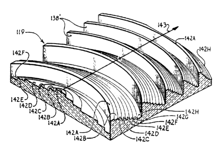
Figure 17 is an isometric view of a dispersive, Fresnel
microlens constructed in accordance with one embodiment of
the present invention. The microlens shown in Figure 17 has
a rectangular topology (is in the shape of a rectangle as
viewed in plan view), and the axis of the grating of the
prisms is not skewed with respect to the topology but is,
instead, aligned and parallel with the related sides of the
microlens. In Figure 17 a portion of the central part of one
end of the microlens has been broken away to show details of
structure.
Figure 18 is an elevation view, partly in cross section,
taken along the line and in the direction indicated by the
arrows 18-18 in Figure 17.
Figure 19 is an isometric view of another embodiment of
a dispersive Fresnel type microlens constructed in accordance
with the present invention. The microlens shown in Figure 19
has a rectangular topology, like the microlens shown in
Figure 17. The dispersive grating is perpendicular to the
direction arrow 143. The microlens shown in Figure 19
differs from the microlens shown in Figure 17 in the fact
that the microlens shown in Figure 19 is fabricated by a
binary fabrication process while the microlens shown in
Figure 17 is fabricated by a non-binary fabrication process.
Figure 20 is a side elevation view of a dispersive non
Fresnel microlens and shows, in diagrammatic fashion in the
lower part of the Figure, how the bandwidth of light existing
in the blur spot in the image plane is transmitted through
the dispersive microlens and is dispersed into individual
wavelengths or individual wavebands A, B and C at specific
locations on the detector plane.
Figure 21 is an isometric view showing specif is spectral
lines of the distributions (the intensity levels and the area
locations) of the dispersed wavelengths or wavebands on the
detector plane for a dispersive non-Fresnel microlens like
CA 02139108 2002-08-08
78585-3
1 t
8
that shown in Figure 20. Figure 21 shows, by the height of
the cones, the relative intensities of the specified
dispersed wavelengths; and Figure 21 shows, by the areas
occupied on the detector plane, the locations of the
dispersed wavelengths. The alignment of the locations of
the dispersed wavelengths shown in Figure 21 is a straight
line which is canted at an angle with respect to the
rectangular sides of the pixel shown in Figure 21. This
angle results from a corresponding angle of rotation of the
related grating of the related microlens. The total
bandwidth of the light transmitted through the dispersive
non-Fresnel microlens of Figure 20 is distributed within the
outer envelope indicated by the dashed outline in Figure 21;
and the wavelength separation is in fact a continuum, rather
than just the three separate cones shown for purposes of
illustration in Figure 21.
Figure 22 is an isometric view of a dispersive,
non-Fresnel, binary fabricated microlens constructed in
accordance with another embodiment of the present invention.
The microlens shown in Figure 22 has a topology which is
generally rectangular shaped, and the dispersion grating is
not rotated.
Figure 23 is an isometric view showing the
spectrum distributions (the intensity levels and the area
locations) of the dispersed wavelengths or wave bands on the
pixel in the detector plane for the dispersive, non-Fresnel,
binary microlens shown in Fig. 22. The bandwidth of light
in the blur spot at the microlens in the image plane is
dispersed to the smaller but elongated blur spot on the
detector plane, and the wavelengths in the elongated blur
spot in the pixel on the detector plane (as shown in Figure
23) are varied in a progressive way from one end of the blur
spot to the other end. As noted below with reference to
CA 02139108 2002-08-08
78585-3
,
9
Figures 35 and 36, the total energies that fall on each
detector area (within the total bandwidth) are obtained by a
convolution, or integration, of the spectral blur spots and
the responsivity function. The alignment of the dispersed
wavelengths or wavebands in Figure 23 is a straight line
which runs parallel to the sides of the pixel, and this
alignment is produced by a zero rotation of the dispersive
grating of the non-Fresnel microlens as shown in Figure 22.
Figures 24, 25 and 26 show the respective high
distribution (red), medium distribution (green) and low
distribution (blue) components existing in the elongated
pixel blur spot shown in Figure 23. It should be noted that
the terms red, green and blue are used here and throughout
the text to refer to the distribution in the waveband
discussed and not to specific colors as such.
Figure 24 is an isometric view showing only the
distribution (locations) and intensity levels of the longest
(in this case red) wavelengths in the elongated pixel plane
blur spot shown in Figure 23.
Figure 25 is an isometric view showing only the
distribution (locations) and intensity levels of the mid (in
this case green) wavelengths of the elongated pixel plane
blur spot shown in Figure 23.
Figure 26 is an isometric view showing only the
distribution (locations) and intensity levels of the
shortest (in this case blue) wavelengths of the elongated
pixel plane blur spot shown in Figure 23.
Figure 27 is a side elevation view of a
dispersive, Fresnel, non-binary microlens constructed in
accordance with another embodiment of the present invention
and shows, in diagrammatic fashion in the lower part of the
CA 02139108 2002-08-08
78585-3
figure, how the bandwidth of light existing in the blur spot
at the microlens in the image plane is transmitted through
the dispersive microlens and is dispersed into individual
wavelengths or individual wavebands C, B and A at specific
5 locations in a pixel on the underlying detector plane.
Figure 28 is an isometric view showing the
spectrum distributions (the intensity levels and the area
locations) of the dispersed wavelengths or wavebands on the
pixel in the detector plane for the dispersive, Fresnel,
10 non-binary microlens shown in Figure 27. The bandwidth of
light in the blur spot at the microlens in the image plane
is dispersed to the smaller but elongated blur spot on the
detector plane, and the wavelengths in the elongated blur
spot in the pixel on the detector plane (as shown in Figure
28) are varied in a progressive way from one end of the blur
spot to the other so that more than one wavelength can be
detected and/or located within the elongated blur spot on
the detector plane. The alignment of the dispersed
wavelengths or wavebands in Figure 28 is a straight line
which is rotated with respect to the sides of the pixel, and
this alignment is produced by a corresponding rotation axis
of the dispersive grating of the Fresnel, non-binary
microlens shown in Figure 27.
Figure 29, 30 and 31 show the respective red (high
distribution), green (medium distribution) and blue (low
distribution) components existing in the elongated pixel
blur spot shown in Figure 28.
Figure 29 is an isometric view showing only
distribution (locations) and intensity levels of the longest
(in this case red) wavelengths in the elongated pixel plane
blur spot shown in Figure 28.
CA 02139108 2002-08-08
78585-3
T
10a
Figure 30 is an isometric view showing only the
distribution (locations) and intensity levels of the mid (in
this case green) wavelengths of the elongated pixel
wavelengths of the elongated pixel plane blur Spot shown in
Figure 28.
Figure 31 is an isometric view showing only the
distribution (locations) and intensity levels of the
shortest (in this case blue) wavelengths of the elongated
pixel plane blur spots in Figure 28.
Figure 32A is a side elevation view of two side by
side dispersive, Fresnel, rotated dispersive grating,
microlenses formed directly on one surface of the substrate.
Each microlens is associated with three related detectors
located in a correspondingly rotated blur spot in a related
pixel on the opposite side of the substrate.
Figure 32B is a bottom plan view, taken generally
along the line and in the direction indicated by the arrows
32B--32B in Figure 32A. Figure 32B shows how the three
detectors are aligned in the pixel in the detector plane for
detecting the dispersed wavelengths or wavebands within the
elongated blur spot indicated by the dashed outline in
Figure 32B.
t ~ 94/00781 2 1 3 9 1 0 8 Y' per/ US93/06012
11
Figure 33 is a side elevation view, generally like
Figure 32A, but showing an embodiment in which two loop hole
detectors are used in each pixel. The non-binary, non-
Fresnel, dispersive microlenses shown in Figure 33 are
fabricated in silicon and are mated to a frontside-
illuminated detectors side as the loophole CdTe array.
Figure 34A is an enlarged elevation view in cross
section of one of the detectors of Figure 33.
Figure 34B is an isometric view of the detector shown in
Fig. 34A.
Figures 35 and 36 are related views showing how two sets
of detectors in a pixel in the detector plane can be
specifically sized and positioned to pick up two different
sets of signal information from the same overall color
dispersed information contained within the elongated blur
spot in the pixel in the detector plane. Figures 35 and 36
give a visual representation. The total energies that fall
on each detector area are obtained by a convolution, or
integration, of the spectral blur spots and the spectral
responsivity functions.
Figure 37 is a graph showing the information obtained
from the two different detectors positioned within an
elongated blur spot in a single pixel by a convolution of the
dispersed optical blur spot and detector responsivity
function.
Figure 38 is an isometric, fragmentary view showing an
array of non-dispersive, non-binary, Fresnel microlenses
which can be positioned in a peripheral part of the image
plane.
Figure 39 is an isometric view showing the spectral
distributions ( the intensity level and the area locations ) of
the wavelengths in the symmetrical spot formed on the
detector plane by a non-dispersive microlens like one of the
microlenses shown in Figure 38. Figure 39 illustrates how
the higher order harmonics (extending orthogonally outwardly
from the central cone for a square lens in Figure 39) produce
an Airy disk pattern. This orthogonal pattern can produce
resulting cross talk noise between adjacent pixels in the
detector plane: because the patterns can be aligned, and the
CA 02139108 2002-08-08
78585-3
12
harmonics from one pattern can extend into and can add to
the harmonics in an adjacent pixel.
Figure 40 is an isometric, fragmentary view like
Figure 39, but showing how an elongated blur spot formed in
the pixel plane by a dispersive microlens in the image plane
can also produce higher order harmonics in the pixel which
can extend orthogonally into and in alignment with harmonics
in adjacent pixels to produce cross talk noise.
Figure 41 shows how a diagonally rotated
dispersion grating angle can result in a diagonal alignment
of higher order harmonics which can still result in cross
talk noise between diagonally adjacent pixels in the pixel
plane.
Figure 42 shows a topology for square microlenses
with a diagonal rotation angle of the dispersion grating
which is effective to eliminate orthogonal cross talk noise
but which can still result in diagonal cross talk noise
between diagonally adjacent pixels.
Figure 43 shows a topology in which rectangular
shaped microlenses, each having a diagonal rotation angle of
the dispersion grating, can be longitudinally offset or
staggered in adjacent rows to eliminate any diagonal cross
talk noise between diagonally adjacent pixels in the
detector plane.
Figures 44, 45, 46 and 47 show configurations for
microlenses.
Figure 44 shows a rectangular configuration.
Figure 45 shows a rhombic, trapezoidal
configuration.
CA 02139108 2002-08-08
78585-3
13
Figure 46 shows a hexagonal configuration. This
configuration has a number of advantages for maximizing the
concentration and distribution of information in a related
detector plane.
Figure 47 shows a circular configuration for a
microlens.
Figure 48 shows a microlens array in which the
individual microlenses are circular microlenses.
Figure 49 shows a microlens array in which the
individual microlenses have a rhombic configuration.
Figure 50 shows a microlens array in which the
individual microlenses have a hexagonal configuration.
Figure 51 shows a microlens array in which each
individual microlens has a rectangular configuration and in
which each microlens in each row is offset with respect to
the microlenses in adjacent rows.
Figure 52 is an elevation view of a rectangular,
Fresnel, binary, dispersive microlens constructed in
accordance with an embodiment of the present invention.
Figure 53 is a diagrammatic plan view of the
microlens shown in Figure 52 and shows the dispersion
grating having a zero rotation angle (as indicated by the
direction arrow 143 which is perpendicular to the grating).
Figure 54 is a top plan photograph (generated by a
scanning electron microscope -- SEM) of the fabricated
dispersive microlens shown in Figures 52 and 53.
Figure 55 is a top plan SEM photograph showing a
fabricated array of microlenses made up of individual
CA 02139108 2002-08-08
78585-3
14
microlenses each having the construction shown in Figure 54.
Figure 56 is a diagrammatic plan view, like Figure
53, but showing a rectangular microlens having the
dispersion grating rotated at an angle perpendicular to the
direction arrow 143 in Figure 56.
Figure 57 is a top plan SEM photograph of the
fabricated dispersive microlens shown in Figure 56 and
embodying the Fresnel, binary construction shown in Figure
52.
Figure 58 is a top plan view of four pixels in a
detector plane, offset in adjacent rows, to correspond to
the offset of related rectangular microlenses like the
microlens shown in 57, and showing the location of the
elongated blur spot in each pixel as produced by the
microlens construction shown in Figure 57.
Figure 59 is an isometric view of a dispersive,
Fresnel microlens like that shown in Figure 57. Figure 59
shows a dispersive, rectangular-shaped, binary fabricated,
Fresnel microlens having the dispersion grating rotated at
the angle indicated by the direction arrow in Figure 59.
Figure 60 is an isometric view (similar to Figure
21) showing specific spectral lines of the distributions
(the intensity levels and the locations) of dispersed
wavelengths on the pixel in the detector plane for the
dispersive, Fresnel, binary microlens shown in Figure 59.
As noted above with reference to Figure 21, the illustrated
spectral blur spots are typical (blue, green, red) and are
related to the lambda-low to lambda-high continuum within
the total bandwidth (indicated by the dashed outline in
Figure 60).
CA 02139108 2002-08-08
78585-3
f
Figure 61 is a schematic plan view showing a
hexagonal shaped microlens having a dispersion grating
inclined at the angle indicated by the direction arrow in
Figure 61.
5 Figure 62 is a plan SEM photograph of a fabricated
low dispersive, binary, Fresnel, hexagonal shaped microlens
having the dispersion grating inclined at the angle
indicated in Figure 61.
Figure 63 is a top plan SEM photograph of a
10 fabricated test array of hexagonal shape microlenses having
the structure of the microlens shown in Figure 62.
Figure 64 is a fragmentary, plan view showing a
rhombic shaped microlens having a dispersion grating rotated
at the angle perpendicular to the direction arrow in Figure
15 64.
Figure 65 is a top plan SEM photograph of a
fabricated high dispersive, hexagonal shaped, binary
fabricated, Fresnel microlens having a dispersion grating
rotated at the angle perpendicular to the direction arrow
143 in Figure 64.
Figure 66 is a top plan view of a composite array
of pixels located at the detector plane and comprising a
high resolution, (multicolor) pixel array of hexagonal
shaped pixels in the central part of the composite array and
having a lower resolution (wideband) pixel array of pixels
in the peripheral part of the array. It should be noted
that the use of multicolor and/or wideband may be a
particular choice for a particular application. The high
resolution region in combination with a low resolution
region is often a more fundamental issue.
CA 02139108 2002-08-08
78585-3
15a
Figure 67 is an isometric, fragmentary, enlarged
view showing a composite array of microlenses in an image
plane for association with the composite array of pixels
shown in Figure 66. High resolution, dispersive, hexagonal
microlenses comprise the central part of the composite
microlens array; and non-dispersive, low resolution,
wideband microlenses make up the outer peripheral part of
the composite microlens array.
Figure 68 is an elevation view showing how three
emitters (each emitting a specified wavelength of color --
red, green and blue) are arranged in alignment within an
axially rotated, elongated blur spot in a pixel in the pixel
plane and are associated with a related, same rotation angle
of dispersive grating, microlens in an image plane for
combining the three separate wavelengths or wavebands of
light emitted by the three emitters into a bandwidth of
light at a blur spot existing at the location of the
dispersive microlens in the image plane. The color content
and intensity in the bandwidth of the light in the blur spot
at the microlens are dependent upon the relative intensities
of the different wavelengths emitted by the three emitters
in the detector plane.
Figure 69 is a bottom plan view taken along the
line and in the direction indicated by the arrows 69-69 in
Figure 68.
Figure 70 is a diagrammatic view showing how the
dispersive lens of the present invention is used in one
(color combining) mode for combining a plurality of
different, emitted wavelengths (emitted from emitters in an
emitter plane) into a bandwidth of the wavelengths (at a
blur spot in an image plane) and is used in another (color
CA 02139108 2002-08-08
78585-3
15b
detecting) mode for detecting multiple different wavelengths
(by detectors at a detector plane) from a bandwidth of
wavelengths (existing within an image plane blur spot) so as
to enable color information not only to be emitted and
combined but also to be dispersed and detected for color
transmitting and regenerating methods and apparatus, such
as, for example, color television, color recording, color
facsimile and color printing processes and apparatus.
DETAILED DESCRIPTION OF THE PREFERRED EMBODIMENTS
The present invention relates to dispersive
microlens apparatus and methods which can be used in a
detecting mode for dispersing and detecting multiple
different wavelengths or wavebands from a bandwidth of the
wavelengths existing within an image plane blur spot and
which can also be used
WO 94/00781 ~ ~ ~ ~ ~ 16 PCT/US93/06012
in a combining mode (for combining a plurality of different,
emitted wavelengths into a bandwidth of the wavelengths at a
blur spot in an image plane).
Figures 1 and 2 of the drawings illustrate object
imaging environments in which the dispersive microlens
apparatus and methods of the present invention are utilized
to perform complex object imaging and analysis operations.
Figures 68, 69 and 70 of the drawings illustrate color
combining environments in which the dispersive microlens
apparatus and methods of the present invention are used for
combining a plurality of different, emitted wavelengths into
a bandwidth of wavelengths at a blur spot in an image plane.
Figure 70 illustrates how the dispersive microlens
apparatus and methods enable color information not only to be
dispersed, separated and detected but also to be emitted and
combined for color transmitting and regenerating
applications, such as, for example, color television, color
recording, color facsimile and color printing processes and
apparatus.
The use of the dispersive microlens in the first mode
(the mode for detecting multiple different wavelengths or
wavebands from a bandwidth of the wavelength) will be
described first and will be described with reference to use
in a sensor environment of the general kind shown in~Figures
1 and 2.
Figure 1 shows a sensor system, indicated generally by
the reference numeral 101, which can be used for
imaging/detecting an object and which can also provide (by
use of the dispersive microlens apparatus and methods of the
present invention) real time discrimination of sensed optical
information for certain other qualities, such as, for
example, color and/or temperature, of the object or objects
generating the optical information.
The sensor system 101, as illustrated in Figure 1,
includes imager optics 109, focal plane arrays 111
(comprising microlens arrays and detector arrays), and a
signal processing unit 113.
Figure 2 is a diagrammatic view showing how each of
three adjacent microlens 119 has an individual instantaneous
' 94/00781
._, _ k ., PCT/US93/06012
17
f field of view ( IFOV-1, IFOV-2 and IFOV-3 ) and showing how the
energy (or object) in that individual IFOV is transmitted to
the detectors (124A and 124B) associated with the particular
microlens.
Figure 3 is an enlarged, diagrammatic view which
illustrates details of the focal plane arrays 111 shown ire
Figures 1 and 2.
The focal plane arrays 111 in Figure 3 comprise a
microlens array 115 in an image plane and a pixel array 11'~
in a detector plane.
The use of the microlens array 115 at the image plane in
the focal plane arrays 111 allows the concentration of
incident irradience to a small fraction of the pixel area in
the detector plane.
As illustrated in Figure 3 (and as shown in more detail
in the fragmentary enlarged Figure 67 view), the microlens
array 115 (in one embodiment of the invention) is a composite
array which comprises a central (foveal vision) array of high
resolution, dispersive, individual microlenses 119 surrounded
by an outer, peripheral array of non-dispersive, low
resolution, wideband, individual microlenses 121. In other
embodiments, different combinations of high and low
resolution regions may be used and different combinations of
dispersive and non-dispersive microlens may be used.
The pixel array 117 contains a plurality of pixels with
each individual pixel related to a corresponding individual
microlens in the microlens array 115.
Thus , in the specific embodiment shown in Figure 3 , high
resolution (multicolor) pixels 123 are located in the central
part of the composite pixel array 117 and lower resolution
(wideband) pixels 126 are located in the peripheral part of
the composite pixel array 117.
As best illustrated in Figures 2, 3, 6 and 7, an
instantaneous field of view (IFOV), and any object or objects
within that instantaneous field of view, are imaged into an
individual blur spot 125 at the location of an individual
microlens 119 at the image plane. The optical information
within this blur spot is transmitted through the microlens
WO 94/00781 213 910 8 18 P~T/US93/0601
119 to a related pixel 123 in the detector plane. (See
Figure 2.)
As will be described in greater detail below, one or
more detectors 124 (see Figures 2, 4A, 4B, 4C, 7, 8A, 8B, 9
and 10) are positioned within each pixel in the detector
plane for receiving a signal or signals from the reduced size
pixel blur spot.
Figures 4A, 4B and 4C are enlarged, fragmentary views,
partly in cross section, showing how multiple detectors are
associated with non-Fresnel dispersive microlenses (Figure
4A) and Fresnel dispersive microlenses (Figure 4B) and
showing how a single detector is associated with a wideband
Fresnel, non-dispersive microlens (Figure 4C).
It is desirable not to have any dead space in the focal
plane arrays 111, for reasons which can best be understood by
reference to Figure 5.
Figure 5 shows a detector plane used without an
associated micro-optics array. An object 127 within a blur
spot 125 which falls substantially fully upon a related
detector 124 would have substantially all of the energy and
information within that object transmitted to a corresponding
component in the signal processing unit 113; so a dead zone
between adjacent detectors would not have too much
significance with respect to the object 127.
However, if (in the previously used Figure 5, detector-
only, focal plane array) an object 129 spans several adjacent
detectors 124 and also is disposed above dead zones between
the microlenses (as indicated by the double cross-hatched
portion 131 of the object image 129 in Figure 5), then that
portion of the object image 129 (which does not fall onto any
detector 124) would not be transmitted to the signal
processing unit 124 and would be lost.
The present invention includes micro-optics above the
detector plane array. As will be more clear from the
description to follow, this use of the microlenses permits
the detectors to be spaced apart from one another without any
problems of dead zone losses as described immediately above
in reference to the previously used Figure 5 detector array
construction.
CA 02139108 2002-08-08
78585-3
19
The preferred construction is to have all of the
microlenses in the microlens array immediately adjacent one
another so as not to have any optically dead space between
any of the microlenses.
Figure 6 shows such construction for square shaped
(in plan), Fresnel-type microlenses 121.
Figure 6 and related Figure 7 illustrate how all
of the optical information within each individual blur spot
125 is preserved and is transmitted to detectors 124 in
pixels 123 in the detector plane, even when a blur spot
spans more than one individual microlens in the microlens
array 115.
Thus, for example, the object image 129 which
falls on four adjacent microlenses 121 (in Figure 6) is
fully transmitted to four detectors 124 in the four related
pixels 123 (see Figure 7) in the detector plane.
All of the energy is conserved.
It should also be noted that each individual
microlenses, in the course of transferring the optical
information at an image plane blur spot into a smaller
detector plane blur spot in a related pixel in the detector
plane, is effective to produce a high contrast ratio, high
fill factor and high optical gain of the optical information
in the detector plane blur spot with respect to any
existing, unwanted noise (produced by large detector
elements) which may be present at the detector plane.
The optical gain achieved is the area ratio of the
microlens to the detector (see Figure 8A).
CA 02139108 2002-08-08
78585-3
19a
The microlens array 115 and pixel array 117
provide high overall optical efficiency, nearly 100% fill
factor, extended wavelength response and reduced detector
noise levels.
Microlenses constructed in accordance with the
present invention may typically range in size from a
diameter D of 50 microns to 1000 microns, and the related
detectors may be fabricated from bulk material that is
thinned to a thickness t that represents an f/1 lens.
Because the microlenses transfer the optical
information in the image plane blur spots into respective
smaller detector plane blur spots in respective detector
plane pixels, the small detector plane blur spots
(corresponding
WO 94/00781 213 9 ~ Q ~ 20 P~'/US93/0601:
generally to the diameter d of the detector 124 shown in
Figure 8A) leave relatively large adjacent areas, or real
estate, in the detector plane which can be used for other
purposes.
As shown in Figure 8A and 8B, micro cooling channels 133
can be positioned in the relatively large adjacent areas and
used for cooling nearby structure.
The available real estate may also be utilized for
analog signal processing circuits, such as, for example, the
analog circuits 126 in Figures 8A and 8B. As will be
described in more detail below, the circuits can be
conventional detector read-out circuits, detector signal
adding circuits or ratio-ing circuits, as the system design
requires.
As also indicated by Figure 8A, and as will be described
in more detail below, multiple detectors, such as the
detectors 124A, 124B and 124C shown in Figure 8B, can be
positioned in a number of locations and in a variety of
alignments within each individual pixel. Having the space
available to do this in a detector plane pixel is a benefit
which is of particular utility in connection with a
dispersive microlens like the dispersive, high resolution
microlens 119 shown in Figure 8B, as will be described in
more detail below.
Figure 9 is a fragmentary plan view which shows how two
detectors 124A and 124B can be positioned (in this case
orthogonally) in each unit pixel 123.
Figure 10 is a fragmentary top plan view showing how
three detectors 124A, 124B and 124C may be positioned within
each unit pixel 123.
It should be noted that the blur spot 125 results from
a combination of refraction and diffraction. The blur
resulting from refraction ( geometric optics ) results from the
different focus of different wavelengths. The blur caused by
diffraction (wave optics) is inherent to a certain degree in
all refractive (geometric optics) lenses. This blur spot
phenomenon which results primarily from refraction (geometric
optics) and, to a much lesser extent, diffraction (wave
optics) of lenses is described at pages 727 and 728 of
CA 02139108 2002-08-08
78585-3
f
21
Physics by Hausmann and Slack, 3rd edition, 1948, and
published by D. Van Nostrand Company, Inc., New York.
In accordance with the present invention, a
microlens (1) is constructed to transmit a selected
bandwidth of light existing in the incident blur spot at the
microlens plane 115 to a smaller pixel blur spot in a pixel
plane 117 spaced at a selected distance from the microlens
and (2) includes dispersion means for producing both a
controlled dispersion of the bandwidth of light (as the
light is transmitted to the smaller blur spot) and also an
elongated shape of the smaller pixel blur spot (in which the
elongated shape wavelengths or wavebands are varied in a
progressive way from one end of the elongated blur spot to
the other so that more than one wavelength can be detected
and/or located within the elongated blur spot).
The dispersion means comprise a configured surface
formed integrally on the microlens.
Figures 11, 12 and 13 are related views showing
how a dispersion producing surface configuration (Figure 11)
can be visualized as being combined with a plano convex
surface configuration microlens (Figure 12) to form a
single, combined surface, dispersive non-Fresnel microlens
(Figure 13) in accordance with one embodiment of the present
invention.
As illustrated in Figure 11 the dispersion
producing means 135 may be visualized as a series of
identically sized, identically spaced, individual prism
surfaces each having an inclined surface 136 and a vertical
surface 138. The prism surfaces are aligned in a grating
arrangement (an arrangement in which corresponding surfaces
CA 02139108 2002-08-08
78585-3
21a
on corresponding prisms extend parallel to one another).
The prism surfaces are effective to produce dispersion
substantially entirely by geometric refraction (and not to
any significant extent by the wave optics diffraction of a
diffraction grating).
The grating arrangement shown in Figure 11 is a
grating in the general sense of the term. That is, the
arrangement of the prismatic surfaces, when viewed from
above, can have
WO 94/00781 213 91 ~ ~ PCT/US93/0601~
22
the appearance of parallel elements, like a grating of
latticed bars set in a window, door, etc. The use of the
term grating with reference to the construction shown in
Figure 11 is not a reference to a grating as an optical
diffraction grating. The grating shown in Figure 11 does not
produce slits equally spaced which can cause dispersion by
spreading of a wave into its component frequencies. The
grating arrangement shown in Figure 11 instead essentially
causes dispersion of the light by causing different
wavelengths of the light to be transmitted through the
material of the microlens at dif f erent velocities . There is ,
of course, always some diffraction which is caused by the
material of the lens itself. In this regard, see the above
discussion of the formation of the blur spot 125 and the
reference to pages 727 and 728 of Physics by Hausmann and
Slack.
Figure 12 shows a plano convex microlens 137 having a
convex surface 140.
When the dispersion surface means 135 shown in Figure 11
are combined with a plano convex surface microlens 137 shown
in Figure 12 a dispersive microlens 119 shown in Figure 13 is
obtained. The curved surfaces 142 of the dispersive
microlens 119 have curvatures which are a combination of the
curvature 140 of Figure 12 and the inclination of the
prismatic surfaces 136 shown in Figure 11.
The surfaces 138 shown in Figure 13 correspond to the
surfaces 138 shown in Figure 1l for producing the prism
ef f ects .
Figures 14, 15 and 16 are related views showing how a
dispersion producing surface configuration 135 ( Figure 14 ) is
associated with a Fresnel-type plano convex microlens 139
(Figure 15) to form a dispersive Fresnel microlens 119
(Figure 16) in accordance with another embodiment of the
present invention.
The dashed lines shown in Figure 16 are included just to
represent the amount of material which is eliminated thus
resulting in a thinner wafer when the lens is fabricated in
a Fresnel structure rather than in a non-Fresnel structure.
CA 02139108 2002-08-08
78585-3
23
Figure 17 is an isometric view of a dispersive,
Fresnel microlens 119 constructed in accordance with one
embodiment of the present invention.
The dispersive microlens 119 shown in Figure 17 is
basically like the lens shown in Figure 16 but is shown (in
Figure 17) mounted on a substrate 141.
The substrate 141 may be a separate material if
required for a particular optomechanical application, or the
substrate 141 may be common for the lenses on one side and
the detectors on the other side (back illuminated
detectors ) .
The microlens 119 shown in Figure 17 has a
rectangular topology (is in the shape of a rectangle as
viewed in plan view), and the grating is not rotated with
respect to the topology but is instead, aligned and parallel
with the related sides of the microlens. In Figure 17 a
portion of the central part of one end of the microlens has
been broken away to show details of structure.
Figure 18 is an elevation view, partly in cross
section, and is taken along the line and in the direction
indicated by the arrows 18-18 in Figure 17.
The dispersive, Fresnel microlens shown in Figure
17 is fabricated by non-binary techniques.
Figure 19 shows a dispersive, Fresnel microlens
having a rectangular, square topology and a non-rotated
grating angle (all similar to the microlens shown in Figure
17), but the microlens 119 shown in Figure 19 is fabricated
by a binary fabrication process.
CA 02139108 2002-08-08
78585-3
23a
The angle of the dispersive grating is
perpendicular to the direction arrow 143 in Figure 19.
Figure 19 shows, in the dashed outline beneath the
direction grating arrow 143, the cross section configuration
of the Fresnel-type dispersive microlens in that part of the
microlens.
As illustrated in Figure 19, the vertical wall
surfaces 138 which form part of the dispersion grating are
curved surfaces (as viewed in plan) rather than straight
lines.
Because the dispersive microlens 119 is
constructed by binary fabrication, the surfaces 142 are not
smoothly curved (like the smoothly curved surfaces 142 shown
in Figure 17)
WO 94/00781 PCf/LJS93/0601
24
but are instead formed as a series of discrete levels 142A,
142B, 142C, 142D, 142E and 142F. The number, n, of discrete
levels produced is a function (n=2") of the number, M, of
photolithographic and anisotropic etching steps (Number of
Masks) involved in the fabrication. Note that 2" is the
definition of binary as a number. The number of levels
determines the smoothness to which the surface can be
approximated and, consequently, its efficiency.
As noted above, the dispersive microlens of the present
invention transmits a selected bandwidth of light (existing
in the incident blur spot 125 at the microlens ) to a much
smaller pixel blur spot in a plane space at a selected
distance from the microlens. This much smaller pixel blur
spot is indicated in Figure 20 by the reference numeral 145.
In Figure 20 the blur spot 145 is shown, for easier viewing,
larger than and out of scale to the actual ratio of diameters
D (at the image plane) to d (at the detector plane).
The dispersive means on the microlens produce both a
controlled dispersion of the bandwidth of the light (as the
light is transmitted to a smaller pixel blur spot) and also
an elongated shape of the smaller pixel blur spot. The
wavelengths or wavebands in the elongated pixel blur spot are
varied in a progressive way from one end of the elongated
blur spot to the other so that more than one wavelength can
be detected and/or located within the elongated blur spot.
Figures 20 and 21 illustrate how the bandwidth of light
existing in the blur spot 125 ( see Figure 6 )' at the microlens
119 in the image plane is transmitted (see the illustrative
light rays indicated by the dashed lines in Figure 20)
through the dispersive microlens and is dispersed into
individual wavelengths or wavebands 145A, 145B and 145C
within the elongated detector plane blur spot 145 at specific
locations on the detector plane.
Figure 21 is an isometric view showing selected
wavelengths from the spectrum distributions (the intensity
levels and the area locations) of the dispersed wavelengths
or wavebands 145A, 145B and 145C on the detector plane pixel
123 for a dispersive, non-Fresnel microlens like that shown
in Figure 20. Figure 21 shows, by the height of the cones
CA 02139108 2002-08-08
78585-3
145A (blue), 1458 (green) and 145C (red), the relative
intensities of the dispersed wavelengths or wavebands.
As noted above in the description, the use of the
terms blue, green and red is a use to indicate the low,
5 medium and high wavelengths from the spectral band existing
in the blur spot. The use of the terms is not intended to
refer to specific, visible colors as such.
Figure 21 shows, by the areas occupied (by the
basis of the cones 145A, 1458 and 145C) on the detector
10 plane, the locations of the dispersed wavelengths or
wavebands. The alignment of the locations of the dispersed
wavelengths or wavebands 145A (blue), 1458 (green), and 145C
(red) shown in Figure 21 is a straight line which is canted
at an angle with respect to the rectangular sides of the
15 pixel 123 shown in Figure 21. This angle results from a
corresponding angle of rotation of the related grating of
the related microlens 119 shown in Figure 20.
Figure 22 is an isometric view of a dispersive,
non-Fresnel binary fabricated microlens constructed in
20 accordance with another embodiment of the present invention.
The microlens 119 in figure 22 has a topology which is
generally square shaped, and the axis of the dispersion
grating is aligned with the sides of the microlens so that
there is no rotation to this axis. The dashed lines in
25 Figure 22 show the cross sectional configuration of the
microlens at the locations of the dashed lines.
Figure 23 is an isometric view showing the
spectrum distributions (the intensity levels and the area
locations) of the dispersed wavelengths or wavebands on the
pixel 123 in the detector plane for the dispersive, non-
CA 02139108 2002-08-08
78585-3
26
Fresnel, binary microlens 119 shown in Figure 22. The
bandwidth of light in the blur spot 125 at the location of
the microlens 119 in the image plane is dispersed to the
smaller but elongated blur spot 145 on the detector plane.
The wavelengths in the elongated blur spot 145 in the pixel
123 on the detector plane (as shown in Figure 23) are varied
in a progressive way from one end of the pixel plane blur
spot to the other so that more than one wavelength can be
detected and/or located within the elongated blur spot 145
on the detector plane. The elongated blur spot is dispersed
into the respective components 145A (blue), 145B (green),
and 145C (red) components as shown in Figure 23. The
alignment of the dispersed wavelengths or wavebands of the
pixel plane blur spot 145 in Figure 23 is a straight line
which runs parallel to the sides of the pixel 123, and this
alignment is produced by a zero angle rotation of the
dispersive grating on the non-Fresnel microlens 119 shown in
Figure 22.
Figures 24, 25 and 26 show the respective red,
green and blue components existing in the elongated pixel
plane blur spot shown in Figure 23.
Figure 24 is an isometric view showing only the
distribution (location) and intensity levels of the longest
(in this case red) wavelengths in the elongated pixel plane
blur spot shown in Figure 23.
Figure 25 is an isometric view showing only the
distribution (location) and intensity levels of the mid (in
this case green) wavelengths in the elongated pixel plane
blur spot shown in Figure 23.
CA 02139108 2002-08-08
78585-3
26a
Figure 26 is an isometric view showing only the
distribution (locations) and intensity levels of the
shortest (in this case blue) wavelengths of the elongated
pixel plane blur spot shown in Figure 23.
Figure 27 is a side elevation view of a
dispersive, Fresnel, non-binary, rotated grating axis,
microlens 119 constructed in accordance with another
embodiment of the present invention.
Figure 28 is an isometric view (generally similar
to the isometric view shown in Figure 23) showing the
spectrum distributions (the intensity levels and the area
locations) of the dispersed wavelengths or wavebands 145A
(blue), 145B (green), and 145C (red) which make up the
elongated pixel plane blur spot 145 produced by the
microlens 119 shown in Figure 27. The alignment of the
dispersed wavelengths or wavebands in Figure 28 is a
straight line which is rotated with respect to the sides of
the pixel 123, and this alignment is produced by a
corresponding rotation axis of the dispersive grating of the
microlens 119 shown in Figure 27.
94/00781 213 9 ~ 0 g PCT/US93/06012
27
Figures 29 , 30 and 31 show the respective red, green and
blue components existing in the elongated pixel plane blur
spot 145 shown in Figure 28.
There are a number of ways which the dispersive
microlens 119 and associated detectors 124 can be structured
in accordance with the present invention.
Figures 32A and 32B show one way, and Figures 33, 34A
and 34B show another way.
In the construction shown in Figures 32A and 32B,
dispersive, Fresnel, skewed dispersive grating, microlenses
119 are formed directly on one surface of a commercially
available cadmium tellurium (CdTe) substrate 147.
Figure 33 shows how a dispersive, non-Fresnel,
microlenses 119 fabricated in silicon (Si) is mated to a
frontside-illuminated, commercially available, loophole array
of two CdTe detectors 124A and 124B in each pixel plane blur
spot 145.
As illustrated in Figure 33, one detector 124A can be
used to detect one bandwidth of colors in the elongated pixel
plane blur spot 145 and another detector 124B can be used to
detect another, different bandwidth of colors within the
elongated pixel plane blur spot 145.
This positioning and selection of multiple detectors to
detect multiple signals from the single, elongated pixel
plane blur spot 145 will be described in more detail below
with reference to Figures 35 and 36.
Because the dispersive microlens of the present
invention disperses the component wavelengths or wavebands of
light within the elongated pixel plane blur spot 145 in a
progressive way and at exact locations in the pixel plane
blur spot, a plurality of detectors can be positioned at
particular locations within the elongated blur spot to detect
specif is signals which are dependent upon the locations of
the detectors in the pixel plane blur spot. This feature of
the present invention is best illustrated in Figures 35 and
36.
Figures 35 and 36 are related views showing how two sets
of detectors in a pixel 123 in the detector plane can be
specifically sized and positioned to pick up two different
WO 94/00781 PC'1'/US93/0601:
2139148 2$
sets of signal information from the same overall color
dispersed information contained within the elongated blur
spot 145 in the pixel 123 in the detector plane. The
particular selection chosen is system dependent.
The uses of the two sets of detectors illustrated in
Figures 35 and 36 permit the pick-up of two different sets of
signal information from the long, medium and short
wavelengths within any given bandwidth. In the particular
example illustrated in Figures 35 and 36 the illustrated band
is long wavelength infrared (LWIR) in the 8-12 micron
bandwidth.
This 8-12 LWIR is an example. Similar results may be
generated in other wavelength bands , i . a . , visible ( Vis ) near
infrared (NWIR), short infrared (SWIR), mid infrared (MWIR)
region.
Figure 35 shows how one detector 124A is sized and
positioned to pick up a signal which is representative of the
energy contained within both the 145C (red, 12 micron)
wavelength and the 145B (green, 10 micron) wavelength while
the other detector 124B is sized and positioned to pick up a
signal which is representative of the energy primarily within
the 145A (blue, 8 micron) wavelength of the elongated
detector plane blur spot 145.
In Figure 35 the dispersive microlens which produces the
elongated blur spot 145 is a 100 micrometer square, Fresnel
microlens having a rotated grating which is rotated to an
angle of 14 degrees (perpendicular to the line indicated by
the direction arrow 143). Grating rotation/canting angle is
selected from a design requirement to minimize optical cross
talk between neighboring pixels. The microlens was
fabricated by a binary fabrication process utilizing two
photolitho-graphic and anisotropic etching steps. The
resulting blur spot 145 shown in Figure 35 is basically like
that illustrated in Figure 28 of the drawings.
Figure 36 shows how a different set of signals can be
obtained (from the same pixel plane blur spot as shown in
Figure 35) by using a set of detectors which are positioned
at locations different from the set of detectors shown in
Figure 35.
94/00781 ~ ~ 3 9 I 0 g " PCT/ S93/0
.... U 6012
2~
In Figure 36 the detector 124A is sized and positioned
to pick up a signal which represents all of the energy
contained within the 145C portion (the red, 12 micron)
wavelength and part of the energy contained within the longer
wavelength end of the 145B portion ( the red-green, 11 micron )
wavelengths. The other detector 124B is positioned to pick
up a signal which is representative of all of the information
contained within the portion 145C (the blue, 8 micron)
wavelength and a part of the 145B portion (the green, 9 to l0
micron) wavelengths. Thus, the detector 124B picks up a
signal which represents the energy contained within the 10 to
8 micron waveband and the detector 124A picks up the energy
contained in the 12 to 11 waveband in the Figure 36
positioning of the two detectors.
Other topologies, detector layouts, size selection,
fabrication techniques and Fresnel/non-Fresnel selections can
be used for other, specific applications.
Figure 37 is a graph which illustrates how two different
detectors positioned within a single elongated blur spot in
a single pixel ( see Figure 33 ) provide multiple signals which
can be used to obtain highly effective information with
regard to objects imaged within the blur spot at the
dispersive microlens.
The detectors in each pixel can be summed in the
acquisition mode to obtain an increased signal.
In the discrimination mode the color contrast is
evaluated to determine the object temperature.
The ratio of the energies are also used as a temperature
discriminator.
The present invention recognizes the possible problem of
cross talk noise between adjacent pixels in the detector
plane and provides a number of constructions and arrangements
for minimizing or eliminating such cross talk noise.
How this problem of possible cross talk noise can
develop will now be discussed with reference to Figures 39,
40, 41, 42 and 43.
Figure 39 shows the pixel plane blur spot 125 formed
within a pixel 126 by a single, non-dispersive, wideband
CA 02139108 2002-08-08
78585-3
microlens (such as, for example, a single microlens 121
shown in Figure 38).
Figure 39 shows how the blur spot 125 has higher
order harmonics 125-1, 125-2, 125-3, etc. (extending
5 orthogonally outwardly from the central cone in Figure 39).
This produces an Airy disk pattern when the microlens is a
simple, wideband, non-dispersive lens like a microlens 121
shown in Figure 38. This orthogonal pattern can produce
resulting cross talk noise between adjacent pixels in the
10 detector plane because (depending on how the microlenses and
pixels are aligned in the respective arrays) the noise
patterns can be aligned and the harmonics from one pattern
in one pixel can extend into and can add to the harmonics in
an adjacent pixel.
15 Figure 40 shows how an elongated blur spot 145
formed in a pixel 123 in the pixel plane by a dispersive
microlens in the image plane can also produce higher order
harmonics which can extend orthogonally into and in
alignment with harmonics in adjacent pixels to produce cross
20 talk noise. The higher order harmonics are illustrated but
are not numbered in Figure 40.
Figure 41 shows how a diagonally rotated
dispersion grating angle (a grating perpendicular to the
arrow 143) can result in a diagonal alignment of higher
25 order harmonics which can still result in cross talk noise
between diagonally adjacent pixels 123 in the pixel plane,
even though the transverse higher order harmonics (indicated
by the direction arrows 149 in Figure 41) are laterally
offset from one another between adjacent pixels 123.
CA 02139108 2002-08-08
78585-3
30a
Figure 42 shows a topology for rectangular
microlenses with a diagonal rotation angle (perpendicular to
the direction arrow 143) of the dispersion grating which is
effective to eliminate orthogonal cross talk noise (in the
direction indicated by the arrows 149 in Figures 41 and 42)
but which can still result in diagonal cross talk noise (in
the direction indicated by the direction arrow 143) between
diagonally adjacent pixels.
Figure 43 shows a topology in which rectangularly
shaped microlenses, each having a diagonal rotation angle
(perpendicular
21~91~
~ 94/00781 PCT/US93/06012
31
to the direction arrow 143) of the dispersion grating, can be
longitudinally offset or staggered in adjacent rows to
eliminate any diagonal cross talk noise between diagonally
adjacent pixels in the detector plane.
Figures 44 through 51 illustrate topologies and
arrangements of arrays of microlenses which may be used in
the present invention.
Two basic features are thus available, in accordance
with the present invention, for optimizing a construction to
eliminate or to modulate signal to noise. The two features
are topology (pixel shape) and grating orientation. By
combining these two features in a specific way for a specific
application the signal to noise can be optimized.
Figures 44, 45, 46 and 47 show respective square,
rhombic, hexagonal and circular configurations for
microlenses. Any and all of these configurations may
incorporate dispersive means so that the microlenses are
dispersive microlenses 119 rather than wideband, non
dispersive microlenses. Any and all of these configurations
can also be used for wideband, non-dispersive microlenses.
The various configurations of the individual microlenses
shown in Figures 44-47 can be arranged in the various arrays
shown in Figures 48-51.
In addition, as illustrated in Figure 67, composite
arrays (which contain combinations of microlens shapes and
features) can be utilized to obtain specific, desired
results.
Figures 52-55 illustrate how a square, Fresnel, binary
fabricated, dispersive microlens 119 having a zero skew angle
grating (perpendicular to the arrow 143 in Figure 53) is
assembled in a high resolution microlens array (see Figure
55) with individual microlenses offset in adjacent rows (see
Figure 55). As noted above Figures 54 and 55 are photographs
of a fabricated microlens and a fabricated microlens array.
The photographs were generated by a scanning electron
microscope -- SEM.
Figures 56-58 are related views showing how a
dispersive, Fresnel-type, binary fabricated, microlens 119
like that shown in Figure 52, but having a skewed grating
CA 02139108 2002-08-08
78585-3
32
angle (perpendicular to the arrow 143) as illustrated in
Figure 56, and arranged in longitudinally offset
relationship in adjacent rows, produces offset blur spots
145 in the related pixels 123 in the pixel plane so as to
minimize or to totally eliminate cross talk noise between
both laterally and diagonally adjacent pixels.
Figure 59 is an isometric view of a dispersive,
Fresnel microlens like the microlens shown in Figure 57.
Figure 59 shows a dispersive, square shaped, binary
fabricated, rotated angle grating, Fresnel microlens having
the dispersion grating rotated at the angle perpendicular to
the direction arrow 143 in Figure 59.
Figure 60 is an isometric view showing the
spectrum distribution (the intensity levels and the
locations) of the dispersed wavelengths or wavebands 145A,
145B and 1450 in the pixel blur spot on the pixel 123 as
produced by the microlens 119 shown in Figure 59. Figure 60
shows, in isometric view, the pixel blur spot locations and
alignments (which are also shown in Figure 58).
Figures 61, 62 and 63 show how low spectral
resolution, dispersive hexagonal shaped, Fresnel-type,
binary fabricated, microlenses (having the dispersion
grating inclined at an angle perpendicular to the direction
arrow 143 in Figure 61) are combined in a low spectral
resolution microlens array as shown in Figure 63.
The microlens array shown in Figure 63 is also
shown in the upper left hand part of the fragmentary Figure
67 showing.
Figure 64 is a fragmentary, diagrammatic plan view
showing a rhombic shaped dispersive microlens having a
CA 02139108 2002-08-08
78585-3
32a
dispersion grating rotated at an angle perpendicular to the
direction arrow 143.
Figure 65 is a top plan view of a high dispersive,
hexagonal shaped, binary fabricated, Fresnel microlens
having a dispersion grating rotated at approximately the
same angle as the angle in Figure 64.
In accordance with the present invention,
composite arrays of microlenses (and related composite
arrays of
94/00781 a
PCT/US93/06012
pixels) can be constructed and utilized to accomplish a
variety of specific functions.
Figures 66 and 67 show how composite arrays are
constructed to achieve a foveal function quite similar to the
foveal vision of the human eye.
Optics and mechanical and electronic components can be
readily associated with these composite arrays to enhance
imaging and also to provide additional imaging functions and
analysis.
The outer peripheral arrays of low resolution (wideband)
non-dispersive microlenses 121 (Figure 67) and associated
pixels 126 (Figure 66) thus provide peripheral vision which
can be utilized effectively for detecting motion; and the
high resolution, multicolor, central arrays of dispersive
microlenses 119 and associated pixels 123 provide a color
sensitive vision which enable even more sensitive and complex
imaging to be accomplished.
A composite pixel array like that shown in Figure 66
also provides room, in the areas of the low resolution
wideband pixels, for leading out the high density of signal
lines which are associated with the inner, high resolution,
multicolor pixel array.
The use of the dispersive microlens of the present
invention as thus far described has been directed primarily
to color detecting uses in environments in which the
dispersive microlens have been used in a color detecting mode
for detecting multiple different wavelengths or wavebands (by
detectors located in a detector plane ) from a bandwidth of
wavelengths existing within an image plane blur spot at the
microlens.
The dispersive microlens of the present invention can be
used in another, color combining mode for Combining a
plurality of different, emitted wavelengths (emitted from
emitters in an emitter plane ) into a bandwidth of wavelengths
(at a blur spot existing at the microlens in an image plane)
so as to enable color information not only to be dispersed
and detected but also to be emitted and combined for color
transmitting and regenerating methods and apparatus, such as,
CA 02139108 2002-08-08
78585-3
34
for example, color television, color recording, color
facsimile, and color printing processes and apparatus.
This use of the dispersive microlens of the
present invention in a color combining mode will now be
described in more detail with reference to Figures 68, 69
and 70.
As shown in Figures 68 and 69, three emitters
151A, 151B and 151C (each emitting a specified wavelength of
color -- red, green and blue) are arranged in alignment
within an axially rotated, elongated blur spot 145 (see
Figure 69) in a pixel 123 in the pixel plane and are
associated with a related, same rotation angle of dispersive
grating, microlens 119 in an image plane. The three
separate emitters 151A, 151B and 151C emit respective blue,
green and red wavelengths or wavebands of light, and these
emitted wavelengths or wavebands are combined into a blur
spot (indicated diagrammatically by the dashed outline 149
in Figure 69) existing at the location of the dispersive
microlens 119 in the image plane.
The color content and the intensity in the
bandwidth of light in the blur spot 145 are dependent upon
the relative intensities of the different wavelengths
emitted by the three emitters 151A, 151B and 151C. The
energizations of these emitters are modulated to produce the
exact color and intensity desired at the specific location
of the blur spot 145. By combining an array of the
dispersive microlenses and associated array of the pixels
containing the multiple emitters, a color screen (composed
of an array of dispersive microlenses) can be used as a
color display for color television, color printing, color
facsimile, etc.
CA 02139108 2002-08-08
78585-3
This is better illustrated in Figure 70.
The color system 152 in Figure 70 illustrates a
system which may be used for transmitting color facsimile
and/or color television from one station to another by
5 utilizing apparatus and methods which incorporate the
dispersive microlens of the present invention.
As illustrated in Figure 70 a color combining and
generating station 153 is connected, by means of a conduit
155, to a color receiving and/or detecting station 157,
10 where the color information may be used directly or may be
detected and further processed.
For simplifying illustration, only a single
dispersive microlens has been illustrated at each of the
generating and receiving stations 153 and 157, but it will
15 be appreciated that a plurality of dispersive microlenses
are used in an array (in combination with a related array of
emitter plane pixels/detector plane pixels, and associated
components).
As illustrated in the top part of Figure 70, the
20 color generating station comprises a dispersive microlens
119 which is positioned above emitters 151A, 151B and 151C
in the manner described above with reference to Figures 68
and 69.
The energization and modulation of each emitter is
25 controlled by respective control lines 159A, 159B and 159C.
The waveband of color, as combined in the
microlens 119, is displayed on a pixel 161A on an array 163A
of such pixels.
CA 02139108 2002-08-08
78585-3
35a
The combined color information contained in the
pixel 161A is transmitted by a connector 165A to a
transmitter 167. The transmitter may transmit the
information by fiber optics or may convert the information
to electrical form for sending to the receiver station 157.
A component 169 may be used to serve a repeater
function, or a switching function or a conversion function,
depending upon the specific application.
At the receiver station 157, the operations
performed on the operation received on the line 155 are
substantially the reverse of the operations performed at the
generating station 153.
The color information (as initially generated by
the individual emitter plane pixels 123) is distributed back
to corresponding, individual detector plane pixels 123.
Thus, the portion of the color information (as
combined in the dispersive microlens 119 at the color
combining station 153) is transmitted by the connector 165B
and the screen pixel 161B to the related dispersive
microlens 119 in the receiver station 157, where the
bandwidth of information in that blur spot is dispersed to
the separate detectors 124A, 124B and 124C.
WO 94/00781 PCt'/US93/0601~
21391a~ 36
The information in these particular wavelengths or
wavebands can then be supplied (by respective connectors
126A, 126B and 126C) to a processor for further image
processing or other use if desired.
It should also be noted that the color information
developed and received on the screens 163A and 163B, or the
information developed on the microlenses 119 in the color
combining and generating station 153, can, for some purposes,
be used directly without further processing.
This information, for example, can be used directly if
it is desired only to view the image and color developed on
the screen.
The organized pattern of color information as detected
by the detectors 123 at the color receiving and/or detecting
station 157 (as generated by an input other than an input
from the station 153 ) may be sent from the station 157 to the
color combining and generating station 153 by means of the
transmitter 171B, the line or bus 173, the component 175, and
the transmitter 171A, all as illustrated in Figure 70.
While I have illustrated and described the preferred
embodiments of my invention, it is to be understood that
these are capable of variation and modification, and I
therefore do not wish to be limited to the precise details
set forth, but desire to avail myself of such changes and
alterations as fall within the purview of the following
claims.