Note: Descriptions are shown in the official language in which they were submitted.
~_ WO 94/06097 21:4 3 9~5 2 PCI'/AU93/00455
DIFFRACIION SURFACE DATA DETECI'OR
Technical Field
The present invention relates to optical memory technology, and applications thereof
to bar codes, data storage cards, such as credit cards and security cards, and methods for
, the manufacture, reading and modification of the information contained on the cards, or
other items such as bank notes, cheques, currency notes, and product labels.
Background of the Invention
Particular attention is drawn to International Patent Application No
PCT/AU92/00252 .
3 Disclosed in the above international application are various diffraction surfaces,
reading devices and recording devices. However there is not disclosed nor consideration
given to the use of intensity patterns hl the diffracted beams nor devices to detect such
intensity patterns.
Credit card fraud is now becoming a substantial problem due to tlle ease with which
-- magnetic stripe memories can be modified and copied. This problem also exists in the
field of security cards and prepaid card systems. Olltside the card industry similar
problems exisl ~vith docllments and prod~lcts of various types.
I~lethods have been proposed to overcome the above problems employing
holographic patterns and kinegrams.
2~ For example a kno~vn kinegram card contains a computer generated holographic
pattern e~ctending along one or more trac~s across the card. The pattern resembles a
conventional hologram but is m~lcll brighter and can be made to display a greater degree
of movement when vie~ved at different angles. ~!hell the card is used, for example when
ma}~ing a telephone call. it iS inserted in a reader slot and the available balance is
:- displayed. After connection, the eqlJipmellt alltolnalically emits metering pulses. The
pulses sequentially decrement the card by destroying each bit by thermal energy. The
hologram is read by directing at the pattern light, whicll is reflected. The angle of
reflection is in a direction determined bv the hologram. A detector is positioned to be
activated by the reflected light.
~^ S~-~iss Patent 622896 (Application No 2995/7S) describes the use of a hologram, in
which the reflected light incllldes a first reflected beam detected by a first sensor, while a
second sensor detects scattered light retlected in a second direction. More particularly, the
light retlected in the second direction includes a narrow beam and a diverging beam. The
narrow beam is blocked so that only the diverging beam is de]ivered to the second sensor.
~, Australian Patent Application 19576/83 describes the use of kinegrams for visual
verification of the authenticity of the article carrying the kinegram. The kinegram
provides diffractive images which move in a predetermined manner with a change in
relative orientation. There is no consideration of nor is this particular arrangement adapted
to be machine readable.
~ ~U~TITUTE SHEET ¦
WO 94/06097 2 14 3 9 5:~2 ` PCr/AU93/00455
Similarly Australian Patent Application 44674/gS describes the use of diffractive
patterns and the use regarding visual security elements. Similarly Australian Applications
30841/89 and 53729/90 describe techniques for producing visual security images.
European Patent Application 81110234.2 (Publication I~o 0 060 937) describes the5 use of optical marks on numerical rollers of a counter mechanism. The optical marks can
be a reflective hologram or a refractive grid. A reading beam is directed at each mark and
a single beam reflected. Each mark directs the reflected beam at a different angle, with a
plurality of detectors being arranged to be illuminated by the ap~rop.iate beam.Swiss Patent Application No 16084/76 (Patent 60~279) describes the use of discrete
lO optical marks (which may consist of a diffractive grath1g or a hologram) which are erased
to record information. There is little discussion of reading techniques and the properties of
the optical marks.
European Patent Publication 0 015 307 (European Application 79104004.1)
describes the use of a stored value card. The card has a series of optical marks arranged in
lS discrete units. The marl~s are seqllentially erased hl order to decrease the value of the
card.
Swiss Patent 638632 (Application No 929/79) also describes the use of optical
marks on a card. The marks are arranged in a predetermined order and are used for
identification purposes.
Swiss Patent Application 6836/81 shows the use of optical marks for the purposes of
determining the authenticity of a document. The reading beam changes in wavelength
which alters the direction of the refracted beam. A detector is then used to determine this
change in direction as a means of determining the authenticity of the document.
European Patent Publication 0 057 271 (European Application No 81109503.3)
25 describes the use of optical markings to produce two refracted narrow light beams.
Measurement of the intensity of the light beams is used to verify the authenticity of the
document.
European Publication No 0 366 58~ (Application No 89108121.8) discloses the use
of diffraction gratings arranged in a bar code. However the bars are applied to the carrier
30 in a predetermined order in order to record information.
The above discussed optical diffraction techniqlles still lend themselves to
unauthorised use particlllarly unauthorised reproduction of the holograms, and/or are not
suitable for normal commercial use.
A stored value system is one in which the user purchases a memory device which
35 ,e~,.esents usage of some service or facility up to a certain value. A good example can be
found in many telephone systems, where users can purchase a stored value card which
allows usage of the telephone system up to a specifled vallle.
A stored value system depends on being able to sell to the user a memory device
which can be altered to reflect usage oF the system. This memory usually comes in the
~_ W094/06097 214 ~ 9 5 2 PCr/AU93/00455
form of a card, a good example being a telephone card. The requirements on this stored
value card are that it should be inexpensive; it must contain a write-once stored value
memory so that once the value of the card has been decremented, the decrement ispermanent; it should resist copying or fraudulent production; and preferably it should be
5 capable of retaining a large number of the units of value for the system, so that the user
does not have to replace the card too frequently.
These requirements together place restrictions on the technologies which can be
applied to stored value memories. In general the stored value memories currently in use
do not meet all of these requirements. For example, optical memories are used in stored
o value telephone cards in some countries, but these are generally limited to a relatively
small number (several hundred or so) of stored value units, making them unsuitable for a
number of other potential applications.
Object of the Invention
It is the object of the present in~ention to overcome or substantially ameliorate the
15 abovedisadvantaves.
Summary of the Invention
There is disclosed herein a method of detecting information stored on an opticalmemory diffraction area, said area havillg a diftraction surface adapted to provide a
diffracted beam with an intensity pattern determined by the configuration of the surface,
20 said method including the steps of:
subjecting said surface to a reading beam;
positioning an optical sensor so as to be illull1inated by the diffracted beam, said
sensor being adapted to detect an intensity pattern in the diffracted beam; and
activating said sensor to produce a signal indicative of said intensity pattern.25 There is further disclosed herein a device comprising:
means to receive an item having an optical memory diffraction area, said area
having a diffraction surface adapted to pro~ide a dift;acted beam with an intensity pattern
determined by the configuration of the surface;
light producing means to produce a light beam directed to illuminate said surface so
30 as to produce a diffracted light beam; and
an optical sensor positioned to be illun1inated by the diffracted light beam, said
optical sensor being adapted to produce a signal indicative of the intensity pattern of the
diffracted light beam.
Description of the Preferred Embodiments
~lefell~d embodiments of the present invention will now be described by way of
non-limiting example with reference to the accompanying drawings, where:
Figure I is a schematic illustration of the important optical properties of a
diffraction surface;
Figure 2 is a schematic illustration of an example of a diffraction surface and a type
~1~3~15Z
WO 94/06097 ~ ~ ~ PCI /AU93/0045~ _,
of diffracted beam Intensity Pattern which may be produced by said diffraction surface;
and
Figure 3 is a schematic illustration of a device used to authenticate and read data
recorded in or on a diffraction surface.
5 The following definitions apply to terms used herein.
"Intensity Pattern" means the optical Intensity Pattern, or intensity distribution, of a
beam of light as projected onto a surface wllicll intercepts said beam of light. An Intensity
Pattern is normally represented graphically as a 3 dimensional plot of optical intensity
versus position on said surface. Features of an Intensity Pattern are usually referred to in
10 terms of this 3 dimensional plot.
"Significant Optical Feature" means either a local ma~imum or a local minimum ora saddle point in an Intensity Pattern, neglecting the local and small scale effects of
optical noise on said Intensity Pattern.
"Saddle Point" means a point in an Intensity Pattern which is a local maximum
15 along one axis and a local minimlllll along an orthogonal aYis.
Detailed Description of the Preferred Embodiment
Figure I is a schemAtic illustratioll ot some of the optical properties of a preferred
diffraction surface 101. A beam of light 102 is directed to tlle diffraction surface 101. In
this preferred embodiment the beam of light 102 is collimated (i.e. parallel) and
20 monochromatic or approximately monochromatic. The diffraction surface 101 produces
from the incident beam of light 102 a pair of conjugate diffracted optical beams 103a and
103b, and possibly other beams also. The directions of the diffracted beams 103a and
103b relative to the incident beam 102 depend on the relative orientation of the incident
beam 102 and the diftraction surtace 101.
Each of the diffracted beams 103a and 103b has a specified Intensity Pattern (asdefined above) resulting from a specitied optically dift`ractive structure incorporated into
the diffraction surface 101. In figure I the Intensity Patterns of the diffracted beams 103a
and 103b are indicated by 104a and 104b respectively. The Intensity Patterns 104a and
104b result from optically diffMctive stnlcture incorporated into the diffraction surface
30 101 either at the surface or at an internal interface.
The diffraction surface 101 is autllenticated via machine recognition of one or more
of the diffracted beam Intensity Patterns produced by the dift`raction surface 101. Hence
in figure I one or both of the Intensity Patterns 101a and 104b must be machine
recognisable and in order to provide secure authentication should preferably differ from
35 the Intensity Patterns produced by conventional diffractive surfaces. The Intensity Patterns
of diffracted beams produced by the preferred diffraction surfaces should therefore be
other than a single peaked Intensity Pattern.
In general the diffracted beam Intensity Patterns produced by the preferred
diffraction surfaces will have more than one Significant Optical Feature (as defined
WO 94/06097 ` " ~ ~ PCI /AU93/00455
above). Hence for example a diffraction surface may produce diffracted beam Intensity
- Patterns in the form of a number of bright peaks or bright bands or in the form of bright
lines which form one or more closed loops or in the form of other complex shapes and
patterns.
5 The essential point is that the diffracted beam Intensity Patterns must be machine
recognisable and must be different from the diffracted beam Intensity Patterns produced
by conventional diffractive surfaces.
It should be appreciated that a diffMction surface may be designed to produce a
different number of diffracted beams from tllat illustrated in figure 1 and that the different
lO diffracted beams may have different Intensity Patterns.
It should be appreciated that the diftraction surface 101 may be designed such that
the Intensity Pattern, and/or other properties sucll as direction, of a diffracted beam may
vary as the region of the diffraction surtace 101 illuminated by the optical beam 102
varies. For example, as the incident beam 102 is moved along the diffMction surface 101
15 the Intensity Pattern lO~la or 101b may chan~e in a continuo-ls or discontinuous manner in
terms of size. shape, orientation or character to produce an "animation" effect which may
add to the security provided throllgl1 the use o~ the cliffraction surtace 101.
It should be appreciated that the diffractive properties of the diffraction surface 101
depend on the stmcture incorporated into the surtace 101. The diffraction surface 101
20 includes a specified "groove" or "1ine" pattern either at the surface or internally. Said
grooves when viewed from above the surtace lOI may be straight or curved and in
general will have variable spacin~s in order to achieve the required diftracted beam
Intensity Patterns. Furthermore the cross sectional shapes and depths of said grooves in
the diffraction surface 101 may also be specified ill order to determine the properties of
25 the diffracted beam Intensity Patterns SUCil as the pattem shape or the intensity gradations
within said patterns. In ~his case said ~rooves act as a so-called "phase gMting".
By way of example. figllre 2 is an illustration of a preferred embodiment of a
diffraction surface along with the diftracted beam Intensity Pattern produced from said
surface.
30 Figure 2(a) is an illustration of the diffraction surface 201 as viewed from above the
surface. The surface includes a number of lhles or grooves 202 which are curved and have
variable spacing across said surt`ace 201. The diffraction surface 201 is designed to
produce a number of diffracted beams. of the type described in relation to figure 1. The
pattern of the grooves 202 in the surtace 201 is designed so as to produce diffracted
35 beams with specified Intensity Patterns whicll can be machine recognised in order to
authenticate the diffraction surface ?01. Fi~ure 2(b) illustrates the type of diffracted beam
Intensity Patterns produced by a surface of the type illustrated in figure 2(a) when
illuminated by a single collimated monochromatic incident optical beam. In figure 2 the
optical intensity I of the diffracted li~ht is plotted against position (X,Y) in the plane of
~143952 ~ ~
WO 94/0G097 ~ PCr/AU93/004~
the surface intercepting the diffracted li~ht. Tl1e contours in figure 2(b) are lines of
constant optical intensity which therefore form an Intensity Pattern of the diffracted beams
produced by a diffraction surface of the type illustrated in figure 2(a). It can be seen from
figure 2(b) that in this case a number of distinct "ridges" occur in the Intensity Pattern.
5 The central peak 203 in figure 2(b) corresponds to specular reflection of the incident beam
of light. The diffracted beam Intensity Pattern illustrated in figure 2(b) can be machine
recognised using an optical detector array as described herein. It should be appreciated,
however, that the diffraction sllrface illustrated in figure 2(a) may be authenticated via
machine recognition of only part of the overall, or total, diffracted beam Intensity Pattern
10 illustrated in figure 2(b). For example~ only one of the abovementioned "ridges" in the
Intensity Pattern illustrated in figure 2(b) may be machine recognised during the
authentication process.
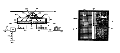
Figure 3 is a schematic illustration of a preterred embodiment of a device 301 used
in reading and authenticating a diffraction surface 302. Also illustrated in figure 3 is some
15 of the electronics associated with operating the device 301. Figure 3(a) illustrates the
device 301 in side cutaway view~ while tig~lre 3(h) ilhlstrates a front view of the device
301, omitting some of the components.
The diffraction surtace 302 is positioned by some means relative to the device 301.
The device 301 has an o~lter package 303. The device 301 also has a front window 304
20 made up of 3 regions 304a, 304b and 304c, each of said regions performing a different
function in this preferred embodiment. The window 304 may be made from a single piece
of material or may be made up of several different pieces.
It should be noted that for clarity figure 3(b) illustrates a front view of part of the
device 301 only. Specifically, figure 3(b) does not include the window 301 and also does
25 not include the electronics associated with operation of the device 301 as shown in figure
3(a)-
The device 301 includes a laser diode light source 305 which produces a beam oflight 306. The light beam 306 is usually an asymmetrically divergent light beam. The
section 304b of the window 304 is an optical lens arrangement designed to produce from
30 the light beam 306 a collimated (i.e. parallel) reading light beam 307. The section 304b of
the window 304 may be a single component lens or may consist of a number of lenscomponents.
The reading light beam 307 is directed to the diffraction surface 302. In this
preferred embodiment the diffraction surtace 302 produces from the reading light beam
35 307 a conjugate pair of diffracted light beams 308a and 308b. Other light beams may also
be produced from the reading light beam 307 by the surface 302, but will not be
considered in the present description. The diffracted beams 308a and 308b will generally
be divergent, although some diffraction surfaces may be designed to produce convergent
beams 308a and 308b.
~_ WO 94/06097 21 4 3 9 5 2 PCr/AU93/00455
As described herein, the diffracted beams produced by the diffraction surface 30'
have characteristic and machine readable Intensity Patterns which patterns result from the
diffractive structure incorporated into the diffraction surface 302.
The diffracted beam 308a passes throllgh the section 304a of the window 304 and
5 onto an optical sensor 309. The section 304a of the window 304 should ideally cause no
distortion of the beam 308a. In figure I the section 304a of the window 304 is thin and
planar and therefore does not significantly distort the beam 308a.
The optical sensor 309 is an array of separate optical detection regions 310 enabling
a measurement of the optical Intensity Pattern 311 of the diffracted beam 308a at the
IO optical sensor 309 in order to authenticate the diffraction surface 302.
- The optical detector array 309 may be configured in one of a number of different
ways. In figure 3, the optical delector array 309 is made up of a number of optical
detection regions 310 each of whicll measures incident optical intensity. The optical
detector array therefore enables a measuremellt of the Intensity Pattern of the diffracted
15 beam 308a by measuring the optical intensity of the diffracted beam 308a at a number or
different points corresponding to the optical detectors 310. The optical detector array 309
provides electronic signals 312 at the OUtpllt 313 whicll electronic signals 312 are
representative of the OUtplltS of the optical detectors 310 making up the optical detector
array 309, and therefore representative of the optical Intensity Pattern of the beam 308a at
20 the optical detector array 309.
The electronic signals 312 representing the Intensity Pattern of the beam 308a are
compared with a specified set of values 314 in an electronic device 315. The set of values
314 is stored in an electronic memory 316 and represents an authentic or "template"
optical Intensity Pattern . Tlle electronic device 315 therefore compares the measured
25 optical Intensity Pattern, as represented by the signals 312, with a "template" optical
Intensity Pattern, as represented by the signals 314, in order to determine whether or not
the measured optical Intensity Pattern matches the template to within reasonable error.
The comparison device 315 produces an OUtp~lt signal 317 at the output 318 to
indicate whether or not the measured and template optical Intensity Patterns match, to
30 within reasonable error.
The measured optical Intensity Pattern results from the diffractive structure
incorporated into the diffraction surface 302. The template Intensity Pattern corresponds
to an authentic diffraction surtace. Hence matching of the signals 312 representing the
measured optical Intensity Pattern and the signals 311 representing the template optical
35 Intensity Pattern is an indication that the diffraction surface 302 is authentic, whereas non-
matching is an indication that the surface 302 is not authentic.
Different diffraction surfaces, with different diffracted beam Intensity Patterns, can
be produced and used in different applications. Each of the different diffraction surfaces
has a corresponding "template" optical Intensity Pattern 314 to be stored in the memor
2143952 ~ .
WO 94/06097 PCr/AU93/00455
device 316. Therefore each diffraction surface reader device will store template optical
Intensity Pattern values 314 corresponding to the type or types of diffraction surface for
which the reader is intended. It should be appreciated that a diffraction reader 301 may
store more than one "template" optical lntensity Pattern, thereby enabling the reader to be
5 used with any of the corresponding types of the diffraction surface.
The diffracted beam 308b, which in this preferred embodiment is conjugate to thediffracted beam 308a, passes through the section 304c of the window 304 and onto an
optical sensor 319 which differs in design and function from the optical sensor 309. The
section 304c of the window 304 is an optical lens or combination of optical lenses which
10 acts to image the area of the diffraction surface 302 illuminated by the reading beam 307
onto the surface of the optical sensor 319~ thereby producing an image 320. In some
designs the image 320 formed a~ the optical sensor 319 may be magnified or minified
relative to the illuminated area at the diffraction surface 302. Hence the image 320
produced at the optical sensor 319 will not be the diffracted beam Intensity Pattern, as is
15 the case with the diffracted beam 308a and optical sensor 309, but will instead be an
image of any pattern recorded in the diffraction surface 302.
The purpose of the optical sensor 319 is to read any information recorded as a
pattern on or in the diffraction surface 302. The optical sensor 319 includes one or more
optical detection regions 321 each confioured according to the type of pattern anticipated
20 at the optical sensor 319. More tllan one optical detection region 321 may be included on
the optical sensor 319 since the position of the image 320 on the optical sensor 319 will
depend on the relative orientation of the device 301 and the diffraction surface 302, and
hence the inclusion of a number of optical detection regions 321 will help ensure that the
image 320 is detected regardless of its position on the optical sensor 319.
25 In one preferred embodiment the diffraction surface 302 may have a bar code data
sequence recorded on it in some manner, in which case each optical detection region 321
will preferably be a single optical detector whicll may have an active detection area
shaped either as a spot or as a narrow slit (as illustrated in figure 3) parallel to the
anticipated direction of the bars in the bar code image 320 formed at the optical sensor
30 319, the diameter of said spot or the width ot said slit geometry governing the resolution
of the bar code reading operation at the optical sensor 319.
In another preferred embodiment the diffraction surface 302 may have a two
dimensional array of pixels recorded on or in it hl some manner so as to represent
information in a machine readable form, in which case each optical detection region 321
35 may preferably be a linear or two dimensional array of optical detector elements with the
long axis of said array positioned parallel to the anticipated direction of one of the axes in
the two dimensional array image 320 produced at the optical sensor 319.
Regardless of the type of pattern recorded in the diffraction surface 302, relative
.= movement of the reading beam 307 and diffraction surface 302 will cause a change in the
~ WO 94/06097 21 4 3 9 5 ~ t PCI/AU93/00455
g ,
region of the diffraction surface 302 illuminated by tlle reading beam 307 and hence will
result in movement of the pattern in the image 320 on the surface of the optical sensor
319. By the process of relative movement of the reading beam 307 and diffraction surface
302 information recorded as a pattern in the diffraction surface 302 can be detected by
5 one or more of the optical detection regions 321 on the surface 319.
The optical detection regions 3~1 produce electronic signals 322 at the output 323
which electronic signals 322 are representative of the optical signals at the optical
detection regions 321. For example, in one preferred embodiment the signals 322 may be
made up of the outputs of the optical detectors 321 interleaved together. The electronic
10 signals 322 are fed to an electronic device 324 which processes the signals 322 to produce
an output signal 325 at the output 326 which signal 3~5 is representative of the data read
from the diffraction s~lrface 302. In one preterred embodiment the electronic device 32~
may select and process from ~he oUtp~lts of the optical detection regions 321 that output
which has the greatest signal to noise ratio.
The position of the optical Intensity Pattem 311 of the diffracted beam 308a on the
optical detector array 309 will vary depending on the relative orientation of the reading
device 301 and diffraction surtace 302. However, it is intended tl1at authentication of the
diffraction surface 302 via comparison of the Intensity Pattern 311 with a "template"
Intensity Pattern stored in the memory device 316 be possible regardless of the position of
20 the Intensity Pattern 311 on the optical detector array 309, provided that the required
diffracted beam Intensity Patterns do fall on the optical detector array 309.
In order to improve the efficiency of the electronic comparison device 315 it may be
advantageous for the device 315 to be able to determine the timing of the portion of the
signal 312 representing the Intensity Pattern 311. This can be achieved in one of a number
25 of ways, for example in one preferred embodiment this could be achieved by deliberately
including in the optical Intensity Pattern 311 an optical feature which acts as a "start"
signal for the electronic comparison de~ice 315.
It should be appreci~ted that nulllerous variations are possible on the techniques and
devices described herein. Some of the possible variations are described below.
In figure 3 the optical detection elements 310 making up the optical detector array
309 are arranged in a Cartesian layout i.e. square or rectangular. However, it should be
appreciated that the optical detection elements 310 co~lld instead be arranged in a different
manner. For example the optical detection elements 310 could be arranged in a
radial/circumferential layout.
In some applications it will be necessary to authenticate a diffraction surface without
reading any information recorded in the surtace. In sllch applications a simplified version
of the device shown in figure 3 could be used, where said simplified device would not
include the optical sensor 319 or the electronic device 3~4, and where the remaining
components may in some embodiments be re-arranged while still performing similar
WO 94/06097 21~ 3 9 5 2 PCr/AU93/00455
functions.
The optical detection regions 321 may be overlaid with masks in order to achievethe appro~,.iate active optical detection area and spatial filtering of the incident optical
beam.
5 Measurement and comparison of the optical Intensity Pattern 311 of the diffracted
beam 308a may not be required at all points on the diffraction surface 302 in order to
authenticate the surface 302. Instead, confirmation of the Intensity Pattern 311 of the
diffracted beam 308a may only be required at a predetermined number (or more) of points
or at a number of predetermined locations on the diffraction surface 302 in order to
10 authenticate the diffraction surface 302.
It may be an advantage not to opeMte the device 301 continuously during
authentication and reading of a diffraction surface. For example, it may be an advantage
not to measure continuollsly the optical Intensity Pattern 311 of the diffracted beam 308a,
but instead to take "snapshots" of the Intensity Pattern 311. This could be done using one
15 of a number of techniques. In one preferred embodiment the laser diode 305 may be
pulsed between lower and- upper power OUtpllt le~els at an appropriate repetition rate and
with an appropriate duty cycle to obtain the required "snapshots" of the Intensity Pattern
311 from the optical detector array 309. Pulsing the laser diode 305 has the advantage of
reducing the thermal energy generated by the laser diode and hence reducing the heat
20 dissipation requirement for the reader device. Pulsing of the laser diode, if carried out,
would need to be done under conditions whicll do no~ impede reading by the optical
sensor 319 of information recorded in the ditfraction surface 302. In another preferred
embodiment, said "snapshots" could be obtained by electronically "shuttering" the optical
detector array 309.
25 The device 301 as illustrated in figure 3 uses a single light source to generate a
single optical reading beam 307 directed to the diffraction surface 302. It should be
appreciated that multiple optical reading beams, at the same or different wavelengths,
generated by one or more optical sources, could be used in the reading device 301 instead
of the single optical reading beam 307 illustrated in figure 3. In this case each optical
30 reading beam produces a pair of diffMcted beams 308a and 308b as illustrated in figure 3.
Said multiple optical reading beams could be directed all to the same point or to different
points on the diffraction surface 302 and may be incident on the diffraction surface at the
same or different angles.
In one preferred embodiment a nurnber of optical reading beams, all of the-same
35 wavelength, generated by one or more optical sources, may be incident on the same
region of the diffraction surface 302 from different directions. An advantage of using
multiple optical reading beams in this manner is that multiple diffracted beams will be
produced in different directions, one ot type 308a and one of type 308b for each incident
optical reading beam, thereby increasing the probability that for a given relative
~_ WO 94/0COg7 2 1 4 3 9 5 2 ~ ` . t , PCI /AU93/00455
orientation of the device 301 and diffraction surface 30 at least one diffracted beam of
the type 308a and at least one diffMcted beam of the type 308b will fall on the optical
sensors 309 and 319 respectively thereby enabling the reader device to operate over a
greater range of relative orientations of the device 301 and diffraction surface 302.
-5 The diffraction surface 302 illustrated in figure 3 produces only a single pair of
conjugate diffracted beams - namely the beams 308a and 308b. It should be appreciated
that other diffraction surfaces may be designed to produce more than these two diffracted
beams and consequently that more than one diffracted beam Intensity Pattern 311 may
occur at the optical detector array 309. Authentication of such a diffraction surface may
lO require confirmation (via the comparison device 31S as described herein) of only one of
said diffracted beam Intensity Patterns at the optical detector array 309, or may instead
require confirmation of a number of said diffracted beam Intensity Patterns at the optical
detector array 309. The memory device 316 will be required to store "template" Intensity
Patterns for those optical Intensity Patterns which require confirmation, uhich may mean
15 that the memory device 316 must be capable ot storing more than one "template" Intensity
Pattern.
The above descriptions are in terms of reflective sllrfaces. It should be appreciated
however that the same principles can be applied to transmissive sllrfaces in which case the
device illustMted in Figure 3 will have the light source and optical sensors on opposite
20 sides of the diffraction surface.