Note: Descriptions are shown in the official language in which they were submitted.
21 55269
-1-
LIQUID CRYSTAL DEVICE HAVING UNIAXIAL AND NON-UNIAXIAL
ALIGNr~IENT CHARACTERISTIC SUBSTRATES
FIELD (~F THE INVENTION AND RELATED ART
The present invention relates to a liquid
crystal device, i.e., an optical modulation device
using a liquid crystal as an optical modulation
substance, for use in a terminal display for
computers, wordprocessors and type writers, television
receivers, a view finder for video cameras, a light
valve for projectors, a light valve for liquid crystal
printers, etc., particularly a liquid crystal device
using a chiral smectic-phase liquid crystal driven by
utilizing a spontaneous polarization such as a
ferroelectric liquid crystal and an anti-ferroelectric
liquid crystal and capable of exhibiting good display
characteristics.
There has been known a CRT as the hitherto
most widely used display device, which has been widely
used for outputting TV and VTR motion pictures or as a
monitor device for personal computers. The CRT
however has inferior stable picture characteristics,
such as a low observability due to flicker or
occurrence of scanning fringes caused by insufficient
resolution, and deterioration of the fluorescent tube
because of burning. Recently, it has been also found
that electromagnetic wave generated from a CRT exerts
ill effects to human bodies and is thus liable to
21552fi~
-2-
impair the health of a VDT operator. Further, the CRT
structurally requires a large space behind it and
hinders the space economization. As a solution of
such CRT, there has been known liquid crystal display
devices, inclusive of, e.g., a type using twisted
nematic (TN) liquid crystal as proposed by M. Schadt
and W. Helfrich, Applied Physics Letters, Vol. 18, No.
4 (February 15, 1971), p.p. 127 - 128.
As a type of liquid crystal device using a TN
liquid crystal, a simple matrix-type device has been
known as economically inexpensive. This type of
device however involves a difficulty of causing
crosstalk when driven in a multiplex manner with a
matrix electrode structure of a high pixel density, so
that the number of pixels has been restricted thereby.
In recent years, in contrast with such a
simple matrix-type device, there has been developed an
active matrix-type liquid crystal device equipped with
a TFT (thin film transistor) at each pixel. This
type of device has solved the problem of crosstalk or
response speed but is accompanied with a problem that
the commercial production of a liquid crystal device
free from a defective pixel becomes increasingly
difficult as the device area size is larger and, even
if it is possible, a tremendous production cost can
accrue.
As a type of liquid crystal device having
zl~5z~~
-3-
solved such problems of the conventional type of
liquid crystal devices, there has been proposed a
liquid crystal device of the type which controls
transmission of light by utilizing the refractive
index anisotropy of ferroelectric liquid crystal
molecules in combination with a polarizing device by
Clark and Lagerwall (U. S. Patent No. 4,367,924, etc.).
The ferroelectric liquid crystal has generally chiral
smectic C phase (SmC*) or H phase (SmH*) in a specific
temperature range and, under this state, shows a
property of taking either one of a first optically
stable state and a second optically stable state
responding to an electric field applied thereto and
maintaining the resultant state in the absence of an
electric field, namely a bistable memory
characteristic and also has a quick response speed
because it causes an inversion switching based on its
spontaneous polarization. Further, the ferroelectric
liquid crystal also has an excellent viewing angle
characteristic and is therefore considered as suitable
for providing high-speed, high resolution and large
area display devices and light valves.
There is also known an anti-ferroelectric
liquid crystal as an optical modulation material
capable of providing display device similarly based on
utilization of the refractive index anisotropy and
spontaneous polarization of liquid crystal molecules.
-4-
The anti-ferroelectric liquid crystal has generally a
chiral smectic CA phase (SmCA*) and, in this phase,
has an average optically stable molecular axis aligned
with a smectic layer normal direction in the absence
of an electric field but has an average optically
stable molecular axis tilted from the layer normal
direction under application of an electric field.
Further, the anti-ferroelectric liquid crystal also
causes switching based on the coupling between the
spontaneous polarization and an applied electric
field, so that it shows a very quick response speed
and is expected to provide high-speed display devices
and light valves.
A problem of a display panel composed by a
liquid crystal device using a ferroelectric liquid
crystal or anti-ferroelectric liquid crystal is to
provide a defect-free alignment state for maintaining
a good contrast. In order to form a good liquid
crystal alignment state, a device (structure)
including a pair of substrates having asymmetrical
alignment control layer, i.e., alignment control
layers of different materials or different alignment
characteristics, has been proposed, e.g., by Japanese
Laid-Open Patent Application (JP-A) 61-20930. For
example, one of the substrates is provided with a
uniaxial alignment characteristic and the other is
provided with a non-uniaxial alignment characteristic,
21552 69
-5-
whereby the liquid crystal can be aligned at a high
controlling order from the side of the substrate
provided with the uniaxial alignment characteristic to
facilitate the formation of a good liquid crystal
alignment state.
On the other hand, in the case where a pair
of liquid crystal boundaries are provided with
different alignment characteristics, the alignment
state may be apparently good but the switching
characteristics are liable to be asymmetrical and the
good bistability of a ferroelectric liquid crystal can
be impaired to result in inferior switching memory
characteristic.
In order to solve the problem, JP-A 62-235928
and JP-A 63-228130 have proposed to control the
polarities of the surface of a pair of substrates, but
a further improvement may be necessary in order to
stabilize the overall behavior of the liquid crystal.
Particularly, it may be required to provide a liquid
crystal device which has a simple structure and can be
produced at a low cost.
Particularly, the symmetricity of switching
characteristic is also important to provide a broader
drive margin. The symmetrical switching
characteristic has to be retained even on continuation
of drive for a long period.
Further, in a display panel comprising a
21552fi9
-6-
liquid crystal device using a ferroelectric liquid
crystal or an anti-ferroelectric liquid crystal, a
reverse electric field induced by a spontaneous
polarization of the liquid crystal per se has been
another important problem to be considered,
particularly in order to effect a halftone display.
More specifically, a desired halftone can be made
instable due to an electric field caused by internal
ions localized corresponding to the spontaneous
polarization, and a hysteresis in optical response can
occur in response to an externally applied electric
field. More specifically, corresponding to the
direction of spontaneous polarization of liquid
crystal molecules in the "black" state or the "white"
state, respectively, ions are localized in directions
so as to stabilize the respective states and, due to a
difference in polarity of localization, the
application of an identical voltage Vw after a short
period of resetting (into "black") can exert actually
different voltages applied to the liquid crystal
depending on whether the previous state is "white" or
"black" state.
As an extremely inadequate phenomenon caused
by the above-mentioned reverse electric field, a
switching failure may be caused such that, e.g., when
a pixel is reset into a black state and then intended
to be written into a white state, the written "white"
21552 69
state is not latched by application of a prescribed
voltage level but can be returned into a "black"
state. This is a fatal defect even in a display panel
not requiring a halftone level at each pixel.
As a countermeasure to the above-mentioned
reverse electric field, JP-A 63-121020, for example,
has proposed to provide a ferroelectric liquid crystal
device with an alignment control film of a low
impedance in order to cope with a switching failure
due to the reverse electric field. Further, JP-A 2-
153321 has disclosed low-impedance alignment control
film comprising various species of organic conductive
films. Further, JP-A 64-49023 has proposed to form a
thin alignment control film on a passivation film for
short circuit prevention which has been made a low
impedance. However, it is a present state that these
proposals have not provided a sufficient solution.
In this way, the electrooptical
characteristics of the liquid crystal device using a
chiral smectic liquid crystal has left rooms for
further improvement with respect to control of an
alignment state, a reverse electric field caused by a
spontaneous polarization, and a change in threshold
characteristic and an optical response instability
depending on a preceding standing state.
-g_
21 552 fig
SUMMARY OF THE INVENTION
In view of the above-mentioned circumstances,
an object of the present invention is to provide an
asymmetrically aligning treated liquid crystal device
which may be produced at a low cost and is provided
with good switching characteristic and alignment
characteristic resistant to long hours of drive.
A more specific object of the present
invention is to provide a liquid crystal device with
stable optical response characteristic inclusive of a
good liquid crystal alignment state, a reduced
asymmetry of switching and an ensured stability of two
states of a liquid crystal (particularly, a
ferroelectric liquid crystal or an anti-ferroelectric
15~ liquid crystal).
A further object of the present invention is
to provide a liquid crystal device allowing excellent
halftone display, particularly by preventing an
adverse influence of a reverse electric field caused
bY a spontaneous polarization of a liquid crystal per
se in case of a halftone display using a ferroelectric
liquid crystal or anti-ferroelectric liquid crystal.
According to the present invention, there is
provided a liquid crystal device, comprising a pair of
oPPositely disposed substrates including a first
substrate having a uniaxial alignment characteristic
and a second substrate having a non-uniaxial alignment
21 ~~z s9
_g_
characteristic and a liquid crystal disposed between
the first and second substrates, wherein
said first and second substrates have surface
potentials providing a difference therebetween of less
than 50 mV in terms of an absolute value at their
liquid crystal-contacting surfaces.
According to another aspect of the present
invention, there is provided a liquid crystal device,
comprising a pair of oppositely disposed substrates
including a first substrate having a uniaxial
alignment characteristic and a second substrate having
a non-uniaxial alignment characteristic and a liquid
crystal disposed between the first and second
substrates, wherein
at least the second substrate having a non-
uniaxial alignment characteristic is provided with a
film having a volume resistivity of 104 - 108 ohm. cm.
According to a further aspect of the present
invention, there is provided a liquid crystal device,
comprising a pair of oppositely disposed substrates
including a first substrate having a uniaxial
alignment characteristic and a second substrate having
a non-uniaxial alignment characteristic and a liquid
crystal disposed between the first and second
substrates, wherein
said first and second substrates have surface
potentials of an identical polarity at their liquid
21552 69
-10-
crystal-contacting surfaces.
According to a still further aspect of the
present invention, there is provided a liquid crystal
device, comprising a pair of oppositely disposed
substrates including a first substrate having a
uniaxial alignment characteristic and a second
substrate having a non-uniaxial alignment
characteristic and a liquid crystal disposed between
the first and second substrates, wherein
said second substrate having a non-uniaxial
alignment characteristic is provided with a film
having a volume resistivity in the range of 104 - 108
ohm. cm.
These and other objects, features and
advantages of the present invention will become more
apparent upon a consideration of the following
description of the preferred embodiments of the
present invention taken in conjunction with the
accompanying drawings.
BRIEF DESCRIPTION OF THE DRAWINGS
Figure 1 is a sectional view of an embodiment
of the liquid crystal device according to the
invention.
Figure 2 is a schematic illustration of a
surface potential measurement system adopted in
defining the invention.
-11-
21 55269
Figure 3 is a schematic illustration for
explaining a concept of internal potential in a liquid
crystal deice of the invention.
Figures 4A - 4D are respectively an internal
potential state in a liquid crystal device of the
invention.
Figure 5 is a schematic sectional view for
illustrating a liquid crystal molecular alicxnmerit
state in an embodiment of the liquid crystal device
according to the invention.
Figures 6A and 6B are schematic partial
sectional illustrations of explaining a function of a
liquid crystal device according to the invention.
Figure 7 is an equivalent circuit diagram of
a liquid crystal device according to the invention.
Figure 8 is an equivalent circuit diagram of
a conventional liquid crystal device.
Figure 9 is an illustration of a system for
measuring a volume resistivity of a coating. film or a
Passivation film in a thickness direction in a liquid
crystal device according to the invention.
Figures l0A and 108 are respectively a
schematic plan view of an electrode pattern and a
sectional view of a system for measuring a volume
resistivity of a coating film in a sheet extension
direction in a liquid crystal device according to the
invention.
-12- 21 552 69
Figures 11 and 12 are graphs showing a
relationship between a measured surface potential and
a switching threshold in liquid crystal devices
prepared in Experimental Examples 1 and 2,
respectively.
Figure 13 is a sectional view of a liquid
crystal device together with indication of a surface
potential measurement system used in an Experimental
Example appearing hereinafter.
Figure 14 is a graph showing a hysteresis and
switching asymmetricity in V (voltage) - T
(transmittance) curve of a liquid crystal device in an
Experimental Example appearing hereinafter.
DESCRIPTION OF THE PREFERRED EMBODIMENTS
According to the present invention, in a
liquid crystal device using a liquid crystal showing a
chiral smectic phase, particularly a ferroelectric
liquid crystal or an anti-ferroelectric liquid
crystal, and provided with an asymmetry, i.e.,
including a combination of a first substrate having a
uniaxial alignment characteristic and a second
substrate having a non-uniaxial alignment
characteristic, the direction of spontanedus
polarization of liquid crystal molecules at the
respective boundary surfaces (so-called "outward
characteristic~~or "inward characteristic") may be
-13- 21 552 69
adjusted to ensure a symmetry of switching
characteristic and stably equalize the switching
bistable potentials.
As a result, in the above-descried device, it
becomes possible to suppress the occurrence of
alignment defects or defects caused at Structurally
foreign parts, such as spacers or stepwise difference,
e.g., those between pixels, while realizing good
memory characteristic and margin characteristic.
Herein, the term "uniaxial alignment
characteristic" means a uniaxial homogenous alignment
characteristic of a substrate, i.e., the property of a
substrate or an alignment film formed thereon of
aligning liquid crystal molecules in contact therewith
in one direction parallel to its planar extension
while having the possibility of some pretilt of the
liquid crystal molecules with respect to the substrate
surface. On the other hand, the non-uniaxial
alignment characteristic is ai property of a
substrate, i.e., the property of a substrate or a film
formed thereon of providing liquid crystal molecules
in contact therewith with an alignment state other
than the uniaxial homogeneous alignment state,
inclusive of a homeotropic alignment state and a
random alignment state.
In the liquid crystal device according to the
present invention, it is preferred to first establish
9
-14-
an identical polarity of surface potentials on both
substrates and then set the surface potential values
on both substrates to satisfy the above-mentioned
prescribed relationship, i.e., a surface potential
difference of at most 100 mV, more preferably at most
50 mV, in terms of an absolute value (i.e., within the
range of ~100 mV, preferably ~50 mV). The surface
potential difference may preferably be at most 30 mV.
It is further preferred that the surface potentials on
both substrates are substantially identical to each
other, so as to stably retain a better symmetrical
switching characteristic.
More specifically, in the liquid crystal
device according to the present invention, one
substrate is provided with a layer (alignment control
layer) having a uniaxial alignment characteristic, as
defined above, inherently or as a result of an
appropriate treatment applied thereto, and the other
substrate is provided with a non-uniaxial alignment
layer (i.e., a layer not having a uniaxial alignment
characteristic). A liquid crystal is disposed between
these substrates. Further, by optimally selecting the
materials and forming conditions of these alignment
control layer, non-uniaxial alignment layer and other
members on the substrates, such as transparent
electrodes, a short circuit-prevention film and other
functional films, the surface potentials on both
21 55289
-15- -
substrates are controlled as described above.
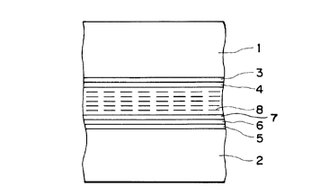
Figure 1 is a schematic sectional view of an
embodiment of the liquid crystal device according to
the present invention. Referring to Figure d, a
liquid crystal device (cell) includes a pair of
substrates 1 and 2, and a liquid crystal 8 disposed
between the substrates. One substrate 1 is provided
with, on its inner surface contacting the liquid
crystal, electrodes 3 and an alignment control layer 4
so as to provide a surface having a uniaxial alignment
characteristic of aligning liquid crystal molecules in
one direction substantially parallel thereto. The
other substrate 2 is provided with electrodes 5 and a
film (preferably, a coating film) 6, e.g., one
comprising a matrix of an oxide or a polymer and
ultrafine particles of an oxide or metal dispersed
therein. As desired, the film 6 may be further coated
with an additional film 7 of, e.g., a known silane
coupling agent. As a result, the substrate surface is
provided with a non-uniaxial alignment characteristic.
The film 6 may preferably have a thickness of
300 - 5000 A. Materials of the film 6 may preferably
be selected so as to adjust the polarity of the
surface potential, the resistivity~ and the surface
characteristic of the substrate on which the film 6 is
formed. For example, the film 6 may preferably be
formed as a film containing various metal or metal
21 ~~~ 69
-16-
oxide. Further, in order to obviate an adverse
influence of a reverse electric field inherent to a
chiral smectic liquid crystal having a high Ps
(spontaneous polarization), the film 6 may preferably
have a volume resistivity of 104 - 108 ohm. cm, more
preferably 104 - 10~ ohm.cm, as measured in the
direction of its layer extension as will be described
hereinafter.
The electrodes 3 and 5 may preferably
comprise a transparent conductor, such as tin oxide,
indium oxide or ITO (indium tin oxide). However, when
light transmissivity is not required, the electrode 3
or 5 can comprise a metal such as Cr, A1 or Ta.
The alignment control layer 4 may suitably
comprise a uniaxially aligning-treated film of an
organic material, such as polyimide, nylon or
polyvinyl alcohol, or an electroconductive polymer,
such as polyanyline or polypyrrole. Particularly, it
is preferred to use a film of a known material as
described above subjected to a uniaxial aligning
treatment by rubbing. Alternatively, the alignment
control layer 4 may also comprise a film of an
inorganic material such as a silicon oxide film formed
by oblique vapor deposition. In this case, the
uniaxial aligning characteristic can be provided by
appropriately controlling the oblique vapor deposition
conditions even without effecting the above-mentioned
2155269
-17-
rubbing operation.
On the other hand, the optionally provided
film 7 having a non-uniaxial alignment characteristic
can comprise a vapor-deposited film of a vaporizable
silane coupling agent or vapor-deposited or coating
film of amorphous inorganic material in addition to
the above-described coating film of a silane coupling
agent. The film 7 may preferably be formed in a
thickness of at most 50
The film 7 may be provided, if necessary, as
described above, or the film 6 per se can provide a
surface having a non-uniaxial alignment
characteristic. Further, instead of uniformly coating
the film 6, the optional film 7 may preferably coat
the film 7 so as to frequently expose the film 6 at a
large number of points.
The liquid crystal layer 8 may preferably
comprise a chiral smectic liquid crystal (i.e., a
liquid crystal assuming a chiral smectic phase),
particularly one showing a spontaneous polarization
inclusive of a ferroelectric liquid crystal and an
anti-ferroelectric liquid crystal so as to enjoy
advantageous effects accompanying the device
structural characteristic of the present invention.
It is, however, also possible to use another liquid
crystal material, such as a nematic liquid crystal.
In the case of using a chiral smectic liquid
2155269
-18-
crystal, particularly a ferroelectric liquid crystal
or an anti-ferroelectric liquid crystal, in the device
structure according to the present invention, it is
particularly effective to use a liquid crystal
material showing a phase transition series on
temperature decrease of Iso. (isotropic phase) --~ SmA
(smectic A phase) -~ SmC* (chiral smectic phase)
Cryst. (crystal phase) in view of its alignment
characteristic.
In order to provide a liquid crystal device
exhibiting an improved display brightness, it is
preferred to use a chiral smectic liquid crystal
material providing a bookshelf structure in which
smectic liquid crystal molecular layers in SmC* phase
stand perpendicularly or with a slight inclination
from a normal to the substrates. Examples of such a
chiral smectic liquid crystal material may include a
composition containing a fluorine-containing
mesomorphic compound having a central core to which a
fluorocarbon terminal portion and a hydrocarbon
terminal portion are connected, and showing a smectic
phase or a latent smectic phase. Examples of such
fluorine-containing compounds may include those
disclosed in U.S. Patents Nos. 5,082,587 and
5,262,082, PCT International Publication WO 93/22936,
etc.
More specifically, it is preferred to use a
21552 sg
-19-
liquid crystal material containing such a fluorine-
containing compound appropriately selected and showing
the above-mentioned phase transition series of Iso. --y
SmC --~ SmC* -~ Cryst., i.e., not showing Ch.
(cholesteric phase), on temperature decrease.
The above-mentioned device according to the
present invention basically has an asymmetric
structure wherein only one substrate surface has a
uniaxial alignment characteristic (has been uniaxially
aligning-treated), and wherein a liquid crystal
(particularly a ferroelectric liquid crystal or an
anti-ferroelectric liquid crystal) is aligned
particularly in its SmA temperature region as a
uniaxial molecular growth propagating from the surface
of the substrate having a uniaxial alignment
characteristic, thereby providing a good alignment
state in the SmC* phase.
Particularly, in the case of using the above-
mentioned chiral smectic liquid crystal showing no
cholesteric phase, the asymmetrical device structure
according to the invention is preferred so as to
effect a good alignment control at the time of Iso ---
SmA phase transition on temperature decrease, thereby
realizing a uniform alignment state.
Hereinbelow, some detailed description will
be made regarding the surface potential and its
measurement method and the function attributable to
2155269
-20-
the surface potential characteristic defined and
utilized in the present invention.
The surface potential defined herein is a
composite potential induced at a film surface caused
by a potential due to a polarity of a surface-forming
film per se, an electrical double layer potential due
to a carrier migration with a lower layer film, a
potential due to ionic molecules contained in the
film, etc., and may be measured according to the
following method.
Regarding the measurement of such a surface
potential as descried above, reports have been made on
polyimide film as a generally known liquid crystal-
alignment film by Ito and Iwamoto (Tokyo Institute of
Technology), Journal of Electrostatics, 17, 5, pp. 352
- 358 (1993); Journal of Electrostatics, 33, pp. 147 -
158 (1994), etc. Based on phenomena that the surface
potential of a polyimide film is remarkably varied
depending on the kinds of lower metal films, the
direction and magnitude of the variation are related
with the work functions of the metal films, and the
surface potential varies depending on the polyimide
film thickness and is saturated around 5 nm which may
be the tunneling limit of carriers, Ito et al have
concluded that the surface potential is principally
caused by an electrical double layer due to carrier
movement between the film and the electrode.
-21- 2155269
As apparatus for surface potential
measurement, there have been known a vibration
capacitance type and a sector-type according to the
capacitance type, and a pyroelectricity type according
to the resistance type. The surface potential values
referred to herein are based on values measured~by
using a vibration capacitance-type surface potential
meter ("Model 320B", available from Trek Corp.). More
specifically, various liquid crystal-contacting films
of a uniaxial alignment characteristic were
respectively formed on a lower layer structure
actually adopted in an actual cell structure including
a transparent electrode film and a lower layer of a
short circuit prevention film, etc., thereon and the
surface potential of the respective films were
measured. As a result, the measured values of surface
potential remarkably varied in the range of roughly
+500 to -500 mV depending on the materials of the film
per_se and the lower lay-er.
Moreover, according to our experiments, the
measured values of surface potential remarkably depending on
polar molecules absorbed on the surface.
Particularly, a film material having a high
hygroscopicity can provide remarkably different
measured values between a vacuum environment and the
atmospheric environment. Regarding a liquid crystal-
contacting surface in a liquid crystal device, the
2155269
-22-
liquid crystal injection into the liquid crystal
device is frequently performed under heating in a
vacuum environment. Accordingly, in some cases, after
water molecules adsorbed on a surface is liberated by
evaporation and then some molecules in the liquid
crystal material can be adsorbed and fixed on the
surface to develop a new surface potential.
Accordingly, the measurement of surface potential
should preferably be performed in an environment
equivalent to a liquid crystal-injection environment
for a particular device concerned.
Figure 2 is a schematic illustration of an
apparatus suitably used for measurement of surface
potential adopted in the present invention (i.e.,
based on the above-mentioned vibration capacitance-
type surface potential meter ("Model 3208", Trek
Corp.). Referring to Figure 2, the measurement is
performed in a vacuum chamber 35 connected to a vacuum
exhaust system 32 and a gas supply system 33 for
supplying dry nitrogen, etc. A sample film 21 for
surface potential measurement is formed on a lower
structure, which is basically identical to that
contained in a device actually contemplated, including
an identical substrate 23 and an identical electrode
22 (and an identical lower layer, if any) and under
identical conditions as in the device, the substrate
23 carrying the sample 21 is disposed on a heating bed
21 ~ ~ ~ ~:
-23-
30 of which the temperature is controlled by a
temperature controller 31 placed outside the vacuum
chamber 35.
A surface potential measurement probe 24 is
composed of a sensor electrode 25, a preamplifier and
a vibrating element 26 for vibrating the electrode 22
to modulate the capacitance between the sample film 21
and the electrode 23, and is connected to a surface
potential measurement and control apparatus 27
disposed outside the vacuum chamber 35.
Specific surface potential measurement
conditions to be adopted may correspond to standard
liquid crystal injection conditions. For example,
measurement may be performed after heating a sample at
a temperature of 80 - 100 °C for 15 min. to 2 hours
under a reduced pressure of 10-1 to 10 3 torr. and
cooling to room temperature. First, the gap between
the surface of the electrode 22 and the sensor
electrode 25 is held at an appropriate value around
0.5 - 5 mm by a biaxial displacement apparatus 34 to
measure a surface potential at an exposed part of the
electrode 22 adjacent to the sample film 21. Then,
the sensor electrode 25 is moved to above the sample
film 21 by the biaxial displacement apparatus 34 to
measure a surface potential thereat. The surface
potential of the sample film is determined by
subtracting the measured surface potential at the
~l~5zs9
-24-
exposed electrode part as the reference potential from
the directly measured surface potential at the sample
surf ace .
In some cases, a surface potential in the
state where liquid crystal molecules are adsorbed on
the surface through the liquid crystal injection step
is considered to govern an internal potential applied
between the substrates. Accordingly, in actual cases,
it is preferred to perform repetitive experiments
under comparative conditions and adopt a measured
value obtained under a condition giving a better
correlation. For this purpose, a liquid crystal 28
may be placed in a vessel 29 for heating evaporation
disposed on a heating table 30 so as to allow the
evaporation of the liquid crystal 28 to form a liquid
crystal vapor-containing atmosphere and cause the
liquid crystal to be adsorbed by the surface of the
sample film 21 according to necessity.
Now, the concept of an internal potential or
voltage caused by a difference between surface
potentials on oppositely disposed liquid crystal-
contacting boundaries of two substrates in a liquid
crystal device having an asymmetrical structure of the
present invention, will be described with reference to
Figure 3. Referring to Figure 3, substrates
(electrode plates) 41 and 42 are provided with a
uniaxial alignment control layer (layer having a
-25- 2 1 5 5 2 6 9
uniaxial alignment characteristic) 43 and a non-
uniaxial alignment control layer (layer having a non-
uniaxial alignment characteristic) 44, respectively,
of mutually different materials. These electrode
plates are disposed opposite to each other with a
prescribed gap therebetween to form a cell. then a
blank cell (i.e., a cell containing no liquid, crystal
therein) is constituted while short circuiting between
the electrode plates 41 and 42, a surface potential 45
and a surface potential 46 may be formed on'the layers
43 and 44, respectively, thereby forming an internal
voltage 47 therebetween.
In view of the above-mentioned measured
surface potential values, the internal voltage
occurring corresponding to the surface potential
difference can amount to ~1 volt at the maximum. The
presence of such an internal voltage due to a surface
potential difference is considered to be effectively
equal to the continual application of a DC offset
voltage between a pair of opposite electrodes. An
influence of the internal voltage due to a surface
potential difference on a switching threshold was
experimentally confirmed as follows. A cell of a
symmetrical structure including a pair of substrates
having thereon alignment control films of identical
materials and subjected to identical treatments (i.e.,
having a surface potential difference of 0) was
2~ 552 ss
prepared and supplied with a DC offset voltage in
superposition between the opposite electrodes to
evaluate the change in switching threshold, whereby a
change in switching threshold was confirmed to occur
at a DC offset voltage level of ~50 mV to one hundred
and several tens mV.
Then, based on surface potential values
measured with respect to various,alignment control
films, various alignment control~films were combined
lp to form liquid crystal cells of asymmetrical
structures as described above to'compare surface
potential differences and asymmetry of switching
threshold, whereby it has been. observed that the
polarity of surface potential~difference subst~ntially_
coincides with the direction of asymmetrical switching
threshold characteristic, and a significant-correlation is
observed between the absolute value of surface
potential difference and the degree of asymmetrical
switching threshold characteristic. More
specifically, in devices wherein surface potential
differences are small, particularly smaller than 50
mV, substantially no asymmetrical switching
characteristic appeared in many cases regardless of
surface potential polarities on both substrates.
Further, in the case where the surface potential
polarities are identical on both substrates and the
surface potential difference is within ~100 mV, there
2155269
-27-
was a tendency that substantially no switching
asymmetry. In these cases, the switching threshold
difference as a measure of a switching asymmetry can
be suppressed to a low level of within ~1.0 volt. On
the other hand, devices having larger surface
potential differences of ~100 mV to ~200 mV tended to
show an asymmetrical characteristic affecting the
drive margin. Further, devices having surface
potential differences exceeding ~250 mV cawed
switching failure and showed a loss of bistable
potential characteristic in many cases.
As described above, according to the present
invention, it has been experimentally confirmed that
an asymmetrical switching threshold characteristic in
an asymmetrically structured cell having asymmetrical
alignment control films is principally controlled by
surface potentials on the alignment control films and
the asymmetrical switching threshold characteristic
can_be suppressed by controlling the surface
potentials on the liquid crystal-contacting surfaces
of both substrates even in an asymmetrically
structured cell.
Several particularly preferred embodiments of
the present invention will be described with
reference to Figures 4A - 4D illustrating various
potential characteristics across various cells
(devices). Figure 4A shows a device wherein electrode
2~ 55z~~
-28-
plates 41 and 42 are provided with a uniaxial
alignment control layer 43 and a non-uniaxial
alignment control layer 44 of different materials
whereby surface potentials 45 and 46 of the same
polarity occur to provide a internal voltage 47 of
below 50 mV. Figure 4B shows a device having surface
potentials 45 and 46 of different polarities giving an
internal voltage 47 of below 50 mV. Figure 4C shows a
device obtained by disposing an additional film 48,
such as a short circuit prevention film, between the
electrode plate 41 and the alignment control layer 43
on one substrate, thereby providing the alignment
control layer 43 with a surface potential which is
different from the one in Figure 4B and provides an
internal voltage 47 of below 50 mV. Figure 4D shows a
device providing the layers 43 and 44 with surface
potentials 45 an 46, of which the absolute values are
respectively below 50 mW.
As described above, in the liquid crystal
device according to the present invention, it is
important to retain an appropriate relationship
regarding surface property between the surfaces having
a uniaxial alignment characteristic and a non-uniaxial
alignment characteristic on both substrates in order
to provide equal bistable potential characteristics
for switching of a ferroelectric liquid crystal or an
anti-ferroelectric liquid crystal after alignment.
21552
-29-
Further, in the case of a chiral smectic
liquid crystal inclusive of a ferroelectric liquid
crystal and an anti-ferroelectric liquid crystal,
particularly in the case of a ferroelectric liquid
crystal, it is also important to pay attention to the
direction of spontaneous polarization, i.e., whether
the spontaneous polarization is directed toward a
substrate (outward characteristic) or directed toward
the bulk of the liquid crystal (the center of the
liquid crystal layer) (inward characteristic), at the
time of SmA --~ SmC* transition, as a characteristic of
the liquid crystal-contacting surfaces of the
substrate having a uniaxial alignment characteristic
and the substrate having a non-uniaxial alignment
characteristic. The direction has been recognized to
have a strong correlation with the surface potential
polarity on the liquid crystal-contacting surface of
each substrate.
The surface potential polarity is considered
to be caused by a surface potential generated by
contact charging between an organic or inorganic film
and a metal and distribution of charge particles such
as ions in the film.
A substrate (electrode plate) in the liquid
crystal device according to the present invention may
be formed by laminating the above-mentioned alignment
film, coating film or vapor deposition film so as to
-30-
cover transparent electrodes of, e.g., ITO, formed on
a base plate. In this instance, the dipole of a
chiral smectic liquid crystal inclusive of a
ferroelectric liquid crystal and an anti-ferroelectric
liquid crystal and accordingly the switching
characteristic of the liquid crystal are inevitably
affected by the polarity and magnitude of surface
potential on both substrates having a uniaxial
alignment characteristic and a non-uniaxial alignment
characteristic. According to a preferred embodiment
of the present invention, the surface potential
polarities on both substrates are properly controlled,
preferably made identical to each other, to improve
the alignment state and switching characteristic of
the liquid crystal.
In the liquid crystal device according to the
present invention, in addition to controlling the
surface potential difference and the surface potential
polarities between both substrates as described above,
it is preferred to suppress the absolute value of
surface potential on each substrate to a smaller
value, particularly at most 100 mV, preferably at most
50 mV, in order to suppress the influence of a
substrate surface on dipoles of liquid crystal
molecules and prevent the transition into a monostable
characteristic with time.
As described above, in order to provide good
21552 69
-31-
alignment state and equal switching potentials in the
liquid crystal device according to the present
invention, it is important to appropriately select the
surface materials on both substrates. In this regard,
it has been recognized important to pay attention to a
surface tension factor as determined particularly by a
dispersion term of a surface energy as a latching
potential factor in addition to the polarity factor on
the liquid crystal-contacting surfaces of both
substrates.
The substrate having a non-uniaxial alignment
characteristic in the liquid crystal device of the
present invention may preferably have a dispersion
term of surface energy which is sufficiently small to
be at a level identical to the surface energy at a
temperature in the neighborhood of the SmA --~ SmC~'
transition temperature of the liquid crystal used,
providing a difference therefrom of at most 5 dyne/cm.
In other words, the dispersion term may preferably be
at most 30 dyne/cm. Alternatively, the dispersion
term may preferably be larger than the surface energy
of the substrate having a uniaxial alignment
characteristic or a value of at least 40 dyne/cm. The
above ranges are preferred because good switching
characteristic is attained thereby in many cases.
The above-mentioned ranges of the surface
energy (as represented by the dispersion term) are
2155269
-32-
preferred for the following reasons. In the above-
mentioned case of a low surface energy (of preferably
at most 30 dyne/cm), the liquid crystal shows a so-
called homeotropically wetting state against the non-
uniaxially aligning surface, whereby the liquid
crystal in the vicinity of the surface is almost fixed
and the switching potential is generally governed by
the inner side (bulk liquid crystal side). On the
other hand, in the case of a large surface energy (of
preferably at least 40 dynes/cm), the liquid crystal
in the vicinity of the surface is fixed by a so-called
homogeneously wet state, so that the switching
potential may be also governed by the inner side (bulk
liquid crystal side).
The surface properties of the substrate
having a non-uniaxial alignment characteristic can be
adjusted by appropriate selection of the surface
material and shape.
On the other hand, the substrate having a
uniaxial alignment characteristic may preferably have
a dispersion term of surface energy of at least 40
dyne/cm, more preferably at least 42 dyne/cm, so as to
provide good uniaxial homogeneous alignment
characteristic and a stable switching potential,
through appropriate selection of materials of the
alignment control film.
Next, the measurement of surface energy on
21552 fig
-33-
the respective substrates in a macroscopic surface
state will be described.
Reagents for providing a liquid droplet for
contact angle measurement may include for example, A:
a-bromonaphthalene, B: methylene iodide, C: water,
etc. After the measurement of contact angles with
liquids A, B and C, it is possible to use calculation
formulae descried, e.g., in Nippon Settyaku Kyokai-shi
(Journal of Japan Adhesive Society), Vol. 8, No. 3
(1972) page 131 -, Kitasaki et al, "Expansion of
Fowkes~ Formula and Evaluation of Surface Tension on
Polymer Solid" to calculate the surface energy while
noting the dispersion term thereof. On the other
hand, as described above, a surface energy may include
a polarization term and a hydrogen bond term in
addition to the dispersion term. These terms are
however closely related with the surface polarity of a
film, and a good correlation with the above-mentioned
characteristics may preferably be evaluated by noting
only the value of the dispersion term.
In the liquid crystal device having the
structure shown in Figure 1, the film 6 contained in
the substrate having a non-uniaxial alignment
characteristic is effective for adjusting the polarity
or surface state (surface energy), and further the
volume resistivity measured on the surface of the
substrate. The adjustment may be facilitated by
21 55289 :.:
-34-
appropriate selection of components based on their
properties.
It is possible to, use a film 6 comprising
specific materials so as to more appropriately control
the surface potential~~ Examples thereof may ,include
films, preferably costing-type films, comprising a
matrix of SiOx,. TiOx, ZrOx, another meltable inorganic
oxide.silica, and a polymer, such as siloxane polymer,
and ultrafine~particles dispersed therein of oxides,
inclusive of group II element oxides, such as ZnO, Cd0
and ZnCdOx; and group IV element oxides, such as Ge02,
Sn02, GeSnOx, Ti02, Zr02 and TiZrOx; and metals, such
as Pd so as to control the film property and the
resistivity of the film.
The above-mentioned oxide can contain
electroconductivity-controlling impurities added
thereto. Such electroconductivity-controlling
impurities may include: n-type impurities (donor:
impurities enhancing electron-conductivity) comprising
group III elements, such as B, A1, Ga and In, and p-
type impurities (acceptors: impurities enhancing hole-
conductivity) comprising group I elements, such as Cu,
Ag, Au and Li, respectively, for the group II element
oxides; and n-type impurities comprising group V
elements, such as P, As, Sb and Bi, and p-type
impurities comprising group III elements, such as B,
A1, Ga and In, respectively, for the group IV element
-35- 2 1 5 5 2 6 9
oxides. In case where the film 6 is used, it is
possible to apply an additional film 7 of, e.g., a
silane coupling agent, ~o as to effect a fine control
of the surface state, according to necessity, as
mentioned hereinbefore.
The effects of using such ultrafine particles
having a particle size of 30 - 300 ~, preferably 30 -
150 A, will be described below.
First, when a relatively thick film (having
a thickness of 300 - 5000 ~, preferably 1000 - 5000 A)
containing the ultrafine particles is formed, a
plurality of,the ultrafine particles can be stacked in
the film. As the above-mentioned ultrafine particles
generally have a high hardness, the stack structure
can exhibit a strong pressure resistance which is
effective for preventing short circuit between the
substrates liable to be caused by contamination of the
foreign matter within the liquid crystal cell. This
was_corroborated by a specific test wherein a 1400 A-
thick film of silica containing antimony-doped SnOx
dispersed therein showed a withstand voltage of 25
volts by an ordinary probe test performed by us.
The film containing the ultrafine particles
has been provided with a moderately lowered
resistivity, so that an excessive charge accumulation
can be avoided. This also contributes to an increase
in withstand voltage.
21552 69
-36-
Further, the film containing the ultrafine
particles can be formed in a relatively large
thickness. Accordingly, when a lower layer structure
includes a stepwise height difference, e.g., due to
formation of color filter segments, switching
elements, such as thin film transistors (TFT), and
metal electrodes for conductivity enhancement, the
stepwise height difference can be absorbed by the
film, to suppress an ill effect thereby against
alignment control function exerted by the opposite
substrate having a uniaxial alignment characteristic,
and suppress the occurrence of alignment defects
during the drive.
Furthermore, the film containing ultrafine
particles can increase the latitude of controlling the
surface potential through appropriate selection of the
film material and thickness, and other factors related
with the film.
The film containing ultrafine particles can
be provided with a surface having minute projections
with an appropriate hardness. As a result, even if
various processing is applied thereto on the substrate
having a non-uniaxial alignment characteristic, the
surface can be free from uniaxial alignment
characteristic, thus obviating alignment disorder to
provide improved characteristics.
The film 6 can be formed by two or more
2155269
-37-
materials in combination for the matrix and/or the
fine particles in order to more accurately adjust
various properties inclusive of the surface potential.
Particularly, the appropriate selection and
mixing in an appropriate ratio of polymer species for
constituting the film 6 may be effective in reducing
the surface potential difference between both
substrates to at most 100 mV, more preferably to below
50 mV, and providing both substrates with the same
polarity of surface potential. As a result, the
dipole (Ps)~ of a ferroelectric liquid crystal or an
anti-ferroelectric liquid crystal can better respond
to an external electric field.
Further, the film 6 on the substrate having a
non-uniaxial alignment characteristic in the liquid
crystal device according to the present invention can
be formed as a passivation film including laminated
plural layers.
The passivation film may preferably be
designed to provide a surface potential which is an
intermediate value among the surface potentials of
constitute single layers, when respectively measured
separately on an arbitrarily selected electrode with
reference to the electrode potential.
Particularly, if the laminate passivation
film on the substrate having a non-uniaxial alignment
characteristic is provided with a surface potential
-38-
which is different from that of the opposite substrate
having a uniaxial alignment characteristic by a
smaller value, preferably less than 50 mV, or more
preferably substantially identical to that of the
opposite substrate, a more stable switching
characteristic of a chiral smectic liquid crystal can
be obtained.
Further, a lower layer (i.e., a layer closer
to the base plate) in the laminated passivation film
may preferably be composed of a polycrystalline metal
oxide film or a polycrystalline semiconductor film
optionally doped with an electroconductivity-
controlling impurity. In this case, the lower layer
in the passivation film may preferably be designed to
have a resistivity anisotropy, e.g., a volume
resistivity of 104 - 108 ohm. cm in the film thickness
direction and a volume resistivity of 106 - 109 ohm. cm
in the film extension direction.
Further, such a lower layer in the laminated
passivation film can also be composed of a film,
preferably a film formed by wet coating, comprising a
matrix of an insulating material or another material
and fine particles dispersed therein and optionally
doped with an electroconductivity-controlling
impurity. In this case, the passivation film may
desirably have a volume resistivity of 104 - 108
ohm. cm.
2~ 55~ 69
-39-
These lower layers may preferably have a
thickness in the range of 500 - 2000 i4.
The laminated film can include at least one
layer provided with a high withstand voltage for short
circuit prevention and another layer having another
function, so that the laminated film will satisfy
various functions in combination.
Particularly, if the surface potential on the
laminated passivation film is controlled to be an
intermediate value among the surface potentials given
by the respective layers constituting the passivation
film, the surface potential on the laminated film can
be easily adjusted to the surface potential of the
opposite uniaxial alignment control film, so as to
ensure the bistability of the liquid crystal.
If a lower layer in the laminated passivation
film is composed of a polycrystalline metal oxide film
or a polycrystalline semiconductor film optionally
doped with an electroconductivity-controlling
impurity, it becomes possible to effect fine
adjustment of the surface potential to a value of at
most 100 mV (absolute value), preferably to below 50
mV. The resistivity of the film can be lowered
simultaneously, so that it becomes possible to reduce
the resistance x capacitance product which is a factor
causing a delay time constant of the device. Further,
when the volume resistivity is provided with an
2~~52~~
-40-
anisotropy, more preferably so as to be 104 - 108
ohm.cm in the film thickness direction and 106 - 109
ohm. cm in the film extension direction, a crosstalk
between pixels can be prevented.
In case where a lower layer in the laminated
passivation film is formed as a film comprising an
insulating material as a matrix and containing
ultrafine particles doped with an electroconductivity-
imparting impurity, it is possible to effect fine
control of the surface potential similarly as above,
thus facilitating the realization of a surface
potential difference of at most 100 mV.
Simultaneously, the resistivity of the film can be
lowered, so that it becomes possible to reduce the
resistance x capacitance product causing a delay time
constant of the device. The adjustment to a volume
resistivity in the range of 104 - 108 ohm.cm is
appropriate for this purpose.
Incidentally, in the present invention, the
polycrystalline metallic oxide constituting a layer in
the laminated film on the substrate having a non-
uniaxial alignment characteristic may for example
comprise a group II element oxide, such as ZnO, CdO,
or ZnCdOx; or a group IV element oxide, such as Ge02,
Sn02, GeSnOx, Ti02, Zr02 or TiZrOx; and the
polycrystalline semiconductor material may for example
comprise a group IV semiconductor, such as Si or SiC.
2~ 552 s9
-41- -
On the other hand, examples of the
electroconductivity-controlling impurities may
include: n-type impurities (donor: impurities
enhancing electron-conductivity) comprising group III
elements, such as B, A1, Ga and In, and p-type
impurities (acceptors: impurities enhancing hole-
conductivity) comprising group I elements, such as Cu,
Ag, Au and Li, respectively, for the group II element
oxides; and n-type impurities comprising group V
elements, such as P, As, Sb and Bi, and p-type
impurities comprising group III elements, such as B~,
A1, Ga and In, respectively, for the group IV element
oxides or semiconductors.-
On the other hand, as materials~for
constituting the film containing ultrafine particles
optionally doped with an electroconductivity-
controlling impurity, examples of the matrix material
may include SiOx, TiOx, ZrOx, another meltable
inorganic oxide,silica, and a polymer, such as
siloxane polymer, and examples of the ultrafine
particles may include oxides, inclusive of group II
element oxides, such as ZnO, Cd0 and ZnCdOx; and group
IV element oxides, such as Ge02, Sn02, GeSnOx, Ti02,
Zr02 and TiZrOx. Further, examples of the
electroconductivity-controlling impurities may
include: n-type impurities (donor: impurities
enhancing electron-conductivity) comprising group III
-42- 2 1 5 5 2 6 9
elements, such as B, A1, Ga and In, and p-type
impurities (acceptors: impurities enhancing hole-.
conductivity) comprising group I elements, such as, Cu,
Ag, Au and Li, respectively, for the group II element
oxides; and n-type impurities comprising group.V
elements, such as P, As, Sb and Hi, and p-type
impurities comprising group III elements, such as~B,
A1, Ga and In, respectively, for the group IV element
oxides.
As a consideration for adding such an
impurity in the .passivation film, a donor is added in
case where the substrate having a uniaxial alignment
characteristic has a positive surface potentia]~, and
an acceptor is added in case of a negative surface
potential. The concentration of the impurity can vary
depending on the kind of the material and the Crystal
state (density of crystal defect) but may roughly be
determined so as to provide a free electron or free
hole concentration of ca. 1011 - 1014/cm3. At this
time, the surface potential can also be changed
simultaneously to a level of 100 mV.
In case of using a polycrystalline material,
the impurity may be actually added in an amount of
preferably 101 - 1020~cm3 (ca. 0.01 - 1 $ of the
matrix material) while taking the addition efficiency
of the impurity into consideration. The surface
potential changes by about 50 mV for 1 digit increase
2~ X5269
-43-
of the impurity. The addition of such an
electroconductivity-controlling impurity can be
omitted depending on the prescribed electro-
conductivity of at least one layer constituting the
passivation film of a multi-layer structure.
On the other hand, in a liquid crystal device
having a structure as shown in Figure 1, the alignment
control layer 4 on the substrate 1 having a uniaxial
alignment characteristic can be composed of a
plurality of polymeric materials, preferably organic
polymeric materials, each capable of forming an
alignment control film having a uniaxial alignment
characteristic, so as to finely control the surface
potential values, polarity thereof and alignment
control characteristic between the pair of substrates.
Such composite alignment control layer 4 may
for example comprise at least two members in mixture
selected from organic polymeric materials, such as
polyimide, polyvinyl alcohol, polyaniline, polypyrrole
and nylon. The thickness may preferably be ca. 30 -
300 A.
In order to provide a uniaxial alignment
characteristic, the film of the above mixture material
may preferably be rubbed.
Regarding the liquid crystal alignment state
given by the device structure a shown in Figure 1, it
is assumed that a higher-orientation liquid crystal
21 552 69
-44- -
molecular alignment appears in the vicinity of a
boundary between the alignment control film 4 having a
uniaxial alignment characteristic and the liquid
crystal layer 8, and a somewhat disordered or fixed,
(dull liquid crystal molecular movement) boundar-y
state is formed in the vicinity of a boundary between
the substrate having a non-uniaxial alignment
characteristic and the liquid crystal layer (bound8ry
between 7 and 8) as shown in Figure 5.
Herein, switching failure and optical
response hysteresis which can be problematic in
gradational display may be explained as follows from
an electrical aspect.
Figures 6A and 6B are schematic illustrations
for explaining the function and effect of the device
structure according to the present invention on the
liquid crystal molecular alignment state shown ire
Figure 5, and Figures 7 and 8 are equivalent circuit
diagrams of a device structure according to th-e
present invention and a conventional one,
respectively, for illustrating a difference
therebetween. Figures 6A and 6B indicate a boundary
portion of liquid crystal molecular alignment disorder
and a weakly insulating boundary. In the equivalent
circuits shown in Figures 7 and 8, CLCH ~d RLCB
represent a capacitance and a resistance, respectively
assumed, of a liquid crystal bulk portion, and CLCS
21 552 fig
-45- -
and RLCS represent a capacitance and a resistance,
respectively assumed, of a portion of the liquid
crystal in the vicinity of a boundary as shown in
Figures 6A and 6B. Figure 7 also shows a low-
s resistivity conducting path Rs as a characteri$tic of
the present invention. The "disturbed alignment
boundary" shown in Figures 5 and 6 can be recognized as
a partial impedance or extremely as an almost
insulating portion (RLCS) in an equivalent circuit as
shown in Figure 8. On the other hand, a center of
accumulation of ions or other charged particles
assumed to cause an electrical hysteresis depending on
whether a previous state is "black" or "white" may be
assumed to be in the vicinity of spontaneous
polarization (Ps) alignment edge in the liquid crystal
bulk side (interior of the liquid crystal layer) from
the above-mentioned "disturbed alignment boundary".
Accordingly, if the liquid crystal boundary is
insulating as in a conventional case (the boundary on
the non-uniaxial alignment substrate side being
assumed to be simply insulating), CLC (capacitance)
and RLC (resistance) at the boundary portion determine
an influence of the electrical history of the previous
state whereby the hysteresis is not consequently
removed to cause switching failure.
In contrast thereto, in the device structure
according to the present invention, as shown in
2l~~zs~
-46-
Figures 6A and 6B, a film, preferably a wet-applied
film, 6 on the substrate having a non-uniaxial
alignment characteristic is set to have a relatively
low resistivity of 104 - 108 ohm. cm, the above-
mentioned insulating liquid crystal boundary
apparently disappears.
This behavior may for example be confirmed by
a phenomenon that the real part of a cole-cole plot
assumed to represent a liquid crystal portion
decreases when a low frequency (1 mHz - 10 Hz) side
impedance in the device of the present invention
provided with such a film 6 is observed.
More specifically, in the present invention,
it is assumed possible to remove the electrical
history by a flow in a film thickness direction or a
sheet extension direction via weakly insulating
portions which are assumed to be present at not a few
parts on the "disturbed alignment boundary (Figure
6B)". Alternatively, the film 6 may directly lower
the resistivity of the boundary layer. Figure 7 shows
an equivalent circuit of the device insulating such a
film 6 represented by a low-resistivity conduction
path (Rs). As a result, switching failure may be
obviated.
In order to effectively realize the above-
mentioned function and effect in the present
invention, it is preferred that the low-resistivity
21 ~~~ s~
-47-
film is formed by wet application to have a surface
state including a surface unevenness (e.g., as
measured by observation through a SEM (scanning
electron microscope) of at least 200 fir. In order to
provide such an unevenness uniformly, it is preferred
to form a coating film of a matrix (binder) containing
electroconductive particles of 30 - 300 ~1 in particle
size by wet application.
The above-mentioned unevenness range of the
coating film is based on a knowledge that an
approximate estimation of average thickness of the
above-mentioned "disturbed alignment boundary"
required almost 10 or more layers of liquid crystal
molecules, and an experimental result that an
insulating layer thickness calculated from an
observable hysteresis for actual spontaneous
polarization is almost 200 or larger ~. Such an
experimental result may for example be obtained by
forming insulating films having several different
thicknesses in place of the coating film and measuring
the amounts of hysteresis at that time to use a
correlation between a hysteresis amount obtained by
extrapolation to a film thickness of zero and Ps.
In the above description, the above-
mentioned insulating boundary has been regarded as a
model of "disturbed boundary", it is also possible
that the insulating boundary is like an electrical
2~ X5269
-48-
double layer, or like a trapping boundary considered
to be directly related with the vicinity of the
substrate having a non-uniaxial alignment
characteristic, or a high-resistivity surface state.
In any of these cases, however, an explanation similar
to the above of the phenomenon holds true, and the
effect of low-resistivity film 6 may also be
developed.
In the liquid crystal device of the present
invention, the low resistivity film on the substrate
having a non-uniaxial alignment characteristic may
preferably be formed to have a volume resistivity of
104 -108 ohm. cm, more preferably by wet application.
The preferred range will be described in some detail.
~UPPer limit; 108 ohm. cm]
The upper limit is determined by a time
constant condition as to whether a previous display
state is electrically removed or not. In a drive of a
ferroelectric liquid crystal having bistability, a
reset signal (for ordinarily forming "black" state
uniformly) is applied to a pixel before a prescribed
pixel state is determined at the pixel. In order to
avoid an adverse effect to image quality in a matrix
drive, the reset period may preferably be set to at
most 100 usec or so. In order to effect an electrical
removal of a previous state in such a period, a
resistivity of at most 108 ohm.cm is required from an
_49_ 21 5 5 2 6 9
approximate calculation as follows. Time constant for
an equivalent circuit is given by: (Clc + Ca) x Rlc x
Ra/(Rlc + Ra), wherein Clc: liquid crystal capacitance,
Ca: coating film capacitance, Rlc: liquid
crystal resistance, and Ra: coating film resistance.
Now, it is assumed that the liquid crystal layer
thickness is ca. 2 dam, coating film thickness is ca.
1000 i4, liquid crystal dielectric constant is ca. 6,
and coating film dielectric constant is ca. 10.
Further, (Clc + Ca) --',', Ca and Ra « Rlc are assumed.
Then, as time constant T CaRa, and ~ = Ea ~ Pa < 100
psec (1~: time constant, ~ a: dielectric constant of the
coating film and Pa: resistivity of coating film),
wherefrom Pa < 10$ ohm. cm.
[Lower limit: 104 ohm. cm]
The resistivity lower limit of the
coating film is a condition for obviating an
unnecessary voltage lowering due to a current flow to
another pixel in a matrix structure and obviating a
crosstalk between lines while ensuring the electrical
removal of a previous state.
For example, in case of a matrix of 1000 x
1000 pixels, the resistance of a stripe electrode
from an electricity supplying point to a point of
1000th pixel is ca. 1 k.ohm if the stripe electrode
has a sheet resistivity of ca. 1 ohm/O. This
coincides with the value for an actually produced
-50- 21 5 5 2 6 9
transparent electrode formed at present. On the other
hand, if a spacing between electrode stripes is
assumed to be ca. 1/10 of the stripe width, the
resistance between adjacent electrodes is given as~
1/10000 of the sheet resistivity of the coating film.
When a voltage lowering up to the 1000-th pixel is
suppressed to at most 1/100, the sheet resistivity
between the electrode stripes is required to be 10,6
times as large. Thus, the sheet resistivity of the
coating film has to be at least 109 ohm/p, which
corresponds to a resistivity of at least 5x10³ ohm. cm,
preferably at least 104 ohm. cm, for a 500 14-thick
coating film.
Then, the manner of measuring a film volume
resistivity referred to herein will be described with
reference to Figures 9 and 10.
Figure 9 is a schematic thicknesswise
sectional view of a system for measuring a resistance
of an objective film in its thickness direction. The
system includes an objective film 71, through which a
current is flowed between an e.g., 1 mm-dial. A1
electrode 72 and an ITO electrode 73 formed on a glass
substrate 70. Figure lOB is a schematic sectional
view of a system for measuring a resistance of an
objective film 74 in a sheet extension direction
thereof, in which a current is flowed between
electrodes 75 and 76 both formed on the objective film
255269
-51-
74 and having an electrode pattern as shown in Figure
10A. As shown in Figure 10A, the electrode 75 has an
annular shape having an outer diameter of 18 mm and an
inner diameter of 11 mm. The electrode 76 has a
circular shape of 6 mm in diameter.
In case of disposing a film having a volume
resistivity of 104 - 108 ohm. cm on the substrate
having a non-uniaxial alignment characteristic in the
liquid crystal device according to the present
invention, the durability of the device may be
increased by disposing an inorganic film for providing
a further increased withstand voltage below the film,
e.g., between the film and the ITO electrode.
The inorganic film may preferably be formed
by vapor deposition, more preferably by sputtering, of
various inorganic materials, such as ZnO, Sn02 and
TaOx. It is optimum to form a film having a thickness
of ca. 1000 - 2000 A and a resistivity in a thickness
direction controlled within the range of 104 - 108
o~.cm by adjustment of a gas pressure of an
environment gas, such as oxygen or argon, or by
adjustment of the RF power therefor.
The preferable upper limit of resistivity of
such an inorganic film for enhancing the withstand
voltage is ca. 108 ohm. cm as a condition for removing
the previous state of switching similarly as the upper
layer film.
-52- 21 5 5 2 6 9
The lower limit is also similar to that of
the upper layer film. For example, the lower limit is
determined so that, even when the liquid crystal layer
causes a short circuit because of contamination of
conductive foreign matter, it becomes possible to
obviate a noticeable image defect at the short circuit
part or surrounding part by suppressing a current
flowing through the inorganic film. As an example of
representative consideration, in case where an
electrical path is formed across the liquid crystal
layer thickness by contamination~with a foreign matter
having a size comparable to the cell thickness and the
voltage lowering between pixels is suppressed to. be
1/100, the resistance thereat requires a resistance of
100 times a resistance of 1 k.ohm which is resistance
from an electricity supplying end of an electrode
stripe to an opposite end. In case where a short
circuit area is 2 dun x 2 um and the inorganic film has
a thickness of 1000 ~, Pmin x 1x10⁻⁵/(2x10-4)2 2 1x10⁵
(ohm), wherein min: lower limit resistance, then
Pmin 2 4x10² (ohm.cm). If the occurrence of short
circuit at plural parts, a volume resistivity of ca.
104 ohm. cm is desired.
In the liquid crystal device according to the
present invention, if the substrate having a uniaxial
alignment characteristic is provided with an
electroconductive alignment control film, it is
2I5526~
-53-
possible to further improve the device performance.
Such an electroconductive alignment film may be formed
of a charge transfer complex obtained by doping
polypyrrole, polyaniline, etc., with, e.g., TCNQ
(tetracyanobenzoquinodimethane), an
electroconductivity-imparted material doped with
sulfuric acid, etc., or ordinarily insulating
alignment film material, such as polyimide, doped with
an organic acid or inorganic acid, such as LiCF2S03,
respectively to provide a resistivity of ca. 104 - 108
ohm.cm. Such an electroconductive alignment film may
be provided with a uniaxial alignment characteristic,
e.g., by rubbing it.
In the present invention, in case of forming
such an inorganic film on the substrate having a
uniaxial alignment characteristic or forming an
electroconductive alignment control film on the
substrate having a uniaxial alignment characteristic,
both substrates are selectively controlled to satisfy
the surface potential correlation therebetween. More
specifically, an electroconductive alignment film is
formed on the substrate having a uniaxial alignment
characteristic and an inorganic film is formed on the
substrate having a non-uniaxial alignment
characteristic, while selecting the electroconductive
alignment film and the inorganic film so as to provide
the required difference and the same polarity of
2I5526g
-54-
surface potentials therebetween.
Specific examples of respective members will
now be described for a device structure shown in
Figure 1.
(1) Substrates (1 and 2 in Figure 1)
One face-polished or both face-polished blue
sheet glass (common to uniaxial substrate 1 and non-
uniaxial substrate 2) having a 700 A-thick or 1500 A-
thick ITO film (common to 3 and 5 in Figure 1).
(2) Alignment control layer (4 in Figure 1)
(i) A 30 i4-thick polyimide film formed by spin
coating of a polyamic acid ("LP-64" available from
Toray K.K.) and baking at 270 °C, followed by rubbing.
(ii) A polyimide film formed by lamination of 5
mono-molecular layers of a polyamic acid ("LP-64") by
the LB method, followed by baking.
(iii) A 100 A-thick film formed by spin coating of
a polypyridine dispersion in formic acid and baking at
180 °C, followed by rubbing.
(3) Layers on the substrate 2 having a non-uniaxial
alignment characteristic
(a) Coating film (6 in Figure 1)
(i) A ca. 900 A-thick baked film of siloxane
(SiOx) polymer containing antimony-doped Sn02
ultrafine particles (size: ca. 100 ~1) disposed
therein.
(ii) A film of composite of titanium oxide,
2155269
-55-
zirconium oxide, silicon oxide, etc., containing
antimony-doped Sn02 ultrafine particles dispersed
therein.
(b) Optional surface treating film (7 in Figure 1)
(i) Silane coupling agent applied by spin
coating.
(ii) A coating film identical to those in (2)
above but with no aligning treatment.
(iii) No surface aligning treatment.
(4) Liquid crystal (8 in Figure 1)
A ferroelectric liquid crystal showing a
phase transition series on temperature decrease of
I so . -j SmA -i SmC~ --~ Cryst . , a spontaneous
polarization (Ps) of 20 nC/cm2 and a tilt angle of ca.
22 degrees.
Specifically prepared two-types of coating
films (3)(a)(i) and (ii) above showed volume
resistivities of ca. 104 ohm. cm in both sheet
extension direction and thickness direction measured
according to the methods described with reference to
Figures 9 and 10.
As described above with reference to some
embodiments, according to the liquid crystal device of
the present invention, it is possible to provide
stable characteristics, inclusive of a minimized
hysteretic effect due to a previous state (e.g., a
threshold difference of at most 0.5 volt or below as
2155269
-56-
an optical response hysteresis), a reduced switching
asymmetry between two stable states (a difference in
threshold of at most 1 volt between forward and
backward switching between first and second stable
states), and a reduced change in threshold due to long
hours of drive or storage (e.g., a threshold change of
at most 1 volt).
Hereinbelow, the present invention will be
described more specifically based on experiment
examples.
Experimental Example 1
In this series of examples, liquid crystal
devices each having a structure as shown in Figure 1
was prepared in the following manner.
Table 1 appearing hereinafter inclusively
shows materials, thickness and measured surface
potentials of uniaxial alignment layers (4) and non-
uniaxial alignment layers (6) used in the examples.
Thematerials and preparation methods of the films
shown in Table 1 were as follows.
[Uniaxial alignment layer 4]
A: A polyamic acid ("LP-64", available from
Toray K.K.) was applied by spin coating and baked at
200 °C to form a 5 nm-thick polyimide film, followed
by rubbing.
H: A polyamic acid (having a structure of an
additional alkyl chain bonded to an imide ring
215569
-57-
precursor in the main chain of the LP-64) was applied
by spin coating and baked at 200 °C to form a 5 nm-
thick polyimide film, followed by rubbing.
[Non-uniaxial alignment layer 6]
al: A 0.5 $ solution of silane coupling agent
("ODS-E", mfd. by Chisso K.K.) in ethanol was spin-
coated and baked at 180 °C for 1 hour to form a 2.5
nm-thick film.
bl: A polysiloxane (SiOx) containing antimony-
doped Sn02 ultrafine particles (size: ca. 10 nm) was
applied and baked to form a 70 nm-thick film.
b2: A 140 nm-thick film was prepared similarly as
bl above.
cl: A polysiloxane ("GR 651L", mfd. by
Techneglass Inc., U.S.A.: supplied through Showa Denko
K.K.) containing surface-treated antimony-doped Sn02
ultrafine particles (size: ca. 10 nm) was applied and
baked to form a 30 nm-thick film.
c2: A 70 nm-thick film was prepared similarly as
C1 above.
dl: The polysiloxane ("GR 651L") was applied and
baked to form a 3 nm-thick film.
2155269
-58-
Table 1
Material Thickness Surface potential
(i4) (mV)
A 50 -220
B 50 50
al 25 -110
bl 700 -180
b2 1400 -200
cl 300 +100
c2 700 +70
dl 30 +30
A, B: Uniaxial alignment layer material
al, bl, b2, cl, c2, dl: Non-uniaxial alignment
layer material
(Experimental Example 1-1)
In this example, four devices each including
a film of a uniaxial alignment layer 4 of A (in Table
1) having shown a relatively large negative surface
potential of -220 mW were prepared.
More specifically, a 1.1 nm-thick glass plate
having ca. 150 nm-thick ITO electrode was provided
with a 50 nm-thick film of "LP-64" (A in Table 1).
Then, the film was rubbed by a 80 mm-dia. rubbing
roller about which nylon cloth was wound under the
-59- 2 ~ 5 5 2 fi 9
conditions of a roller rotation speed of 1000 rpm, a
pressing depth of 0.3 mm, a feeding speed of 10 mm/sec
relative to the substrate and four times of feeding,
to be provided with a uniaxial alignment
characteristic.
In this way, four substrates~each having a
uniaxial alignment layer were prepared.
Separately, four substrates having a non
uniaxial alignment characteristic were prepared by
forming non-uniaxial alignment layers (6 in Figure
1) of al, bl, b2 and cl, respectively, and were
superposed on each of the above prepared four
substrates having a uniaxial alignment layer (4) with
2.0 um-dia. spacer beads therebetween to prepare four
types of blank cells, each of which was filled with a
chiral smectic liquid crystal (ferroelectric liquid
crystal) having a phase transition series on
temperature decrease of Iso. -~ SmA -~ SmC* -~ Cryst.,
a spontaneous polarization of 30 nC/cm2 (at 30 °C) and
a tilt angle of ca. 24 degrees under heating and a
reduced pressure, followed by gradual cooling (at a
rate of 2 oC/min) under normal pressure to prepare four
types of liquid crystal devices each having a good
alignment state.
The four devices were respectively supplied
with positive and negative rectangular pulses each
having a pulse width of 20 psec to measure a threshold
z~~~~s~
-60-
voltage difference between two directions of switching
between two stable states. Figure 11 shows plots of
switching threshold difference (ordinate) versus
measured surface potential values on the substrate
having a non-uniaxial alignment characteristic
(abscissa). In Figure 11, a spot o represents a good
level of switching threshold symmetry and a spot D
represents an insufficient level of switching
threshold symmetry. Further, a point of arrow A in
Figure 11 represents a measured surface potential of
the substrate having a uniaxial alignment layer of A
("LP-64").
As is clear from Figure 11, a strong
correlation is observed between the switching
threshold difference and the measured surface
potential. More specifically, a known representative
device having an asymmetrical structure including a
non-uniaxial alignment layer of silane coupling agent
al provided a surface potential difference (calculated
as (surface potential on a uniaxial alignment layer) -
(surface potential on a non-uniaxial alignment layer))
of -110 mV and resulted in a relatively large
switching threshold difference of -0.8 volt ("large"
or "small" being described based on an absolute
value), but a device having a non-uniaxial alignment
layer of bl providing a smaller surface potential
difference of -40 mV resulted in a switching threshold
2155269
-61-
difference of -40 mV and a device having a layer of b2
(having a thickness two times the layer bl) providing
a further small surface potential difference of -20 mV
resulted in a substantially ideal symmetry as
represented by a switching threshold difference of
-0.1 volt. On the other hand, a device having a non-
uniaxial alignment layer of cl providing a very large
surface potential difference of -320 mV resulted in a
considerably large threshold difference of -1.4 volts
while not causing a switching failure.
The correlation shown in Figure 11 shows that
it is possible to adequately suppress the surface
potential difference to a small value of +100 mV or
below and adjust the polarity, thereby controlling the
switching threshold difference to a level of ~1.0 volt
or lower.
Further, in addition to the correlation
regarding the absolute value of switching threshold,
the polarity of the switching threshold difference
shows a correlation such that the direction of higher
switching threshold coincides with the switching
direction from a stable state given by an internal
voltage due to a surface potential difference. Thus,
it is strongly suggested that the switching threshold
difference is caused by the surface potential
difference.
(Experimental Example 1-2)
-62- 21 5 5 2 6 9
In this example, six devices each including a
film of a uniaxial alignment layer 4 of B (in Table 1)
having shown a positive surface potential of +50 mW
were prepared.
More specifically, a I.1 nm-thick glass plate
having ca. 150 nm-thick ITO electrode was provided.
with a 50 nm-thick film of H. Then, the film was
rubbed by a 80 mm-dia. rubbing roller about which
nylon cloth was wound under the conditions of a roller
rotation speed of 1000 rpm, a pressing depth of 0.3
mm, a feeding speed of 10 mm/sec relative to the
substrate and four times of feeding, to be provided
with a uniaxial alignment characteristic.
In this way, six substrates each having a
uniaxial alignment layer were prepared.
Separately, six substrates having a non-
uniaxial alignment characteristic were prepared by
forming non-uniaxial alignment layers (6 in Figure 1)
of al, bl, b2, cl, C2 and dl, respectively, and were
superposed on each of the above prepared six
substrates having a uniaxial alignment layer,(4) with
2.0 pm-dia. spacer beads therebetween to prepare six
types of blank cells, each of which was filled with
the same liquid crystal as used in Experimental
Example 1-1 under heating and a reduced pressure,
followed by gradual cooling (at a rate of~2 °C/min)
under normal pressure to prepare six types of liquid
-63- 2 1 5 5 2 6 9
crystal devices each having a good alignment state.
The six devices were respectively supplied
with positive and negative rectangular pulses each
having a pulse width of 20 psec to measure a threshold
voltage difference between two directions of switching
between two stable states. Figure 12 shows plots of
switching threshold difference (ordinate) versus
measured surface potential values on the substrate
having a non-uniaxial alignment characteristic
(abscissa). In Figure 12, a spot o represents a_good
level of switching threshold symmetry, a spot p
represents a rather problematic level of switching
threshold asymmetry.,a spot x represents a remarkably
problematic level of switching asymmetry causing'a
switching failure, and a spot o0 represents a good
switching threshold symmetry and a particularly well-
suppressed deterioration with time. Further, a point
of arrow B in Figure I2 represents a measured surface
potential of the substrate having a uniaxial alignment
layer of B.
As is clear from Figure 12, a strong
correlation is observed between the switching
threshold difference and the measured surface
potential similarly as in the case of Experimental
Example 1-1 using a uniaxial alignment layer of "LP-
64". More specifically, a known representative device
having an asymmetrical structure including a non-
2155269
-64-
uniaxial alignment layer of silane coupling agent al
provided a surface potential difference +150 mV as
different from the case of using a uniaxial alignment
layer of "LP-64" and resulted in a positively large
switching threshold difference of +1.1 volt. The non-
uniaxial alignment layers of bl and b2 having given a
good switching threshold in combination with the
uniaxial alignment layer of "LP-64" provided very
large surface potential differences of +230 mV and
+250 mV, respectively, and resulted in switching
. failure, thus failing to measure the switching
threshold difference. On the other hand, the non-
uniaxial alignment layers of cl (surface potential
difference: -50 mV), cl (-20 mV) and dl (+20 mV)
showing relatively small surface potential differences
provided devices showing switching threshold
differences of 0 volt, 0.4 volt and 0 volt,
respectively. Thus, particularly the devices having
the.non-uniaxial alignment layers of cl and dl
Provided an ideal switching threshold symmetry.
Figure 12 again shows that the switching
threshold difference can be suppressed to a low level
of ~1.0 volt or below by suppressing the surface
potential difference to below ~100 mV.
Further, the device including the non-
uniaxial alignment layer of dl was found to
effectively suppress the change with time of switching
2155269
-65-
threshold which is liable to be caused in a device
having an asymmetrical structure. This tendency was
equally observed in devices having a surface potential
difference between two substrates of below 100 mV and
an absolute value of surface potential on each
substrate of at most 50 mV. We understand that these
results may be attributable to a correlation that a
potential difference occurring between an electrode
and an alignment film is an important factor causing a
change with time of threshold value.
As described with reference to the above two
Experimental Examples, there have been experimentally
confirmed the presence of tendencies that the
switching threshold difference approaches zero as the
surface potential of a substrate having a non-uniaxial
alignment characteristic approaches that of an
opposite substrate having a uniaxial alignment
characteristic (i.e., as the surface potential
difference between two substrates approaches zero),
that the direction of internal voltage due to a
surface potential difference coincides with the
direction of occurrence of switching threshold
difference, and that the change with time of cell
performances liable to be encountered in an
asymmetrically structural cell is very effectively
suppressed in case where the surface potentials of the
uniaxial alignment substrate and the non-uniaxial
-66- 2 1 5 5 2 6 9
alignment substrate are both small, preferably both at
most 100 mV. It has been also confirmed the switch
threshold difference is better removed in case where
the surface potentials of both substrates are of the
same polarity.
Further, as a comparison throughout
Experimental Examples 1-1 and 1-2 above, the devices
having non-uniaxial alignment layers of cl, c2 ahd d
in Experimental Example 1-2 showed better performance
in suppressing the appearance of monostability
characteristic with time than the respective devices
in Experimental Example 1-1. This may be attributable
to the features that the devices of Experimental
Example 1-2 had the same polarity of surface
potentials, a smaller surface potential differende (of
below 50 mV) and also the absolute values of surface
potentials were suppressed to a small value on. both
substrates, thereby giving a smaller influence of the
surface potential or dipoles of liquid crystal
molecules.
Experimental Exam le 2
In this series of examples, liquid crystal
devices each having a structure as shown in Figure 1
were prepared in the following manner.
Specific examples of respective members used
in the examples are enumerated below for a device
structure shown in Figure 1.
2155269
-67-
(1) Substrates (1 and 2 in Figure 1)
One face-polished or both face-polished blue
sheet glass (common to uniaxial substrate 1 and non-
uniaxial substrate 2) having a 700 ~-thick or 1500 i4-
thick ITO film (common to 3 and 5 in Figure 1).
(2) Alignment control layer (4 in Figure 1)
(A) A 50 A-thick polyimide film formed by spin
coating of a polyamic acid ("LP-64" available from
Toray K.K.) and baking at 200 °C, followed by rubbing.
(B) A polyimide film formed by lamination of 5
mono-molecular layers of a polyamic acid ("LP-64") by
the LB method, followed by baking at 200 °C.
(C) A 50 A-thick film formed by spin coating of a
nylon-66 dispersion in formic acid and baking at 180
°C, followed by rubbing.
(3) Layers on the substrate 2 having a non-uniaxial
alignment characteristic
[Non-uniaxial alignment layer 6]
bl: A polysiloxane (SiOx) containing antimony-
doped Sn02 ultrafine particles (size: ca. 100 ~) was
applied and baked to form a 700 A-thick film.
el: A 900 ~-thick composite film of titanium
oxide and silicon oxide containing the above antimony
doped Sn02 ultrafine particles.
cl: A polysiloxane ("GR 651L", mfd. by
Techneglass Inc., U.S.A.: supplied through Showa Denko
K.K.) containing surface-treated antimony-doped Sn02
2155269
-68-
ultrafine particles (size: ca. 10 nm) was applied and
baked to form a 300 A-thick film.
The above films of bl, el and cl were ali
baked at ca. 200 °C.
(4) Liquid crystal (8 in Figure 1)
A ferroelectric liquid crystal showing a
phase transition series on temperature decrease of
Iso. -~ SmA --~ SmC* -~ Cryst., a spontaneous
polarization (Ps) of 30 nC/cm2 and a tilt angle of ca.
24 degrees.
The above coating films (3) bl, el and cl
were all caused to contain the ultrafine particles in
order to impart an electroconductivity and adjust the
polarity. These films all showed a volume resistivity
of 105 ohm. cm in the thickness direction measured
according to the method described with reference to
Figure 9.
Four liquid crystal devices (Examples 2-1 to
2-4) having a structure shown in Figure 1 were
prepared by including the above members and
respectively subjected to a measurement of V-T
characteristics by grounding the non-uniaxial
alignment substrate 2 and applying a signal voltage to
the uniaxial alignment substrate 1, and also
measurement of asymmetrical switching threshold
difference and hysteresis.
The structural features and the results of
21552 69
15
-69-
the evaluation of the respective devices are
summarized in t~~ following Table 2.
2155269
.r.,
0 0 0 0
o
0 0
; of
_ _
N
'~ ~ '~
i Z i
o~ o
-1-~ I I +
tU N -r-I
~
~ ~''
~
.r-I~ .... ~ ~ T3 _
_ ~ ~
N ~ ~ ~ ti' d~ ~
- l0
N , ' r-I V' d' t ~ I
~ N ~
II S 4 r .
II ~ -
~ .1 ~ II Zj
Ei
_ ~ ~
~ ~ ~~ _ _
N ~~ ~ ~~
. U
N
c~~i ~ +'~.~ ~ ~ ~
~ N
.IJ~ ~ ~ + ~ +
U1 4-1
O
.r-I .di
U
f~
~ ~
01 ~
N
~ U
D d' O ~ ~ '~ 4~-a
N
II ~ r-~i
r~
~y 11 II
W
f~
~C 5
U
N
U
- N M
N N N
N
21552 s~
-71-
As summarized in the above Table 2, the
liquid crystal devices prepared in the above examples
showed a reduced surface potential difference and
identical polarities thereof between both substrates.
Accordingly, the liquid crystal devices showed a
minimized hysteresis influenced by a previous state
(e.g., an optical response hysteresis of 1 volt or
below at the maximum), and a reduced asymmetry of
switching between bistable state (e. g., a threshold
difference of 1.0 volt or below between two directions
of switching, thereby resulted in suppression of
occurrence of defective domains. Further, even in a
long period of drive or storage, the change in
threshold characteristics was minimized (e. g.,
threshold change of at most 1 volt), thereby providing
stable performances.
Experimental Example 3
Figure 13 schematically shows a sectional
view of a liquid crystal device structure prepared and
tested in this Experimental Example. The liquid
crystal device included a pair of substrates 91 and
92, and a liquid crystal layer 98 disposed
therebetween. One substrate 91 was provided with
electrodes 93 and an alignment control layer 94 for
uniaxially aligning the liquid crystal 98 in the
device. The other substrate 92 was provided with
electrodes 95 and double-layered passivation films 96
2155269
-72-
and 97 forming non-uniaxial alignment layers. The
device was prepared in the following manner.
First, the substrates 91 and 92 were
respectively coated with 700 A-thick ITO films by
using an ordinary DC sputtering apparatus and an ITO
target under the conditions of a power of 1 W/cm2,
sputtering gases of Ar at 90 SCCM and 02 at 10 SCCM
and a discharge time of 2.5 min. The ITO films were
patterned by an ordinary wet etching process to form
electrodes 93 and 95.
Then, the electrodes 93 on the substrate 91
were spin-coated with a polyamic acid ("LP-64", mfd.
by Toray K.K.) under the conditions of 2700 rpm and 20
sec., followed by baking at 200 °C for 60 min. to form
a 50 A-thick polyimide film, which was then subjected
to a rubbing treatment under the condition of a
rotation speed of 1000 rpm, a pressing depth of 0.4
mm, a feed speed of 5 mm/sec and three times of
rubbing in one direction, to form an alignment control
film 94.
On the other hand, the electrodes 95 on the
other substrate 92 were coated with a 1000 ~1/thick Zn0
film as a lower passivation film layer 96 by using an
ordinary RF sputtering apparatus and a target of 10 $
Zn0 under the conditions of a power of 5 W/cm2,
substrate heating at 200 oC, sputtering gases of Ar at
90 SCCM and 02 at 10 SCCM, a pressure of 3 mTorr and a
CA 02155269 1999-09-09
-73-
discharge time of 1 min. Then, the substrate was further
spin coated with a dispersion of SnOx ultrafine particles
(size: ca. 100 ~) dispersed in a solution of oxidized
melt matrix of SiOx, followed by baking at 200.°C for 90
min. to form a. 1500 ~-thick passivation film upper layer
95.
Then, a dispersion of 2.2 ,um-dia. Si02 fine
particles was applied onto the alignment control film 94
on the uniaxial alignment substrate and heated for
fixation, and a dispersion of adhesive particles (size:
ca . 5~cm; ~~ Toraypearl ~~ available from Toray K . K . ) was
applied onto the resultant film and heated for fixation.
Separately, a sealant was applied onto the
other substrate 92 by a printer and prebaked at 90 °C for
5 min. The thus-treated substrate 92 was applied onto
the above-processed substrate 91 and supplied with a
pressure of 50 g-f/cm2 by a press machine. Further,
under application of an air pressure of an identical
magnitude, the' substrates were heated at 110 °C for 90
min. to cure t:he sealant.
A blank device prepared in the above-
described manner was placed in an ordinary load lock-
type vacuum chamber, which was then evacuated to a
vacuum of 10-5 Torr. Then, the device was dipped
within a liquid crystal reservoir heated to 95 °C under
vacuum of 10-2 Torr so that its injection port
contacted the liquid crystal to inject a liquid
21 55-2 69
_74_ _
crystal 98 (identical to the one used in Experimental
Example 2), to prepare a liquid crystal device having
a structure as shown in Figure 13.
In advance, the uniaxial alignment control
layer (94) on the substrate 91 and the passivation
film (96, 97) on the substrate 92 were measured to
show surface potentials of -220 mV and -120 mV,
respectively.
The liquid crystal device prepared in the
above describedtmanner was examined with respect to
the performance of one pixel by electrically
connecting the electrodes 95 of the non-uniaxial
alignment substrate to the ground 99 and applying a
signal voltage (100) to an electrode 9~ on the
uniaxial alignment substrate.
Figure 14 shows a.V-T (voltage-transmittance)
characteristic of the liquid crystal device obtained
by measuring the transmittance (T) of the device while
varying the amplitude (V) of the signal voltage. A
difference between two curves indicated by arrow of
opposite directions represents a hysteresis which is
ideally zero, but a hyste'resis not exceeding ca. 5 ~
of a drive voltage is practically acceptable.
Further, a difference between a solid line
and a dashed line represents a difference caused by
the direction of a spontaneous polarization of liquid crystal
molecules when the liquid crystal is reset into a
~1 X5269
-75-
"black" state. For example, the solid line represents
a characteristic in the case where the spontaneous
polarization Ps (assumed to be negative) is directed
toward the non-uniaxial alignment substrate side and
the dashed line represents a characteristic in the
case where Ps is directed toward the uniaxial
alignment substrate side. The difference between the
solid and dashed lines is desirably an ideal value of
zero which means a perfect symmetry. In contrast
thereto, the deviation in threshold may be referred to
as an asymmetry. An asymmetry on the order of ~1 volt
may be acceptable because the bistability potentials
are not remarkably disturbed and a performance change
with time such as switching failure or sticking is not
so remarkable.
The V-T characteristic of the liquid crystal
device of this Experimental Example 3 shown in Figure
14 showed a hysteresis of 0.8 volt, and an asymmetry
of ca. 0.5 volt, which are within practically
acceptable ranges.
Further, when the liquid crystal device
(panel) of this Example were subjected to a matrix
drive, the device showed excellent performances,
inclusive of no after image, quick responsiveness, no
flickering, no growth of inferior display region,
extremely good bistability, sufficient suppression of
sticking and progress into a monostability
-76- 21 552 69
characteristic, and a high reliability. Even in case
of application of 30 volts between the matrix
electrodes on both substrates, no pixel causing short
circuit was observed.
Experimental Example 4
In this exac~ple, a liquid crystal device
having a sectional structure similar to the one in
Experimental Example 3 (Figure 13) was prepared in the
following manner.
First, electrodes 93 and 95 were formed on
substrates 91 and 92, respectively, in a similar
manner as in Experimental Example 3.
Then, the electrodes 93 on the substrate 91
were spin-coated with a polyamic acid ("LP-64", mfd.
by Toray K.K.) under the conditions of 2700 rpm and 20
sec., followed by baking at 200 °C for 60 min. to form
a 50 ~-thick polyimide film, which was then subjected
to a rubbing treatment under the condition of a
rotation speed of 1000 rpm, a pressing depth of 0.4
mm, a feed speed of 5 mm/sec and three times of
rubbing in one direction, to form an alignment control
film 94.
On the other hand, the electrodes 95 on the
other substrate 92 were coated with a 2000 14-thick n-
type polycrystalline SiC:H as a lower passivation film
layer 96 by using an ordinary load lock-type parallel
plate-type RF plasma CVD apparatus under the
-77- 2~ 55269
conditions of a frequency of 13.56 MHz, a substrate
heating temperature of 200 °C, a power of 300 mW/cm2,
introduction gases of silane (SiH4) at 40 SCCM,
isobutane (i-C4H10) at 300 SCCM, hydrogen-diluted 0.1
~ phosphine (PH3/H2: 0.1 g) at 10 SCCM, a pressure of
0.2 Torr, and a discharge time of 30 min.
Then, the substrate was further spin coated
with a dispersion of SnOx ultrafine particles (size:
ca. 100 A) dispersed in a solution of oxidized melt
matrix of SiOx, followed by baking at 200 °C for 90
min. to form a 1500 i4-thick passivation film upper
layer 97.
A liquid crystal device was prepared by using
the above-treated substrates 91 and 92 otherwise in
the same manner as in Experimental Example 3 including
application and liquid crystal injection.
The uniaxial alignment control layer (94) on
the substrate 91 and the passivation film (96, 97) on
the substrate 92 were measured to show surface
potentials of -220 mV and -130 mV, respectively.
The liquid crystal device prepared in the
above described manner was examined in the same manner
as in Experimental Example 3.
As a result, the V-T characteristic of the
liquid crystal device showed a hysteresis of 0.6 volt,
and an asymmetry of ca. 0.5 volt, which are within
practically acceptable ranges. Further, when the
-78- 21 5 5 2 6 9
liquid crystal device (panel) of this Example were
subjected to a matrix drive, the device showed
excellent performances, inclusive of no after image,
quick responsiveness, no flickering, no growth of
inferior display region, extremely good bistability,
sufficient suppression of sticking and progress into a
monostability characteristic, and a high reliability.
Further the device showed a sufficient margin
regarding the drive voltage and a withstand voltage
exceeding 30 volts between the matrix electrodes on
both substrates.
Experimental Example 5
In this example, a liquid crystal device
having a sectional structure similar to the one in
Experimental Example 3 (Figure 13) was prepared in the
following manner.
First, electrodes 93 and 95 were formed on
substrates 91 and 92, respectively, in a similar
manner as in Experimental Example 3.
Then, the electrodes 93 on the substrate 91
were spin-coated with a polyamic acid ("LP-64", mfd.
by Toray K.K., 0.7 wt. ~) under the conditions of 2700
rpm and 20 sec., followed by baking at 200 °C for 60
min. to form a 50 A-thick polyimide film, which was
then subjected to a rubbing treatment under the
condition of a rotation speed of 1000 rpm, a pressing
depth of 0.4 mm, a feed speed of 5 mm/sec and three
-79- 21 5 5 2 6 9
times of rubbing in one direction, to form an
alignment control film 94.
On the other hand, the electrodes 95 on the
other substrate 92 were~coated with a 1500 14-thick
lower passivation film layer 96 formed by spin-coating
a silica solution containing antimony-doped Sn02
ultrafine particles (size: ca. 100 A) at a rotation
speed of 1500 rpm for 20 sec. and subsequent baking at
200 °C for 60 mi.n.
Then the substrate 92 was further spin-
coated with a siloxane solution at 1500 rpm for 20
sec., followed by baking at 200 °C for 60 min. to form
a 50 14-thick polysiloxane film as an upper
passivation film layer 97.
A liquid crystal device was prepared by using
the above-treated substrates 91 and 92 otherwise in
the same manner as in Experimental Example 3 including
application and liquid crystal injection.
The uniaxial alignment control layer (94) on
the substrate 91 and the passivation film (96, 97) on
the substrate 92 were measured to show surface
potentials of -220 mV and -140 mV, respectively.
The liquid crystal device prepared in the
above described manner was examined in the same manner
as in Experimental Example 3.
As a result, the V-T characteristic of the
liquid crystal device showed a hysteresis of 0.4 volt,
2155269
-a0-
and an asymmetry of ca. 0.5 volt, which are within
practically acceptable ranges. Further, when the
liquid crystal device (panel) of this Example were
subjected to a matrix drive, the device showed
excellent performances, inclusive of no after image,
quick responsiveness, no flickering, no growth of
inferior display region, extremely good bistability,
sufficient suppression of sticking and progress into a
monostability characteristic, and a high reliability.
Experimental Example 6
In this series of examples, liquid crystal
devices each having a structure as shown in Figure 1
was prepared by using the following structural
members.
Substrates of one face-polished or both face-
polished soda glass plates each coated with a 700 ~4-
thick or 1500 ~-thick ITO film as a transparent
electrode were provided.
Then, some of the above substrates were
subjected to spin coating of a polyimide precursor
which was either one or a mixture of the following S1
and S2, followed by baking at 200 °C and rubbing to
form a 50 A-thick polyimide alignment film.
Thus, uniaxial alignment substrates were
prepared.
S1: Polyamic acid ("LP-64", mfd. by Toray K.K.)
S2: Polyamic acid having a structure of "LP-64"
-$1- 2155269
further having an alkyl chain into the main chain of
"LP-64".
Then, non-uniaxial alignment substrates were
prepared in the following manner.
The film 6 was prepared by spin coating of
either one or a mixture of the following S3 and S4,
followed by baking at 200 °C~to form a 1500 A-thick
film. No rubbing or further treatment was applied
thereto.
S3: A polysiloxane~matrix source ("GR 651L", mfd.
by Techneglass Inc. U.S.A.) containing antimony-doped
Sn02 ultrafine particles dispersed therein.
S4: Silica matrix source containing antimony-
doped Sn02 ultrafine particles.
A ferroelectric c,hiral smectic liquid crystal showing
phase transition series on temperature decrease of
Iso. --~ SmA -~ SmC* --j Cryst. , a spontaneous
polarization (Ps) of 30 nC/cm2 (at 30 °C) and a tilt
angle of ca. 24 degrees, was provided.
The above coating materials S3 and S4 were
caused to contain the ultrafine particles in order to
impart an electroconductivity and adjust the polarity.
The resultant films all showed a volume resistivity of
105 ohm. cm in the thickness direction measured
according to the method described with reference to
Figure 9.
Liquid crystal device samples No. 1-5 were
-82- 21 5 5 2 6 9
prepared by using the above-mentioned members.
Reference device (Sample No. 1) was prepared by using
a uniaxial alignment substrate having a rubbed
polyimide alignment film formed from 100 ~ of Polyamic
acid S2 a non-uniaxial alignment substrate having a
non-rubbed film formed from 100 ~ of material S4
(silica matrix containing antimony-doped Sn02
particles dispersed therein). Between these
substrates, the above-mentioned liquid crystal was
injected to provide a liquid crystal device containing
the liquid crystal in chiral smectic C phase.
Sample No. 2 device was prepared from the
same uniaxial alignment substrate as in No. 1 and a
non-uniaxial alignment substrate having a non-rubbed
film from a 50:50 mixture of the above-mentioned
material S3 (polysiloxane matrix ("GR 651L")
containing antimony-doped Sn02 materials) and S4 used
in No. 1 and having a volume resistivity on the order
of 105 ohm.cm. The other features were the same as
No . 1.
Sample No. 3 device was prepared from a
uniaxial alignment substrate having a rubbed film
formed from a 50:50 mixture of materials S1 and S2 and
a non-uniaxial alignment substrate having a non-rubbed
film formed from a 65:35 mixture of materials S3 and
S4. Sample No. 4 was prepared from the same uniaxial
alignment substrate as in Sample No. 3 and the same
-83- 21 552 69
non-uniaxial alignment substrate as in Sample No. 2.
Sample No. 5 was prepared from a uniaxial
alignment substrate having a rubbed film formed from
100 ~ of material S1 and a non-uniaxial alignment
substrate having a non-rubbed film formed from a 10:90
mixture of materials S3 and S4.
Each liquid crystal device sample prepared in
the above-described manner was subjected to a
repetitive switching test wherein~switching between
two stable states U1 and U2 was repeated under
prescribed environmental conditions to repeatedly
measure a threshold V1 for switching from the first
stable state U1 to the second stable state U2, a
threshold V2 for switch from U2 to U1 and then a
threshold difference ~V1.-V2~.
The results were normalized by determining
the threshold difference of Reference Sample No. 1 as
1.0 and the threshold variation of Reference Sample
No..l as also 1Ø The performances of the respective
devices were evaluated based on the threshold
difference . According to the standard of ~: 2 0.9, La:
0.6 - 0.9, o: 0.4 - 0.6 and Q : below 0.4.
The results are summarized in Table 3 below.
2152 s9
-84-
Table 3
Device Sample No. 1 2 3 4 5
Uniaxial substrate 0:100 0:100 50:50 50:50 100:0
S1:S2
Non-uniaxial 0:100 50:50 65:35 50:50 10:90
substrate S3:S4
Evaluation - CI o
Experimental Example 7
Liquid crystal devices were prepared by
repeating the procedure of preparation of Sample No. 5
device in Experimental Example 6 except that the non-
rubbed films on the non-uniaxial alignment substrate
were prepared by using mixture materials containing
materials S3 and S4 in different ratios so as to
provide surface potentials on the films varying in the
range of +100 mV to -180 mV. The other features were
the same as in Sample No. 5 device.
As a result, it was confirmed that good
results were obtained in case where the non-uniaxial
alignment substrate showed a surface alignment which
gave a small difference (of preferably at most 50 mV
in terms of an absolute value) from and/or had the
same polarity as the surface potential (-220 mV) of
the uniaxial alignment substrate.
215269
-85-
Experimental Example 8
Liquid crystal devices were prepared by
repeating the procedure of preparation of Sample No. 2
device in Experimental Example 6 except that the non-
rubbed films on the non-uniaxial alignment substrate
were prepared by using mixture materials containing
materials S3 and S4 in different ratios so as to
provide surface potentials on the films varying in the
range of +100 mV to -180 mV. The other features were
the same as in Sample No. 2 device.
As a result, it was again confirmed that good
results were obtained in case where the non-uniaxial
alignment substrate showed a surface alignment which
gave a small difference (of preferably at most 50 mV
in terms of an absolute value) from and/or had the
same polarity as the surface potential (+50 mV) of the
uniaxial alignment substrate.
The results of the above Experimental Example
6-8_show that the surface potential characteristic of
a non-uniaxial alignment substrate can be controlled
by a simple step of using a mixture of different
materials for constituting a non-uniaxial alignment
film, thereby providing a liquid crystal device
showing good switching characteristics even in a
continuous drive.
Experimental Example 9
[Experimental Example 9-1]
2155269
-86-
Liquid crystal devices (Sample Nos. 11 - 15)
each having a structure as shown in Figure 1 were
prepared in the following manner.
Each of two glass substrates for each sample
device had a thickness of 1.1 mm and provided with a
transparent electrode of a 150 nm-thick ITO film.
Five substrates on the uniaxial alignment
side were respectively provided with 5 nm-thick rubbed
films formed from mixtures of nylon-6,6 having a
recurring unit structure shown below and poly-
pyrimidinethiophene (PYPy) having a recurring unit
structure shown below in mixing ratios of 100:0,
90:10, 75:25, 50:50 and 0:100, respectively. The
rubbed films on the uniaxial alignment substrates
showed measured surface potentials of +270 mV, -50 mV,
-190 mV, -210 mV and -350 mV, respectively.
Nylon-6,6
H O 0 H
-f N-C- ( CH2 ) 4-C-N- ( CH2-) 6 ~-
Polypyrimidinethiophene
f-
Incidentally, the rubbing was performed by
using a 80 nm-dia. rubbing roller, about which nylon-
planted cloth was wound, under the conditions of a
roller rotation speed of 1000 rpm, a pressing depth of
the cloth onto the substrate of 0.4 mm, a substrate
21552 69
feed rate of 5 mm/sec and 3 times of substrate feed.
Non-uniaxial alignment substrates were
prepared by coating the above-mentioned ITO-coated
glass substrates with a 0.5 wt. ~-solution in ethanol
of a silane coupling agent ("ODS-E", mfd. by Chisso
K.K.) by spin coating under the conditions of 2000 rpm
and 20 sec., followed by drying at 180 °C for 1 hour.
The film on the substrate showed a surface potential
of -110 mV.
Five blank cells were prepared by applying 5
pairs of the uniaxial alignment substrate and the non-
uniaxial alignment substrate via 2.0 dam-dia. spacer
beads, and filled with a ferroelectric liquid crystal
showing a phase transition series on temperature
decrease of Iso. --> SmA --j SmC* --~ Cryst., a
spontaneous polarization (Ps) of 30 nC/cm2 (at 30 oC)
and a tilt angle of ca. 24 degrees and heated to
isotropic phase by utilizing a capillary effect under
a reduced pressure, followed by restoration to normal
pressure, and cooling at a rate of 2 °C/min. to
prepare 5 sample devices, which are referred to as
Sample Nos. 11 - 15, respectively.
[Experimental Example 9-2]
Liquid crystal devices (Sample Nos. 16 - 18)
were prepared in the following manner.
Each of two glass substrates for each sample
device had a thickness of 1.1 mm and provided with a
-88- 21 5 5 2 6 8
transparent electrode of a 150 nm-thick ITO film.
Three substrates on the uniaxial alignment
side were respectively provided with 5 nm-thick films
formed from mixtures of a polyamic acid (PI-A) (of
"LP-64", mfd. by Toray K.K.) and a polyamic acid (PI-
B) (having a structure formed by adding an alkyl chain
to the polyimide precursor portion of the "LP-64" in
the main chain structure) in mixing ratios of 75:25,
50:50 and 10:90, respectively. The thus formed films
were respectively rubbed by using a 80 nm-dia. rubbing
roller about which nylon-planted cloth was wound,
under the conditions of a roller rotation speed of
1000 rpm, a pressing depth of the cloth onto the
substrate of 0.3 mm, a substrate feed rate of 10
mm/sec and 4 times of substrate feed. The rubbed
films on the uniaxial alignment substrates showed
measured surface potentials of -160 mV, -120 mV and
-30 mV, respectively.
Non-uniaxial alignment substrates were
prepared by coating the above-mentioned ITO-coated
glass substrates with a 0.5 wt. ~-solution in ethanol
of a silane coupling agent ("ODS-E", mfd. by Chisso
K.K.) by spin coating under the conditions of 2000 rpm
and 20 sec., followed by drying at 180 °C for 1 hour.
The film on the substrate showed a surface potential
of -110 mV.
Three blank cells were prepared by applying 3
i
CA 02155269 1999-09-09
_89_
pairs of the uniaxial alignment substrate and the non-
uniaxial alignment substrate via 2.8 ~cm-dia. spacer
beads, and filled with the same ferroelectric liquid
crystal in the same manner as in the above Experimental
Example 9-1 to~ prepare 3 sample devices, which are
referred to as Sample Nos. 16 - 18, respectively.
[Experimental Example 9-3]
A liquid crystal device (Sample No. 19) was
prepared in the same manner.
A pair of glass substrates each having a
thickness of l..lmm and provided with a 150 nm-thick ITO
electrode were provided.
A uniaxial alignment substrate was prepared by
forming a 5 nm-thick film of nylon-6,6 on one of the
glass substrates and rubbing the film by using a 80 nm-
dia. rubbing roller, about which nylon-planted cloth was
wound, under t:he conditions of a roller rotation speed of
1000 rpm, a pressing depth of the cloth onto the
substrate of 0.4 mm, a substrate feed rate of 5 mm/sec
and 3 times of substrate feed. The uniaxial alignment
substrate having the rubbed film showed a surface
potential of +270 mV.
A non-uniaxial alignment substrate was prepared
by coating the above-mentioned ITO-coated glass substrate
with a 5 nm-thick coating layer of polysiloxane. The
coating layer on the substrate showed a surface potential
of +50 mV.
2155269
-90-
A blank cell was prepared by applying the
pair of the uniaxial alignment substrate and the non-
uniaxial alignment substrate via 2.0 dun-dia. spacer
beads, and filled with the same ferroelectric liquid
crystal in the same manner as in Experimental Example
9-1 above to prepare a liquid crystal device, which is
referred to as Sample No. 19.
Each of the above-prepared devices of Samples
Nos. 11 - 19 was evaluated in the following manner.
Each device was supplied with two polarities of pulses
to cause two directions of switching between first and
second states to measure a threshold difference
between two directions of the switching. The
measurement was performed under various environmental
temperature condition, and an average threshold
difference was obtained.
The results were normalized by determining
the threshold difference of Sample No. 11 as 1Ø The
other sample devices were evaluated by a relative
magnitude of threshold difference, a smaller value of
which represents a better performance, and indicated
in the following Table 4 according to the standard of
O: 2 0.9, Q: 0.6 - 0.8, o: 0.3 - 0.5 and o~ : s 0.2.
The results of Table 4 shows that Samples
Nos. 12, 13, 14, 16, 17 and 18 resulted in at least 50
of reduction in threshold difference compared with
Reference Sample No. 11. Particularly, Samples Nos.
2155269
-91-
16 and 17 having a small surface potential difference
between both substrates resulted in extremely good
switching threshold symmetry.
10
20
21552 69
-92-
0
.r.,
p o 0 o Q o ~ o Q
a~
rti o 0 0 0 0 0 0 0 0
- u,
i i i i i i i i
a~
0
~
w w w w w w w w .,
w o 0 0 0 0 0 0 0
rt
~n r~ 0 0 0 0 0 0 0 0 0
~ t~ In 01 r- l!1 l0 N M h
rl
U~ + I ; N M i ~ I
4~
r-~
r~
~ O N O O Hif'10 0 1fl
O Lf~ p.i Lf1 01
WW N
(i .. .. ~ .. ~ .. ~
.. .. .. .. ..
~p 4J ~ LJ ~ u1 ~ ~~
O O Lf1 O O O 1
O
l0 . ~ . . l~ yf1 .
O '~ f~ ~ '~ '-~
01 In ~
H
W
O '-'
r~
N
r~
M ' l ~
N Wit ~ l0 l OO 01
c- r- ~ 1 c- s-
~-
2155zs9
-93-
The results in the above Table 4 show that
the surface potential characteristic of a uniaxial
alignment substrate can be controlled by a simple step
of using a mixture of different organic polymer
materials for constituting a uniaxial alignment film,
thereby providing a liquid crystal device showing good
switching characteristics and a large drive margin
under various environmental conditions.
15
25