Note: Descriptions are shown in the official language in which they were submitted.
2155817
DS/CDMA RECEIVER HAVING AN INTERFERENCE CANCELLING
FUNCTION CAPABLE OF ASSURING A DESIRED RECEPTION
QUALITY IN A NARROW-BAND DS/CDMA SYSTEM
Background of the Invention:
This invention relates to a direct-sequence code-
division multiple access receiver (hereinafter referred
to as a DS/CDMA receiver) having an interference removing
or cancelling function in a direct-sequence code-division
multiple access system (DS/CDMA system).
Generally, a DS/CDMA system has a potential of
considerably increasing a subscriber capacity and
therefore attracts the latest attention as a multiple
access (or multiaccess) system in a future mobile
communication system. In the DS/CDMA system, a user's
station signal is multiplied by a unique spreading code
at a high speed to be spread in a wide frequency band.
Thereafter, the signal is transmitted to a transmission
path. In a receiving side, the signal multiplexed by the
spreading code is subjected to a despreading process to
detect a desired signal.
In a conventional DS/CDMA receiver, a signal
detection is carried out by the use of a matched filter
(hereinafter abbreviated to MF) based on a spreading code
assigned to a user's station. If despreading is carried
2155817
2
out with reference to a particular code used to spread a
transmission signal, a user's station signal is correctly
reproduced. However, other stations' signals spread by
different codes are distributed as if they are noise
components. Those noise-like components are considered
as an interference from the other stations to the user's
station signal. Generally, a power or magnitude of such
an interference is small and signal detection of the
user's station signal is correctly carried out.
However, when the number of users (the number of
the other stations) increases, the power of the
interference by the other stations' signals is increased
to make correct reception gradually become difficult. In
order to cope with such noise problem resulting from the
interference by the other stations, proposal is made of
several multi-user type interference cancellers capable
of efficiently removing interference components by the
other stations by the use of information of the spreading
codes of all the statj_ons which are involved in
communication .
For example, those techniques relating to the
multi-user type interference cancellers are disclosed in
a reference 1 [R. Lupas and S. Verdu, "Near-far
Resistance of Multiuser Detectors in Asynchronous
Channels," IEEE Trans. Commun., Vol. 38, no. 4, pp. 496-
508, Apr. 1990] and in a reference 2 fP. W. Dent, "CDMA
Subtractive Demodulation," U.S. Patent No. 5,218,619,
issued June 8, 19931.
2155817
3
Furthermore, csited is a reference 3 fY. C. Yoon,
R. Kohno, and H. Imai, "A Spread-Spectrum Multi-Access
System with a Cascade of Co-Channel Interference
Cancelers for Multipat_h Fading Channels," IEEE 2nd Int.
Symp. on Spread Spectrum Techniques and Applications
(ISSSTA 1992), pp. 87--90, Yokohama, Japan, Nov. 1992.)].
However, in these multi-user type interference
cancellers, it is required to know the spreading codes of
all users during multiplexed communication or to carry
out reception with respect to all users. In addition,
the receiver has a complicated structure. In view of the
above, proposal is made of several single-user type
interference cancellers having a simple structure in
which the interference from other station's components is
removed by the use of information of the spreading code
of the user's station alone.
For example, those techniques relating to the
single-user type interference cancellers are disclosed in
a reference 4 (M. Abdulrahman, D. D. Falconer, and A. U.
H. Sheikh, "Equalizatj.on for Interference Cancellation in
Spread Spectrum Multiple Access Systems", Proc. VTC '92,
pp. 71-74, May 1992] and in a reference 5 [U. Madhow and
M. L. Honig, "Minimum Mean Squared Error Interference
Suppression for Direct.-Sequence Spread-Spectrum Code-
Division Multiple-Access", Proc. 1st Int. Conf. Universal
Personal Commun. (ICUPC), pp. 273-277, Sep. 1992].
Furthermore, cited is a reference 6 [P. B.
Rapajic and B. Vucetic, "Adaptive Receiver Structures for
2155817
4
Asynchronous CDMA Systems", submitted to IEEE J. on
Selected Areas in Commun., May 1994]. In addition, cited
is a reference 7 fYoshida, Ushirokawa, Yanagi, and Furuya "
DS/CDMA Adaptive Interference Canceller in Mobile Radio
Environments", The Institute of Electronics, Information
and Communication Engineers, Technical Report (Technical
Report of IEICE), RCS93-76, Nov. 1993).
These interference cancellers having an
interference removing function for use in DS/CDMA
receivers are regarded as important components because a
multiple access system of a higher quality and a greater
capacity can be achieved as compared with MF receivers.
As techniques relating to receivers typically
used in spread communj.cation, cited are a diversity
reception device for spectrum spread communication
disclosed in Japanese Unexamined Patent Publication No. 4-
185130 (namely, 18513G/1992), and a spectrum spread
demodulation device dj.sclosed in Japanese Unexamined
Patent Publication No. 4-347944 (namely, 347944/1992).
If the above-mentioned DS/CDMA receiver is used
in the CDMA system of a narrow spread band between 500
kHz and 1 MHz, it is possible to achieve flexible
frequency designs adaptable to a hybrid cell structure or
a multi-operator structure expected in the future. In
addition, in view of operation of the interference
canceller, a signal processing speed can be reduced as
compared with the use in a wide-band CDMA system. Thus,
the receiver is easy t.o implement.
~15581'~
5
On the other hand, with such a narrow spread
band, fading occurring in a multipath environment becomes
frequency-nonselectivtty and increases a drop of a signal
power. Accordingly, a high C/N value is required in
order to obtain a desired reception quality.
Summary of the Invention:
It is therefore an object of this invention to
provide a DS/CDMA receiver having an interference
cancelling function capable of assuring a desired
reception quality with a C/N value suppressed to be low
even if used in a narrow-band CDMA system in which a drop
of a signal power is enhanced due to fading.
Other objects of this invention will become clear
as the description proceeds.
According to a first aspect of this invention,
there is provided a DS/CDMA receiver comprising: first
through m-th receiving units (111, 121), each of which
receives a DS/CDMA signal as a received signal, where m
represents a plural number; first through m-th adaptive
interference cancellers (110, 120) connected to the first
through the m-th receiving units, respectively, each of
the first through the m-th adaptive interference
cancellers cancelling an interference on the received
signal; first through m-th interference canceller control
means (115, 125) connected to the first through the m-th
receiving units, respectively, and connected to the first
through the m-th adapt.ive interference cancellers,
respectively, for controlling the first through the m-th
21~~817
6
adaptive interference cancellers, respectively; and an
all output combiner (101) connected to the first through
the m-th adaptive interference cancellers for combining
all of output signals of the first through the m-th
adaptive interference cancellers.
According to a second aspect of this invention,
there is provided a DS/CDMA receiver comprising: first
through m-th receiving units (211, 221), each of which
receives a DS/CDMA signal as a received signal, where m
represents a plural number; first through m-th adaptive
interference cancellers (212 + 213, 222 + 223) connected
to the first through the m-th receiving units,
respectively, each of the first through the m-th adaptive
interference cancellers cancelling an interference on the
received signal; single interference canceller control
means (204) connected to the first through the m-th
receiving units and connected to the first through the
m-th adaptive interference cancellers for controlling the
first through the m-th adaptive interference cancellers
in common; and an all output combiner (201) connected to
the first through the m-th adaptive interference
cancellers for combining all of output signals of the
first through the m-th adaptive interference cancellers.
According to a third aspect of this invention,
there is provided a DS/CDMA receiver comprising: first
through m-th receiving units (311, 321), each of which
receives a DS/CDMA signal as a received signal having a
primary wave component. and a secondary wave component
215817
following the primary wave component, where m represents
a first plural number; first through m-th primary
adaptive interference cancellers (313n + 314n, 323n +
324n) connected to the first through the m-th receiving
units, respectively, each of the first through the m-th
primary adaptive interference cancellers cancelling an
interference for the primary wave component of the
received signal (to produce only the primary wave
component); first through m-th secondary adaptive
interference cancelle~_-s (3131 + 3141, 3231 + 3241)
connected to the first. through the m-th receiving units,
respectively, each of the first through the m-th
secondary adaptive interference cancellers cancelling an
interference for the secondary wave component of the
received signal (to produce only the secondary wave
component); first through m-th primary interference
canceller control means (3041n, 3042n) connected to the
first through the m-th receiving units, respectively, and
connected to the first. through the m-th primary adaptive
interference cancellers, respectively, for controlling
the first through the m-th primary adaptive interference
cancellers, respectively; first through m-th secondary
interference canceller control means (30411, 30421)
connected to the first. through the m-th receiving units,
respectively, and connected to the first through the m-th
secondary adaptive interference cancellers, respectively,
for controlling the first through the m-th secondary
adaptive interference cancellers, respectively; and an
21558I~
8
all output combiner (301, 315, 325) connected to the
first through the m-th primary adaptive interference
cancellers and connected to the first through the m-th
secondary adaptive interference cancellers for combining
all of output signals of the first through the m-th
primary adaptive interference cancellers and of the first
through the m-th secondary adaptive interference
cancellers.
According to a fourth aspect of this invention,
there is provided a DS/CDMA receiver comprising: first
through m-th receiving units (411, 421), each of which
receives a DS/CDMA signal as a received signal having a
primary wave component. and a secondary wave component
following the primary wave component, where m represents
a first plural number; first through m-th primary
adaptive interference cancellers (413n + 414n, 423n +
424n) connected to the' first through the m-th receiving
units, respectively, each of the first through the m-th
primary adaptive interference cancellers cancelling an
interference for the primary wave component of the
received signal (to produce only the primary wave
component); first through m-th secondary adaptive
interference cancellers (4131 + 4141, 4231 + 4241)
connected to the first. through the m-th receiving units,
respectively, each of the first through the m-th
secondary adaptive interference cancellers cancelling an
interference for the secondary wave component of the
received signal (to produce only the secondary wave
215817
9
component); single primary interference canceller control
means (404n) connected to the first through the m-th
receiving units and connected to the first through the
m-th primary adaptive interference cancellers for
controlling the first through the m-th primary adaptive
interference cancellers in common; single secondary
interference canceller control means (4041) connected to
the first through the m-th receiving units and connected
to the first through the m-th secondary adaptive
interference cancellers for controlling the first through
the m-th secondary adaptive interference cancellers in
common; and an all output combiner (401, 415, 425)
connected to the first. through the m-th primary adaptive
interference cancellers and connected to the first
through the m-th secondary adaptive interference
cancellers for combining all of output signals of the
first through the m-th. primary adaptive interference
cancellers and of the first through the m-th secondary
adaptive interference cancellers.
Brief Description of the Drawing:
Fig. 1 is a block diagram of a conventional
DS/CDMA receiver;
Fig. 2 is a block diagram of a delay detection
circuit used in the DS/CDMA receiver of Fig. 1 and in
this invention;
Fig. 3 is a block diagram of an orthogonalizing
filter of the DS/CDMA receiver of Fig. 1 and in this
invention;
21~~817
10
Fig. 4 is a vj.ew for use in describing a
transmission path response condition in the DS/CDMA
receiver of Fig. 1 and in this invention;
Fig. 5 is a b7_ock diagram of a DS/CDMA receiver
according to a first embodiment of this invention;
Fig. 6 is a block diagram of a DS/CDMA receiver
according to a second embodiment of this invention;
Fig. 7 is a block diagram of a DS/CDMA receiver
according to third embodiment of this invention; and
Fig. 8 is a block diagram of a DS/CDMA receiver
according to a fourth embodiment of this invention.
Description of the Preferred Embodiments:
Referring to Fig. 1, a conventional DS/CDMA
receiver will first be described for a better
understanding of this invention. In the DS/CDMA
receiver, a DS/CDMA sj.gnal is received by an antenna
branch (more specifically called an antenna diversity
branch) and is filtered by a reception filter 501 at a
predetermined frequency band to be produced as a filtered
signal. Then, the fi7_tered signal is orthogonalized by
an orthogonalizing filter 502 controlled by a tap
coefficient control circuit 506 supplied with the
filtered signal and is transmitted to a phase
synchronizing circuit 507 as an orthogonali.zed filtered
signal. The phase synchronizing circuit 507 synchronizes
a phase of the orthogonalized filtered signal to produce
a synchronized signal which is transmitted to the tap
coefficient control cj.rcuit 506 and a multiplier 508.
2155817
The multiplier 508 multiplies the synchronized signal by
a predetermined weight to produce a weight-multiplied
synchronized signal which is delivered to a decision
circuit 504. The decision circuit 504 produces a
decision signal representative of a decision result
whether the weight-multiplied synchronized signal has a
positive sign or a negative sign. Those input and output
signals to and from the decision circuit 504 are supplied
to a subtractor 505 to~ produce a subtraction signal
representative of a subtraction result obtained by
subtracting the output signal from the input signal. The
subtraction signal is delivered to the tap coefficient
control circuit 506. Typically, an array 503 of the
phase synchronizing circuit 507 and the multiplier 508 is
provided in a number sufficient to process a plurality of
codes as used.
Referring to Fig. 2, a combination 503 of the
phase synchronizing circuit 507 and the multiplier 508 in
Fig. 1 is realized by using a differential detection
circuit 503 having a combination of a delay element 11
having a delay equal to one bit of the received signal
and a multiplier 12. The illustrated differential
detection circuit 503 simultaneously carries out a phase
synchronizing operation of the phase synchronizing
circuit 507 (Fig. 1) and a weighting operation of the
multiplier 508 (Fig. 1).
Referring to Fig. 3, the orthogonalizing filter
502 (Fig. 1) multiplies, in response to a control signal
~~~581~
12
from the tap coefficient control circuit 506, the
filtered signal supplied as an input signal (In) by tap
coefficients al, a2, a3, ..., aL at every interval
between a predetermined number of fraction chip delay
elements TC/m arranged in sequence. Thereafter, total
sum (E ) of those products is obtained as an output
signal (Out) which is the orthogonalized signal. In
other words, the orthogonalizing filter 502 serves as an
adaptive filter for producing tap coefficients orthogonal
to spreading codes of all other stations to remove an
interference.
In the DS/CDMA receiver, it is assumed that delay
distribution is small as illustrated in Fig. 4(a) and
that a response RH to a desired wave appears at a time
instant hl in a delay time z . In this event, a response
RL to a delayed wave appears only at a time instant h2 in
the delay time r . On the other hand, when the delay
distribution is large as illustrated in Fig. 4(b), a
plurality of such responses appear at time instants h2,
h3, ..., and hn in the delay time z . It is noted here
that the desired wave is a major transmission path
response component of a high power having an earliest
arrival time instant.
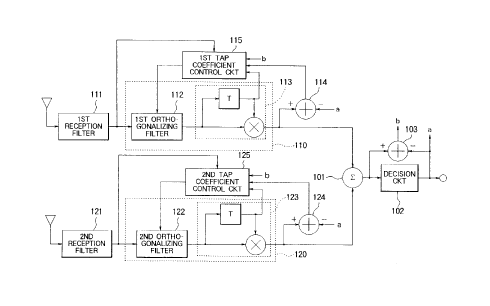
Referring to Fig. 5, a DS/CDMA receiver according
to a first embodiment of this invention is effective when
it is used in a narrow-band CDMA system in which a signal
power drop resulting from fading is large and when a
reception signal contains, as a main transmission path
21~~817
13
response component of a high power, only one desired wave
component having an earliest arrival time instant as
illustrated in Fig. 4(a).
In Fig. 5, the DS/CDMA receiver comprises first
and second adaptive interference cancellers 110 and 120
for removing or cancelling an interference from DS/CDMA
signals received in two antenna branches, respectively,
an all output combiner 101 for combining all of output
signals from the adaptive interference cancellers 110 and
120, and a first tap coefficient control circuit 115 and
a second tap coefficient control circuit 125 which serve
as two interference canceller control circuits for
controlling the adaptive interference cancellers 110 and
120 independently with respect to the antenna branches.
Herein, the adaptive interference canceller 110
comprises a first orthogonalizing filter 112 as an
adaptive filter for producing tap coefficients orthogonal
to spreading codes of all other stations to remove the
interference, and a first differential or delay detection
circuit 113 for compensating phase fluctuation with
reference to a signal from which the interference has
been removed with respect to all other stations.
Likewise, the adaptive interference canceller 120
comprises a second orthogonalizing filter 122 and a
second differential detection circuit 123 which are
operable in the manner similar to the first differential
detection circuit 113 and to the differential detection
circuits 503 illustrated in Fig. 2.
2l~~Rl~l
14
In the DS/CDMA receiver, a DS/CDMA signal
received through one antenna branch is filtered by a
first reception filter 111 at a predetermined frequency
band to be produced as a filtered signal which is
referred to as a received signal. The first reception
filter 111 is referred to as a first receiving unit which
receives the DS/CDMA signal as the received signal.
Then, the filtered signal is orthogonalized by the first
orthogonalizing filter 112 controlled by the first tap
coefficient control circuit 115 supplied with the
filtered signal and is transmitted to the first
differential detection circuit 113 as an orthogonalized
filtered signal. In the first differential detection
circuit 113, a phase synchronizing circuit (or a delay
element) T synchronizes a phase of the orthogonalized
filtered signal to produce a synchronized signal which is
delivered to the first tap coefficient control circuit
115 and a multiplier. The multiplier multiplies the
synchronized signal by a predetermined weight to produce
a weight-multiplied synchronized signal which is
delivered to a subtractor 114 and the all output combiner
101. On the other hand, another DS/CDMA signal received
through the other antenna branch is filtered by a second
reception filter 121 <~t a predetermined frequency band to
be produced as a filtered signal which is also referred
to as a received signal. The second reception filter 121
is referred to as a second receiving unit which receives
the DS/CDMA signal as the received signal. Then, the
~15581~
15
filtered signal is orthogonalized by the second
orthogonalizing filter 122 controlled by the second tap
coefficient control circuit 125 supplied with the
filtered signal and is transmitted to the second
differential detecting circuit 123 as an orthogonalized
filtered signal. In the second differential detection
circuit 123, a phase synchronizing circuit (or a delay
element) T synchronizes a phase of the orthogonalized
filtered signal to produce a synchronized signal which is
delivered to the second tap coefficient control circuit
125 and a multiplier. The multiplier multiplies the
synchronized signal by a predetermined weight to produce
a weight-multiplied synchronized signal which is
delivered to a subtractor 124 and the all output combiner
101.
Specifically, the tap coefficients of the first
orthogonalizing filter 112 are calculated by the first
tap coefficient control circuit 115. The tap
coefficients of the second orthogonalizing filter 122 are
calculated by the second tap coefficient control circuit
125. Each of the orthogonalizing filters 112 and 122 is
implemented by a linear adaptive filter as illustrated in
Fig. 3.
Supplied from the all output combiner 101 with a
synchronized combined signal representative of a total
sum of the weight-multiplied synchronized signals, a
decision circuit 102 produces a decision signal a
representative of a result of decision of whether the
z~~5s17
16
synchronized combined signal has a positive sign or a
negative sign. Those input and output signals to and
from the decision circuit 102 are supplied to a
subtractor 103. A subtraction signal b representative of
a subtraction result (input - output) is delivered to the
first tap coefficient control circuit 115 and the second
tap coefficient control circuit 125. The decision signal
a which is the output signal of the decision circuit 102
is delivered to the subtractors 114 and 124. Supplied
with the multiplied signal from the multiplier in the
first differential detection circuit 113 and with the
decision signal a from the decision circuit 102, the
subtractor 114 produces a subtraction signal (multiplied
signal - decision signal a) to be delivered to the first
tap coefficient control circuit 115. Supplied with the
multiplied signal from the multiplier in the second
differential detection circuit 123 and with the decision
signal a from the decj_sion circuit 102, the subtractor
124 produces a subtraction signal (multiplied signal -
decision signal a) to be delivered to the second tap
coefficient control cj_rcuit 125.
In the DS/CDMA receiver, the adaptive
interference cancellex-s 110 and 120 comprise a
combination of the ort.hogonalizing filter 112 and the
differential detection circuit 113 and a combination of
the orthogonalizing filter 122 and the differential
detection circuit 123, respectively. However, the
adaptive interference canceller may comprise an adaptive
2155817
17
filter for producing t.ap coefficients orthogonal to
spreading codes of all. other stations to remove an
interference. Alternatively, the adaptive interference
canceller may comprise an adaptive filter for producing
tap coefficients orthogonal to spreading codes of all
other stations to remove an interference, and
synchronization detecting circuit for compensating phase
fluctuation resulting from fading with reference to a
signal from which an interference from other stations has
been removed. In addition, use may be made of a
structure disclosed in Japanese Patent Application No. 5-
169092 (namely, 16909'./1993) and those structures
disclosed in the above-mentioned references 1 through 7.
The principle of orthogonalization is described in detail
in the above-mentioned Japanese Patent Application No. 5-
169092 and in the reference 7.
In this DS/CDMA receiver, it is expected that the
signal power drop resulting from fading is independent
between the antenna branches. This reduces a probability
of simultaneous power drop of the DS/CDMA signals in
these antenna branches. In the DS/CDMA receiver, each
antenna branch independently receives the DS/CDMA signal
subjected to an influence of fading. After the
interference from other stations is removed at each
antenna branch, diversity combination is carried out.
Thus, an excellent reception quality is maintained at a
low C/N value.
~~1~5~~.''l
18
As the subtraction signal b delivered to the tap
coefficient control circuit 115 and 125, use may be made
of an error signal in the DS/CDMA signal received through
each antenna branch or an error signal by a combined
signal which is a combination thereof. As a specific
control scheme in such. an event, use can be made of a
method described in th.e reference 7 for example.
Referring to Fig. 6, a DS/CDMA receiver according
to a second embodiment. of this invention is also
effective when it is used in a narrow-band CDMA system in
which a signal power drop resulting from fading is large.
In Fig. 6, the DS/CDMA receiver comprises two adaptive
interference cancellers for removing an interference in
correspondence to two antenna branches, respectively, an
all output combiner 201 for combining all of output
signals from the adaptive interference cancellers, and
tap coefficient control circuit 204 which serves as a
single interference canceller control circuit for
controlling the adaptive interference cancellers in
common with respect to the antenna branches.
The tap coefficient control circuit 204 carries
out common control by the use of best quality control
information relating to one of the antenna branches that
has a most excellent signal quality. One of the adaptive
interference cancellers comprises a first orthogonalizing
filter 212 as an adaptive filter for producing tap
coefficients orthogonal to spreading codes of all other
stations to remove the interference, and a first
zl~~s~7
19
differential detection circuit 213 for compensating phase
fluctuation with reference to a signal from which the
interference has been removed with respect to all other
stations. The other adaptive interference canceller
comprises a second orthogonalizing filter 222 and a
second differential detection circuit 223 which are
operable in a similar manner as mentioned above. Thus,
each adaptive interference canceller is separated into
the orthogonalizing filter and the differential detection
circuit. With this structure, an interference removing
function and a carrier wave phase compensating function
are separated.
With the adaptive interference canceller of the
above-mentioned structure, it is possible to stably
obtain the tap coefficients of the orthogonalizing
filters irrespective of the phase and the amplitude of a
user's station signal once the spreading codes of all
stations in the DS/CDMA system and the timings thereof
are determined, as des~~ribed in the reference 7.
Accordingly, in this DS/CDMA receiver, the same value can
be used as the tap coefficients of the orthogonalizing
filters 212 and 222. It is noted here that, if the same
value is used as the tap coefficients in the DS/CDMA
receiver of Fig. 5, control of the tap coefficients
inevitably becomes unstable when a C/I ratio (carrier
wave power/interference wave power) is decreased due to
fading with respect to each antenna branch. This is
because the tap coefficient control circuit 115 and 125
X155817
20
carry out tap control independently with respect to the
respective antenna branches.
In this DS/CDMA receiver, a DS/CDMA signal
received through one antenna branch is filtered by a
first reception filter 211 at a predetermined frequency
band to be produced a~: a filtered signal which is
referred to as a received signal. The first reception
filter 211 is referred to as a first receiving unit which
receives the DS/CDMA signal as the received signal.
Then, the filtered signal is orthogonalized by the first
orthogonalizing filter- 112 controlled by the tap
coefficient control cj.rcuit 204 supplied with the
filtered signal and is transmitted to the first
differential detection circuit 213 as an orthogonalized
filtered signal. In the first differential detection
circuit 213, a phase :synchronizing circuit T synchronizes
a phase of the orthogc>nalized filtered signal to produce
a synchronized signal which is delivered to the tap
coefficient control circuit 204 and a multiplier. The
multiplier multiplies the synchronized signal by a
predetermined weight t.o produce a weight-multiplied
synchronized signal which is delivered to a subtractor
214 and the all output. combiner 101.
On the other hand, another DS/CDMA signal
received through the other antenna branch is filtered by
a second reception filter 221 at a predetermined
frequency band to be produced as a filtered signal which
is referred to as a received signal. The second
215581
21
reception filter 221 is referred to as a second receiving
unit which receives the DS/CDMA signal as the received
signal. Then, the filtered signal is orthogonalized by
the second orthogonalizing filter 222 controlled by the
tap coefficient control circuit 204 supplied with the
filtered signal and is transmitted to the second
differential detection circuit 223 as an orthogonalized
filtered signal. In the second differential detection
circuit 223, a phase synchronizing circuit T synchronizes
a phase of the orthogonalized filtered signal to produce
a synchronized signal which is delivered to the tap
coefficient control circuit 225 and a multiplier. The
multiplier multiplies the synchronized signal by a
predetermined weight to produce a weight-multiplied
synchronized signal which is delivered to a subtractor
224 and the all output combiner 201.
Supplied from the all output combiner 201 with a
synchronized combined signal representative of a total
sum of the weight-multiplied synchronized signals, a
decision circuit 202 produces a decision signal a
representative of a result of decision of whether the
synchronized combined signal has a positive sign or a
negative sign. Those input and output signals to and
from the decision circuit 202 are supplied to a
subtractor 203. A subtraction signal b representative of
a subtraction result (input - output) is delivered to the
tap coefficient control circuit 204. The decision signal
a which is the output signal of the decision circuit 202
2L~a817
22
is delivered to the subtractors 214 and 224. Supplied
with the multiplied signal from the multiplier in the
first differential detection circuit 213 and with the
decision signal a from the decision circuit 202, the
subtractor 214 produces a subtraction signal (multiplied
signal - decision signal a) to be delivered to the tap
coefficient control circuit 204. Supplied with the
multiplied signal from the multiplier in the second
differential detection circuit 223 and with the decision
signal a from the decision circuit 202, the subtractor
224 produces a subtraction signal (multiplied signal -
decision signal a) to be delivered to the tap coefficient
control circuit 204.
In the above-described DS/CDMA receiver, the tap
coefficient control circuit 204 calculates the tap
coefficient which is used in common to the antenna
branches by the use of the best quality control
information. It is therefore possible to avoid
instability in controlling the tap coefficients. Like in
the DS/CDMA receiver of Fig. 5, an excellent reception
quality is maintained at a low C/N level.
Summarizing, the tap coefficient control circuit
204 serves as the single interference canceller control
circuit. The single interference canceller control
circuit controls first and second adaptive interference
cancellers (212 + 213 and 222 + 223) in common on the
basis of best quality control information relating to one
of the received signals of the first and the second
23
receiving units (211 and 221) that has a best signal
quality among the received signals of the first and the
second receiving units..
Referring to F'ig. 7, a DS/CDMA receiver according
to a third embodiment of this invention is effective when
it is used in a narrow-band CDMA system in which a signal
power drop resulting from fading is large and when a
plurality of transmission path response components are
present in a DS/CDMA signal received through each antenna
branch in a frequency selective fading environment in
which delay waves having late arrival time instants are
present in addition to a desired wave having an earliest
arrival time instant, as illustrated in Fig. 4(b).
In Fig. 7, they DS/CDMA receiver comprises a
plurality of adaptive interference cancellers for
removing an interference individually from a desired wave
having an earliest arrival time instant and a plurality
of delayed waves having late arrival time instants with
respect to two antenna branches, respectively, an all
output combiner 301 for combining all of output signals
from the adaptive interference cancellers, and 11-th
through ln-th tap coefficient control circuits 30411
through 3041n and 21-t.h through 2n-th tap coefficient
control circuits 30421 through 3042n as a plurality of
interference canceller control circuit for controlling a
plurality of the adaptive interference cancellers in one-
to-one correspondence to the desired wave and the delayed
waves independently with respect to the respective
215581
24
antenna branches.
The plurality of adaptive interference cancellers
comprise 11-th through ln-th orthogonalizing filters 3131
through 313n and 21-th through 2n-th orthogonalizing
filters 3231 through 323n as a plurality of adaptive
filters for producing tap coefficients orthogonal to
spreading codes of all other stations to remove the
interference, and 11-th through ln-th differential
detection circuit 3141 through 314n and 21-th through
2n-th differential detection circuit 3241 through 324n
for compensating phase fluctuation with reference to a
signal from which the interference has been removed with
respect to all other stations. Thus, the adaptive
interference cancellers are provided in one-to-one
correspondence to the desired wave and the delayed waves
with respect to each antenna branch.
In the DS/CDMA receiver, a DS/CDMA signal
received through one antenna branch is filtered by a
first reception filter 311 (which is referred to as a
first receiving unit) at a predetermined frequency band
to be produced as a filtered signal which is referred to
as a received signal. Thereafter, the filtered signal is
orthogonalized by the orthogonalizing filters 3131 to
313n controlled by the tap coefficient control circuits
3041n to 3041n supplied with a plurality of delayed
signals rll to rln obtained by delaying the filtered
signal at a plurality of phase synchronizing circuits (T1
to Tn_1) 3121 to 312n with a delay of (Ti + ... + Ti-1)
~1~581~
25
for an (i-1)-th (i = 2 to n) delayed wave. The signals
rin and rii are referred to as primary and secondary wave
components of the received signal, respectively. The
secondary wave component follows the primary wave
component in the received signal. Orthogonalized
filtered signals are transmitted to the differential
detection circuits 3141 to 314n. In the differential
detection circuits 3141 to 314n, phase synchronizing
circuits T synchronize phases of the orthogonalized
filtered signals to produce synchronized signals dii to
dln which are delivered to the tap coefficient control
circuit 30411 to 3041n and multipliers in the
differential detection circuits. The multipliers
multiply the synchroni;aed signals dii to din by
predetermined weights to produce weight-multiplied
signals which are delivered to a combiner 315. The
combiner 315 combines 'the signals into a combined signal
which is delivered to .a subtractor 316 and the all output
combiner 301.
A DS/CDMA signal received through the other
antenna branch is filtered by a second reception filter
321 (which is referred to as a second receiving unit) at
a predetermined frequency band to be produced as a
filtered signal which as also referred to as a received
signal. Thereafter, the filtered signal is
orthogonalized by the orthogonalizing filters 3231 to
323n controlled by the tap coefficient control circuits
30421 to 3042n supplied with a plurality of delayed
215581
26
signals r21 to r2n obtained by delaying the filtered
signal at a plurality of phase synchronizing circuits (T1
to Tn_1) 3221 to 322n with a delay of (Ti + ... + Ti-1)
for an (i-1)-th (i - 2 to n) delayed wave. The signals
r2n and r21 are also referred to as the primary and the
secondary wave components of the received signal,
respectively. Orthogonalized filtered signals are
transmitted to the differential detection circuits 3241
to 324n. In the differential detection circuits 3241 to
324n, phase synchronizing circuits T synchronize phases
of the orthogonalized :filtered signals to produce
synchronized signals d;21 to d2n which are delivered to
the tap coefficient control circuits 30421 to 3042n and
multipliers in the differential detection circuit. The
multipliers multiply the synchronized signals d21 to d2n
by predetermined weights to produce weight-multiplied
signals which are delivered to a combiner 325. The
combiner 325 combines 'the signals into a combined signal
which is delivered to a subtractor 326 and the all output
combiner 301. Thus, the tap coefficients of the
orthogonalizing filters 3131 to 313n are calculated by
the tap coefficient control circuits 30411 to 3041n while
the tap coefficients o:f the orthogonalizing filters 3231
to 323n are calculated by the tap coefficient control
circuits 30421 to 3042n.
Supplied from the all output combiner 301 with a
synchronized combined signal representative of a total
sum of the weight-multiplied synchronized signals, a
21W817
27
decision circuit 302 produces a decision signal a
representative of a result of decision of whether the
synchronized combined signal has a positive sign or a
negative sign. Those input and output signals to and
from the decision circuit 302 are supplied to a
subtractor 303. A subtraction signal b representative of
a subtraction result (input - output) is delivered to the
tap coefficient control circuits 30411 to 3041n and 30421
to 3042n. The decision signal a which is the output
signal of the decision circuit 302 is delivered to the
subtractors 316 and 326. Supplied with the combined
signal from the combiner 315 and with the decision signal
a, the subtractor 316 produces a subtraction signal
(combined signal - decision signal a) to be delivered to
the tap coefficient control circuits 30411 to 3041n'
Supplied with the combined signal from the combiner 325
and with the decision signal a, the subtractor 326
produces a subtraction signal (combined signal - decision
signal a) to be delivered to the tap coefficient control
circuits 30421 to 3042n'
In the DS/CDMA receiver, the desired wave and the
delayed waves are subjected to interference removal by
the orthogonalizing filters 3131 and 3141 (i - 1 through
n, i = 1 representing the desired wave, i = 2 through n
representing the delayed waves) and to phase
synchronization by the differential detection circuits
3141 and 3241 (i - 1 through n). The combiners 315 and
325 combine those outputs for the desired wave and the
2155817
28
delayed waves. In the orthogonalizing filters 3131 and
3141 (i = 1 through n) in the respective branches,
adaptive control of the tap coefficients are
independently carried out so that those components having
different arrival time instants are dealt with as
interferences to remove influences therefrom, not only
with respect to the other station's signals but also with
respect to the user's station signal.
Like the foregoing embodiments, this DS/CDMA
receiver can achieve an excellent reception quality at a
low C/N value. Particularly, the receiver according to
this embodiment presents both a spatial diversity effect
obtained by combining the DS/CDMA signals received
through the respective antenna branches and a path
diversity effect obtained by combining multipath wave
components.
Referring to Fag. 8, a DS/CDMA receiver according
to a fourth embodiment of this invention is effective
when it is used in a n<~rrow-band CDMA system in which a
signal power drop resu:Lting from fading is large and when
a plurality of transmission path response components are
present in a DS/CDMA signal received through each antenna
branch in a frequency selective fading environment in
which delayed waves are present in addition to the
desired wave, like the DS/CDMA receiver of Fig. 7.
In Fig. 8, the DS/CDMA receiver comprises a
plurality of adaptive interference cancellers for
removing an interference individually from a desired wave
2155817
29
and a plurality of delayed waves with respect to two
antenna branches, respectively, an all output combiner
401 for combining all ~of output signals from the adaptive
interference cancellers, and first through n-th tap
coefficient control circuits 4041 through 404n as a
plurality of interference canceller control circuits for
controlling the adaptive interference cancellers in one-
to-one correspondence to the desired wave and the delayed
waves in common with respect to the respective antenna
branches.
Herein, each of the tap coefficient control
circuits 4041 to 404n carries out common control by the
use of desired wave best quality control information
relating to one of the antenna branches that has a best
signal quality with respect to the desired wave and
delayed wave best quality control information relating to
one of the antenna branches that has a best signal
quality with respect t~o the delayed waves. The adaptive
interference cancellers comprise 11-th through ln-th
orthogonalizing filters 4131 to 413n and 21-th through
2n-th orthogonalizing filters 4231 to 423n as adaptive
filters for producing tap coefficients orthogonal to
spreading codes of all other stations to remove the
interference, and 11-th through ln-th differential
detection circuits 4141 to 414n and 21-th through 2n-th
differential detection circuits 4241 to 424n for
compensating phase fluctuation with reference to a signal
from which the interference has been removed with respect
21x5817
30
to all other stations. Thus, each adaptive interference
canceller is separated into the orthogonalizing filter
and the differential detection circuit. With this
structure, an interference removing function and a
carrier wave phase compensation function are separated.
With the adaptive interference canceller of the
above-mentioned structure, it is possible to stably
obtain the tap coefficients of the orthogonalizing
filters individually for the desired wave and the delayed
waves irrespective of the phase and the amplitude of
delayed wave components relating to the user's station
signal, once the spreading codes of all stations in the
DS/CDMA system and the timings thereof are determined.
Accordingly, in this DS/CDMA receiver, the same tap
coefficient value can be used in the orthogonalizing
filters for the same desired wave or the same delayed
wave. For example, the same tap coefficient value can be
used for the orthogonalizing filter 4131 corresponding to
the desired wave and for the orthogonalizing filter 4231
in the second branch corresponding to the same desired
wave. Likewise, another same tap coefficient value can
be used for the orthogonalizing filter 413n corresponding
to the n-th delayed wave and for the orthogonalizing
filter 423n corresponding to the same n-th delayed wave.
It is noted here that, if the same value is used as the
tap coefficients in the DS/CDMA receiver according to the
third embodiment of this invention, control of the tap
coefficients inevitably becomes unstable when a C/I ratio
21~~~1~
31
(carrier wave power/interference wave power) is decreased
due to fading with respect to each antenna branch. This
is because the tap control is carried out independently
with respect to the desired wave and the delayed waves.
In this DS/CDMA receiver, a DS/CDMA signal
received through one antenna branch is filtered by a
first reception filter 411 (which is referred to as a
first receiving unit) at a predetermined frequency band
to be produced as a filtered signal which is referred to
as a received signal. Thereafter, the filtered signal is
orthogonalized by the orthogonalizing filters 4131 to
413n controlled by the tap coefficient control circuits
4041 to 404n supplied with a plurality of delayed signals
rll to rln obtained by delaying the filtered signal at a
plurality of phase synchronizing circuits (T1 to Tn-1)
4121 to 412n with a delay of (Ti + ... + Ti-1) for an
(i-1)-th (i = 2 to n) delayed wave. The signals rln and
rll are referred to as the primary and the secondary wave
components of the received signal, respectively.
Orthogonalized filtered signals are transmitted to the
differential detection circuits 4141 to 414n. In the
differential detection circuits 4141 to 414n, phase
synchronizing circuits T synchronize phases of the
orthogonalized filtered signals to produce synchronized
signals dll to dln which are delivered to the tap
coefficient control circuits 40411 to 4041n and
multipliers in the differential detection circuits. The
multipliers multiply the synchronized signals dll to dln
~1~~817
32
by predetermined weights to produce weight-multiplied
signals which are delivered to a combiner 415. The
combiner 415 combines the signals into a combined signal
which is delivered to <~ subtractor 416 and the all output
combiner 401.
A DS/CDMA signal received through the other
antenna branch is filtered by a second reception filter
421 (which is referred to as a second receiving unit) at
a predetermined frequency band to be produced as a
filtered signal which .Ls also referred to as a received
signal. Thereafter, the filtered signal is
orthogonalized by the orthogonalizing filters 4231 to
423n controlled by the tap coefficient control circuits
4041 to 404n supplied with a plurality of delayed signals
r21 to r2n obtained by delaying the filtered signal at a
plurality of phase syn<:hronizing circuits (T1 to Tn_1)
4221 to 422n with a delay of (Ti + ... + Ti-1) for an
(i-1)-th (i = 2 to n) delayed wave. The signals r2n and
r21 are also referred i~o as the primary and the secondary
'wave components of the received signal, respectively.
~Drthogonalized filtered signals are transmitted to the
differential detection circuits 4241 to 424n. In the
differential detection circuits 4241 to 424n, phase
synchronizing circuits T synchronize phases of the
o rthogonalized filtered signals to produce synchronized
;signals d21 to d2n which are delivered to the tap
coefficient control circuits 4041 to 404n and multipliers
in the differential detection circuit. The multipliers
215581
33
multiply the synchronized signals d21 to d2n by
predetermined weights to produce weight-multiplied
signals which are delivered to a combiner 425. The
combiner 425 combines the signals into a combined signal
which is delivered to a subtractor 426 and the all output
combiner 401. Thus, the tap coefficients of the
orthogonalizing filters 4131 to 413n and the
orthogonalizing filters 4231 to 423n are calculated by
the tap coefficient control circuits 4041 to 404n.
Supplied from the all output combiner 401 with a
synchronized combined signal representative of a total
sum of the weight-multiplied synchronized signals, a
decision circuit 402 produces a decision signal a
representative of a result of decision of whether the
synchronized combined signal has a positive sign or a
negative sign. Those input and output signals to and
from the decision circuit 402 are supplied to a
subtractor 403. A subtraction signal b representative of
a subtraction result (input - output) is delivered to the
tap coefficient control circuits 4041 to 404n. The
decision signal a which is the output signal of the
decision circuit 402 is delivered to the subtractors 416
and 426. Supplied with the combined signal from the
combiner 415 and with the decision signal a, the
subtractor 416 produces a subtraction signal (combined
signal - decision signal a) to be delivered to the tap
coefficient control circuits 4041 to 404n. Supplied with
the combined signal from the combiner 425 and with the
2~~~81~
34
decision signal a, the subtractor 426 produces a
subtraction signal (combined signal - decision signal a)
to be delivered to the tap coefficient control circuits
4041 to 404n.
In the above-mentioned DS/CDMA receiver, the tap
coefficient control circuit 4041 (i = 1 to n) calculate
the tap coefficients used in common to the respective
antenna branches by the use of the best quality control
information. It is therefore possible to avoid
instability in controlling the tap coefficients. Thus,
an excellent reception quality can be maintained at a low
C/N value, like the foregoing embodiments.
Summarizing, the tap coefficient control circuit
404n serves as a single primary interference canceller
control circuit. The ;single primary interference
canceller control circuit controls first and second
primary adaptive interference cancellers (413n + 414n and
423n + 424n) in common on the basis of primary wave best
quality control information relating to one of the
primary wave components of the received signals of the
first and the second receiving units (411 and 421) that
has a best signal quality among the primary wave
components of the received signals of the first and the
second receiving units.
Likewise, the 'tap coefficient control circuit
4041 serves as a single secondary interference canceller
control circuit. The :single secondary interference
canceller control circuit controls first and second
21.~581'~
35
secondary adaptive interference cancellers (4131 + 4141
and 4231 + 4241) in common on the basis of secondary wave
best quality control j.nformation relating to one of the
secondary wave components of the received signals of the
first and the second receiving units (411 and 421) that
has a best signal quality among the secondary wave
components of the received signals of the first and the
second receiving units.
Among the above-mentioned embodiments, the
DS/CDMA receivers according to the third and the fourth
embodiments of this invention are described as the
structures adapted for use in a multiwave environment
with a number of delayed waves. In case where the
adaptive interference canceller itself has a path
diversity effect, the adaptive interference canceller can
be implemented, for example, by a single orthogonalizing
filter having a tap length over a plurality of symbols.
In such an event, the DS/CDMA receivers according to the
first and the second embodiments of this invention can be
adapted for use in a frequency selective fading
environment with delayed waves. In the foregoing
embodiments, each of the adaptive interference cancellers
comprises the adaptive filter for producing the tap
coefficients orthogonal to the spreading codes of all
other stations to remove the interference, and the
differential detection circuit for compensating phase
fluctuation with reference to the signal from which the
interference has been removed with respect to all other
~1~~81~
36
stations. However, the differential detection circuit
may be replaced by the synchronization detection circuit
having an equivalent phase fluctuation compensating
function. Although the number m of antenna branches is
two in the foregoing embodiments, a similar effect is
obtained when the number m of the antenna branches is
three or more.
As described, in the DS/CDMA receiver according
to this invention, it .Ls possible to maintain a desired
reception quality at a low C/N value even if it is used
in the narrow-band CDMA system in which the signal power
drop resulting from fading is large. In particular, this
DS/CDMA receiver is adapted for use in the frequency
selective fading environment in which the delayed waves
are present in addition to the desired wave, namely, in
case where a plurality of the transmission path response
components are present in the DS/CDMA signal received
through each antenna branch.