Note: Descriptions are shown in the official language in which they were submitted.
WO 95/23460 PCT/US95/02125
1
METHOD AND APPARATUS FOR CORRECTION AND LIMITATION OF TRANSMITTER POWER
ON THE REVERSE LINK OF A MOBILE RADIO TELEPHONE SYSTEM
' BACKGROUND OF THE INVENTION
I. Field of the Invention
The present invention relates to radio communications. More
particularly, the present invention relates to power control in a radio
telephone system.
II. Description of the Related Art
The Federal Communications Commission (FCC) governs the use of
the radio frequency (RF) spectrum. The FCC allocates certain bandwidths
within the RF spectrum for specific uses. A user of an allocated bandwidth
of the RF spectrum must take measures to ensure that the radiated
emissions inside and outside of that bandwidth are maintained within
acceptable levels to avoid interfering with other users operating in the same
and or other bandwidths. These levels are governed by both the FCC and the
particular user groups of said bandwidth.
The 800 MHz cellular telephone system operates its forward link, the
cell to radiotelephone transmission, in the bandwidth of 869.01 MHz to
893.97 MHz and the reverse link, the radiotelephone to cell transmission, in
the bandwidth of 824:01 MHz to 848.97 MHz. The forward and reverse link
bandwidths are split up into channels each of which occupies a 30 kHz
bandwidth. A particular user of the cellular system may operate on one or
several of these channels at a time. All users of the system must ensure that
they are compliant with the level of radiated emissions allowable inside and
outside of the channel or channels that they have been assigned.
There are several different techniques of modulation that can be used
in the cellular telephone system. Two examples of modulation techniques
are frequency division multiple access (FDMA) and code division multiple
access (CDMA).
The FDMA modulation technique generates signals that occupy one
channel at a time while the CDMA modulation technique generates signals
that occupy several channels. Both of these techniques must control their
return link radiated emissions to within acceptable limits inside and outside
of the assigned channel or channels. For maximum system performance,
WO 95/23460 PCT/US95/02125
2
users of the CDMA technique must carefully control the level of radiated
power inside the channels in which they are operating.
FIG. 1 shows a typical prior cellular radiotelephone. In both an FDMA
and a CDMA based radiotelelahone, there exists the possibility of driving the
power amplifier (101) in the transmitter beyond a point where acceptable out
of channel radiated emissions are maintained. This is primarily due to the
increased distortion output levels of the power amplifier (101) at high
output powers. Also, driving the power amplifier (101) beyond a certain
point can cause interference internal to the radio. For example, PA
puncturing in CDMA affects synthesizer phase noise due to large current
transitions. Both of these issues cause unacceptable radio performance.
Maintaining the proper on-channel output power can be difficult due
to several undesirable effects in the radiotelephone hardware. For example,
the CDMA based radio must implement a power control system that
operates over a very wide dynamic range, 80dB to 90dB, such that the
transmitted output power is linearly related to the received input power.
Closed loop and open loop power control together determine the
return link transmit energy, as disclosed in U.S. Patent No. 5,056,109 to
Gilhousen et al. and assigned to Qualcomm, Incorporated. Therefore, the
linear and nonlinear errors produced in both the receiver (103) and
transmitter (102) RF sections can cause unacceptable power control
performance. Also, both the FDMA and CDMA based radios must operate
on different channels while maintaining acceptable output power levels.
Variation in output power level and input power detection versus
frequency can cause an unacceptable amount of error in the amount of
return link transmitted energy.
These issues present significant problems to the designer of both
FDMA and CDMA based radiotelephones. There is a resulting need for an
effective, cost efficient means of correcting these problems.
SUMMARY OF THE INVENTION
The process of the present invention enables a radiotelephone to
operate in a linear fashion over a wide dynamic range while maintaining
acceptable transmit output power levels inside and outside of the return '
link bandwidth. The forward and return link power are measured by power
detectors and input to an analog to digital converter accessible by both
control hardware and/or software. The closed loop power control setting is
also monitored. The radiotelephone uses the detected power levels and
CA 02158577 1999-06-10
3
closed loop power control setting to index a set of correction
tables that indicate the reverse link transmit power error and
desired power amplifier biasing for the particular operating
point. The radiotelephone also determines if the transmitter
is operating above a maximum set point the transmit gain and
power amplifier biasing of the radiotelephone are adjusted to
correct the undesired error and maintain the desired output
power.
In accordance with the present invention there is
provided a method for correcting transmit power of a radio
device having a plurality of predetermined calibration values
and a reference voltage signal, the radio device transmitting
and receiving on a plurality of frequencies, each frequency
having a frequency index, the method comprising the steps of:
receiving a first signal having a first gain, a first
frequency of the plurality of frequencies, and the first
frequency having a first frequency index; determining a
receive power value of the first signal; generating an
automatic gain control setpoint in response to the receive
power value and the reference voltage signal; selecting a
first predetermined calibration value in response to the
automatic gain control setpoint and the first frequency index;
adjusting the first gain in response to the first calibration
value; transmitting a second signal having a second gain and a
second frequency of the plurality of frequencies, the second
frequency having a second frequency index; determining a
transmit power value of the second signal; generating a second
calibration value in response to the automatic gain control
CA 02158577 1999-06-10
3a
setpoint, the second frequency index, and the transmit power
value; and adjusting the second gain in response to the second
calibration value.
BRIEF DESCRIPTION OF THE DRAWINGS
Fig. 1 shows a block diagram of a typical prior art
radiotelephone frequency section for use in a radiotelephone
system.
Fig. 2 shows a block diagram of the preferred embodiment
power control correction implementation.
Fig. 3 shows a block diagram of the power limiting
control section as related to Fig. 2.
Fig. 4 shows a block diagram of the closed loop power
control section as related to Fig. 2.
Fig. 5 shows a block diagram of the PA limit threshold
control section as related to Fig. 2.
Fig. 6 shows an alternate embodiment of the present
invention that employs a power limiting control system based
on accumulator feedback control.
Fig. 7 shows an alternate embodiment of the present
invention that employs a power limiting control system based
on the closed loop power control accumulator.
Fig. 8 shows an alternate embodiment of the present
invention that employs a power limiting control system based
on integral feedback control.
Fig. 9 shows an alternate embodiment of the present
invention that employs a power limiting control system based
CA 02158577 1999-06-10
3b
on a measure of receive power and the closed loop power
control setting to estimate output power.
DETAILED DESCRIPTION OF THE PREFERRED EMBODIMENTS
The process of the present invention provides power
control correction for a mobile radiotelephone as well as
maintaining acceptable in and out of band maximum emission
levels. This is accomplished by real-time
WO 95/23460 ~ PCTIUS95/02125
4
compensation utilizing a set of correction tables that are generated during
the production testing of each radiotelephone.
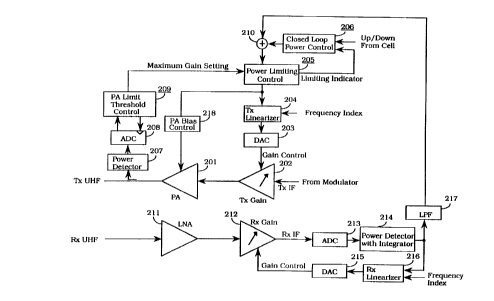
FIG. 2 shows a block diagram of a CDMA radiotelephone with the
preferred embodiment power control correction implementation. FIGs. 3, 4,
and 5 detail specific blocks of FIG. 2. The radiotelephone is comprised of a
receive linearization section, transmit linearization section, power amplifier
bias control section, and power limiting control section.
The receive linearization section includes an automatic gain control
(AGC) section. The signal input to the AGC section is received on the
forward link and amplified by a low noise amplifier (LNA) (211). The output
of the LNA (211) is input to a variable gain amplifier (212). The variable
gain
amplifier (212) produces a signal that is converted to a digital signal using
an
analog to digital converter (ADC) (213).
The power of the digitized received signal is next computed by a
digital power detector (214). The power detector (214) includes an integrator
that integrates the detected power with respect to a reference voltage. In the
preferred embodiment, this reference voltage is provided by the radio's
demodulator to indicate the nominal value at which the demodulator
requires the loop to lock in order to hold the power level constant. The
demodulator requires this value for optimum performance since a power
level too far out of the optimum range will degrade the performance of the
demodulator. The power detector (214) performs the integration, thus
generating an AGC setpoint. The setpoint and a receive frequency index are
input to a receiver linearizing table (216).
The AGC setpoint and the frequency index are used to address the
linearizer (216), thus accessing the proper calibration value. This
calibration
value is then output to a digital to analog converter (215) that generates the
analog representation of the receive AGC setting.
The analog value adjusts the biasing of the variable gain amplifier
(212). The control of the variable gain amplifier (212) forces the receive AGC
loop to close such that the input to the receiver linearizing table (216)
follows a predetermined straight line with respect to RF input power. This
linearization removes the undesired linear and non-linear errors in
addition to variations versus frequency that would otherwise be apparent at
the input to the receiver .linearizing table (216) in the receiver. These
errors
and variations would contribute to errors in the transmitter.
In order to reduce the error in the receive and transmit chains versus
frequency, the receive and transmit linearizers utilize the frequency index
that specifies the current center frequency on which the receive and
~WO 95/23460 I ~ PCTlUS95/02125
transmit chains are operating. During factory calibration of the
radiotelephone, the linearizers are loaded with values, in addition to the
previously mentioned calibration values, that are indexed by frequency to
correct the errors related to operating center frequency.
5 The AGC setpoint is the open loop power control signal for the radio.
In the preferred embodiment, this is the power control performed by the
radio by itself without control input from the cells. As the power of the
signal received from the cell increases, the radio decreases its transmit
power. This output power control is accomplished by the AGC setpoint that
is filtered by a low pass filter (217).
The transmit section includes a digital summer (210) that combines
the AGC setpoint and a closed loop power control setting (206). The output
of the summer (210) is fed into a power control limiting section (205). The
operation of the power control limiting section (205) and the closed loop
power control section (206), illustrated in FIGs. 3 and 4 respectively, will
be
discussed subsequently in greater detail.
The output of the power control limiting section (205), along with the
transmit frequency index, are used to address values stored in a transmitter
linearizing table (204). The transmitter linearizing table (204) contains
values determined from production testing of the radiotelephone. The
. selected value is input to a digital to analog converter (203) whose output,
an analog representation of the digital value input, controls a variable gain
amplifier (202).
The biasing of the variable gain amplifier (202) is adjusted by the
analog calibration value to a point such that the input to the transmitter
linearizing table (204) follows a predetermined straight line with respect to
transmitted RF output power. This linearization removes the undesired
linear and non-linear errors along with variations versus frequency in the
transmitter. This, combined with the previously mentioned receive
linearization, greatly reduces the open and closed loop power control errors
due to RF performance imperfections.
The power amplifier (PA) bias control section (218) controls the bias
point of the transmit PA (201) based on the transmit gain setting such that
the transmit sidebands for the given gain setting are optimized versus PA
(201) current consumption. This allows a battery powered telephone to
maximize talk time by reducing PA (201) current consumption at lower
output powers while still maintaining acceptable sideband levels at higher
output power levels.
WO 95/23460 PCT/US95/02125
- .. 6
The power control limiting section (205) is illustrated in FIG. 3. The
power control limiting section (205) controls the closed loop power control
and transmit gain settings when the output of the transmit gain summer
(210) corresponds to a transmit output power level which is equal to or .
greater than the intended maximum output power. The maximum gain
setting is determined by the PA limit threshold control section (209).
The threshold control section (209) determines the maximum gain
setting based on a nominal value that is modified by a real-time
measurement of the transmitted output power. The measurement is
accomplished by an analog power detector (207) whose output transformed
into a digital signal by an analog to digital converter (208). The digitized
power value is then input to the threshold control section (209).
The threshold control section, detailed in FIG. 5, operates by the high
power detector (HDET) linearizer (501) scaling the input digitized power
value in order to match the numerology of the digital transmit gain control
section. The scaled output from the linearizer (501) is subtracted (502) from
the nominal maximum gain setting. This maximum gain setting can be
hard coded into the radio during assembly or input during manufacturing
and testing of the radio.
The difference of the maximum gain setting and the scaled output
power is then added, by the adder (503), to the maximum gain setting. The
sum of these signals is then used as the corrected maximum gain setting.
This real-time modification of the detected power helps mitigate the errors
introduced by temperature variations and aging of the transmitter PAs. In
other words, if the difference between the maximum gain setting and the
real-time measured power value is 0, then no correction is necessary. If
there is a difference between the two, the difference is used to correct the
maximum gain setting.
Referring to FIG. 3, a digital comparator (301) detects when the output
of the transmit gain summer (210) equals or exceeds the maximum gain
setting. The comparator (301) controls a 2:1 multiplexes (302) that outputs
the maximum allowable setting when the output of the summer (210) .
exceeds the maximum allowable setting. When the output of the summer
(210) is less than the maximum allowable setting, the multiplexes (302)
outputs the direct output of the summer (210). This prohibits the
transmitter from exceeding its maximum operating point.
The closed loop power control section (206), illustrated in FIG. 4,
accumulates the power control commands sent on the forward link by the
controlling radiotelephone cell site and outputs a gain adjust signal. The
WO 95/23460 PCTIUS95/02125
7
power control commands are collected in an accumulator (401). The op-
eration of the accumulator (401) is controlled by the power control limiting
section (205) when the transmit power amplifier (201) is outputting the
maximum allowable power.
When the output of the summer (210) changes from being less than
. to equal or greater than the maximum allowable setting, the output of the
closed loop power control accumulator (401) is latched into a flip-flop (402).
While the output of the summer (210) is equal to or greater than the
maximum allowable setting, as determined by the comparator (403) and
NAND gate (404) circuit, an AND gate (405) masks off any closed loop power
control up commands that would force the accumulator (401) above the flip-
flop's (402) latched value. This prevents the accumulator from saturating
during power limiting yet allows the closed loop power control setting to
change anywhere below the latched value.
An alternate embodiment of the process of the present invention is
illustrated in FIG. 6. In this embodiment, a power limiting control system is
employed based on accumulator feedback control. The system operates by
first measuring the output power of the power amplifier (609) using a power
detector (610). The detected power is then digitized by an ADC (611) and
compared to a maximum allowable setting by the comparator (601). If the
output power is greater than the maximum setting, the power limiting
accumulator (602) begins turning power down by reducing the gain of the
variable gain amplifier (608). If the output power is less than the maximum
setting the power limiting accumulator (602) returns to a OdB correction
value.
In this embodiment, a closed loop power control limiting function
(604 and 605), similar to the preferred embodiment, is employed. However,
the trigger for the closed loop power control limiting function is a
comparator (603) that detects when the power limiting accumulator (602) is
limiting the output power by comparing the accumulator (602) output to
OdB with the comparator (603). The linearizing compensation tables, similar
to the tables in the preferred embodiment, are added into the transmit gain
control using a summer (606).
In another alternate embodiment, illustrated in FIG. 7, a power
limiting control system is employed that is based on the closed loop power
control accumulator (702). The system operates by first measuring the
output power of the power amplifier (705) using a power detector (706). The
detected power is digitized (707) and compared to a maximum allowable
setting by the comparator (701). If the output power is greater than the
WO 95/23460 ~' ~ ~ ~ ~ ~ PCT/US95/02125
8
maximum setting, the closed loop power control accumulator (702) is
modified to turn the amplifier (704) power down by one step each 1.25 ms
until the output power is less than the maximum setting. If the output
power is less than the maximum setting, the closed loop power control
accumulator is not modified. The linearizing compensation tables, similar
to the preferred embodiment, are added into the transmit gain control using
a summer (703).
In yet another embodiment, illustrated in FIG. 8, a power limiting
control system is employed that is based on integral feedback control. The
system operates by first measuring the output power of the power amplifier
(808) using a power detector (809). The detected power is digitized (810) and
input to an integrator (801) that follows the equation:
1
K ~ ~ (Setpoint - Detected)dt.
The integrator (801), generating a gain control signal, saturates at OdB
and -63dB of correction. The gain control signal is thus limited within a
range. If the output power is greater than the setpoint, the integrator turns
down the output power of the amplifier (807) at a rate based on the
integration constant K until the setpoint is reached. The integrator is
allowed to turn power down by as much as 63dB. If the output power is less
than the setpoint, the output of the integrator (801) will be forced to zero,
thus not adjusting output power.
In this embodiment, a closed loop power control limiting function
(803 and 804), similar to the preferred embodiment, is employed. The trigger
for the closed loop power control limiting function, however, is a
comparator (802) that detects when the power limiting integrator (801) is
limiting the output power. The linearizing compensation tables, similar to
the preferred embodiment, are added into the transmit gain control using a
summer (805).
In still another embodiment, illustrated in FIG. 9, a power limiting
control system is employed that is based only on a measure of receive '
power, as determined by the Rx power lookup table (902), and the closed
loop power control setting as opposed to actual output power. The transmit
power limiting and closed loop power control limiting function (901) can be
implemented with either the preferred embodiment using the saturating
accumulator (903) or one of the alternate embodiments. However, only the
W0 95/23460 ~~~" PCT/US95102125
9
receive power and closed loop power control setting are used to estimate
transmit output power.
In summary, the process of the present invention ensures that the
transmitted sidebands and synthesizer phase noise of a radio transmitter
remains within a predetermined specification by limiting the maximum
. output power. This power limitation is accomplished by a control loop
including a calibration look-up table. Therefore, a radiotelephone using the
process of the present invention would not exceed it's nominal maximum
power level due to the cell issuing too many power turn-up commands. The
radiotelephone limits the power output even when the cell erroneously
decides the radiotelephone power should be increased.
WE CLAIM: